EP1635465A2 - Sensor and method of operation of the same including noise compensation - Google Patents
Sensor and method of operation of the same including noise compensation Download PDFInfo
- Publication number
- EP1635465A2 EP1635465A2 EP05019008A EP05019008A EP1635465A2 EP 1635465 A2 EP1635465 A2 EP 1635465A2 EP 05019008 A EP05019008 A EP 05019008A EP 05019008 A EP05019008 A EP 05019008A EP 1635465 A2 EP1635465 A2 EP 1635465A2
- Authority
- EP
- European Patent Office
- Prior art keywords
- oscillator
- sense element
- signal
- filter
- gain control
- Prior art date
- Legal status (The legal status is an assumption and is not a legal conclusion. Google has not performed a legal analysis and makes no representation as to the accuracy of the status listed.)
- Withdrawn
Links
- 238000000034 method Methods 0.000 title claims abstract description 23
- 230000005291 magnetic effect Effects 0.000 claims abstract description 33
- 230000008859 change Effects 0.000 claims description 13
- 238000003466 welding Methods 0.000 claims description 7
- 230000004044 response Effects 0.000 claims description 6
- 239000003302 ferromagnetic material Substances 0.000 claims description 3
- ORQBXQOJMQIAOY-UHFFFAOYSA-N nobelium Chemical compound [No] ORQBXQOJMQIAOY-UHFFFAOYSA-N 0.000 description 23
- 238000010586 diagram Methods 0.000 description 18
- 239000011162 core material Substances 0.000 description 9
- 238000004519 manufacturing process Methods 0.000 description 5
- 230000007423 decrease Effects 0.000 description 4
- 229910052751 metal Inorganic materials 0.000 description 4
- 239000002184 metal Substances 0.000 description 4
- 230000000737 periodic effect Effects 0.000 description 4
- 239000003990 capacitor Substances 0.000 description 3
- 239000000463 material Substances 0.000 description 3
- 230000008569 process Effects 0.000 description 3
- 230000008878 coupling Effects 0.000 description 2
- 238000010168 coupling process Methods 0.000 description 2
- 238000005859 coupling reaction Methods 0.000 description 2
- 239000004065 semiconductor Substances 0.000 description 2
- 239000000758 substrate Substances 0.000 description 2
- 229910000859 α-Fe Inorganic materials 0.000 description 2
- JBRZTFJDHDCESZ-UHFFFAOYSA-N AsGa Chemical compound [As]#[Ga] JBRZTFJDHDCESZ-UHFFFAOYSA-N 0.000 description 1
- RYGMFSIKBFXOCR-UHFFFAOYSA-N Copper Chemical compound [Cu] RYGMFSIKBFXOCR-UHFFFAOYSA-N 0.000 description 1
- 229910001218 Gallium arsenide Inorganic materials 0.000 description 1
- XUIMIQQOPSSXEZ-UHFFFAOYSA-N Silicon Chemical compound [Si] XUIMIQQOPSSXEZ-UHFFFAOYSA-N 0.000 description 1
- 239000004020 conductor Substances 0.000 description 1
- 229910052802 copper Inorganic materials 0.000 description 1
- 239000010949 copper Substances 0.000 description 1
- 238000001514 detection method Methods 0.000 description 1
- 229910052732 germanium Inorganic materials 0.000 description 1
- GNPVGFCGXDBREM-UHFFFAOYSA-N germanium atom Chemical compound [Ge] GNPVGFCGXDBREM-UHFFFAOYSA-N 0.000 description 1
- 230000005426 magnetic field effect Effects 0.000 description 1
- 230000007257 malfunction Effects 0.000 description 1
- 230000035699 permeability Effects 0.000 description 1
- 229910021420 polycrystalline silicon Inorganic materials 0.000 description 1
- 229920005591 polysilicon Polymers 0.000 description 1
- 229920006395 saturated elastomer Polymers 0.000 description 1
- 229910052710 silicon Inorganic materials 0.000 description 1
- 239000010703 silicon Substances 0.000 description 1
- 230000001960 triggered effect Effects 0.000 description 1
Images



Classifications
-
- H—ELECTRICITY
- H03—ELECTRONIC CIRCUITRY
- H03K—PULSE TECHNIQUE
- H03K17/00—Electronic switching or gating, i.e. not by contact-making and –breaking
- H03K17/94—Electronic switching or gating, i.e. not by contact-making and –breaking characterised by the way in which the control signals are generated
- H03K17/945—Proximity switches
- H03K17/95—Proximity switches using a magnetic detector
- H03K17/952—Proximity switches using a magnetic detector using inductive coils
- H03K17/9537—Proximity switches using a magnetic detector using inductive coils in a resonant circuit
- H03K17/9542—Proximity switches using a magnetic detector using inductive coils in a resonant circuit forming part of an oscillator
-
- H—ELECTRICITY
- H03—ELECTRONIC CIRCUITRY
- H03K—PULSE TECHNIQUE
- H03K17/00—Electronic switching or gating, i.e. not by contact-making and –breaking
- H03K17/94—Electronic switching or gating, i.e. not by contact-making and –breaking characterised by the way in which the control signals are generated
- H03K17/945—Proximity switches
- H03K17/95—Proximity switches using a magnetic detector
- H03K17/9502—Measures for increasing reliability
-
- H—ELECTRICITY
- H03—ELECTRONIC CIRCUITRY
- H03K—PULSE TECHNIQUE
- H03K17/00—Electronic switching or gating, i.e. not by contact-making and –breaking
- H03K17/94—Electronic switching or gating, i.e. not by contact-making and –breaking characterised by the way in which the control signals are generated
- H03K17/945—Proximity switches
- H03K17/95—Proximity switches using a magnetic detector
- H03K17/952—Proximity switches using a magnetic detector using inductive coils
- H03K17/9537—Proximity switches using a magnetic detector using inductive coils in a resonant circuit
- H03K17/954—Proximity switches using a magnetic detector using inductive coils in a resonant circuit controlled by an oscillatory signal
Definitions
- Sensors for use in detecting targets and more particularly, sensors for use in detecting targets in the presence of an alternating current magnetic field.
- Sensors such as proximity sensors are used in industrial machinery, such as welding equipment and industrial robots.
- Proximity sensors detect the presence of material objects, such as metal targets.
- Proximity sensors are used to detect the presence of both stationary and non-stationary targets.
- a table for holding a work piece to be welded, such as an engine block is an example of a stationary target.
- To detect a table a proximity sensor is moved toward the table until the table is detected.
- a moving robotic arm such as a robotic arm moving a work piece, such as an engine block, onto a table is an example of a non-stationary target.
- a moving robotic arm is detected as it moves to a position near a proximity sensor.
- proximity sensors are used in environments that include arc welders. Arc welders create a electromagnetically noisy environment. Some sensors fail when used in such an electromagnetically noisy environment. A failed sensor can cause manufacturing lines to shut down or industrial machinery to malfunction. For these and other reasons there is a need for sensors that do not fail in the presence of a magnetic field.
- An apparatus including a sense element and an oscillator coupled to the sense element.
- the oscillator generates an oscillator signal and a gain control signal.
- the oscillator amplitude compensates the oscillator signal when noise is detected in the sense element.
- the noise has a frequency of about sixty hertz.
- the oscillator comprises a filter coupled to a transconductance amplifier.
- the filter receives the oscillator signal at a filter input port and provides the gain control signal at a filter output port.
- the filter comprises a highpass filter.
- the highpass filter has a cutoff frequency and the oscillator signal has a frequency below the cutoff frequency.
- the transconductance amplifier includes a gain port
- the filter includes a filter output port
- the filter output port is coupled to the gain input port.
- the sense element includes a coil including a magnetic core.
- the magnetic core comprises a ferromagnetic material.
- a method includes detecting a frequency shift in an oscillator signal and compensating for an amplitude change in the oscillator signal in response to the frequency shift.
- detecting a frequency shift in the oscillator signal includes processing the oscillator signal with a highpass filter.
- compensating for the amplitude change in the oscillator signal in response to the frequency shift includes adjusting a gain control signal provided to a transconductance amplifier.
- Another method includes detecting magnetic interference in a sense element coupled to an oscillator and adjusting a gain control signal in the oscillator to compensate for the magnetic interference.
- detecting magnetic interference in the sense element coupled to an oscillator includes detecting a frequency shift in an oscillator signal.
- adjusting the gain control signal in the oscillator to compensate for the magnetic interference includes passing an oscillator signal through a filter to adjust the gain control signal.
- a system includes a sense element, an oscillator coupled to the sense element, and a target to be detected by the sense element.
- the oscillator generates an oscillator signal and a gain control signal and the oscillator amplitude compensates the oscillator signal when noise is detected in the sense element and a target is detected by the sense element.
- the target comprises a moveable structure to be detected by the sense element.
- the moveable structure includes a welding unit.
- the target comprises a stationary structure to be detected by the sense element.
- the stationary structure comprises an arc welding unit.
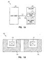
- Figure 1A illustrates a block diagram of an apparatus 100 including a sense element 102 and an oscillator 104 coupled to the sense element 102 in accordance with one embodiment.
- the sense element 102 has a sense element port 106.
- the oscillator 104 has an oscillator port 108.
- the sense element port 106 is coupled to the oscillator port 108.
- the coupling provides a channel 110 for sending signals, such as electronic signals, between the sense element 102 and the oscillator 104.
- the oscillator 104 includes an oscillator signal 112 and a gain control signal 114.
- Figure 1B illustrates the sense element 102, shown in Figure 1A, including a coil 116 and a magnetic core 118 in accordance with one embodiment.
- a conductive material such as a metal or polysilicon, is suitable for use in the fabrication of the coil 116. Copper is an exemplary metal suitable for use in the fabrication of the coil 116.
- the coil 116 is a discrete coil.
- the coil 116 is an integrated circuit coil and fabricated on a die.
- An integrated circuit coil is a coil fabricated with the same processes, such as the processes used to form the integrated circuits coupled to the coil, and on the same die as the integrated circuits coupled to the coil.
- a die is a substrate, such as a semiconductor substrate.
- Exemplary semiconductor materials suitable for use in forming a die in connection with the fabrication of the coil 116 include silicon, germanium, and gallium arsenide.
- Ferrite a ferromagnetic material, is an exemplary material suitable for use in connection with the fabrication of the magnetic core 118. Ferrite is suitable for use as a core material for a discrete coil or for an integrated circuit coil.
- the oscillator 104 generates the oscillator signal 112.
- the oscillator signal 112 is a substantially periodic signal.
- the sense element 102 senses the presence of a target.
- a metal plate is an exemplary target suitable for use in connection with the apparatus 100.
- an electrical property, such as the resistive loss, of the sense element 102 changes.
- a change in an electrical property of the sense element 102 produces a change in the oscillator signal 112.
- Detection of a change in the oscillator signal 112 indicates the presence of the target.
- the oscillator 104 generates the gain control signal 114.
- the gain control signal 114 is not limited to being a substantially periodic signal.
- the gain control signal 114 amplitude compensates the oscillator signal 112 when noise, such as magnetic noise produced by an arc welder, is present at the sense element 102.
- FIG 2 illustrates a block diagram of an apparatus 200 including the sense element 102, the oscillator 104, the oscillator signal 112, and the gain control signal 114, all shown in Figure 1A, and a filter 202 to receive the oscillator signal 112 and to provide the gain control signal 114 to a transconductance amplifier 204 in accordance with one embodiment.
- the sense element 102 has a sense element port 106.
- the oscillator 104 has an oscillator port 108.
- the sense element port 106 of the sense element 102 is coupled to the oscillator port 108 of the oscillator 104.
- the coupling provides a channel 110 for sending signals, such as electronic signals, between the sense element 102 and the oscillator 104.
- the oscillator 104 includes the filter 202 coupled to the transconductance amplifier 204.
- the filter includes a filter input port 206 and a filter output port 208.
- the filter 202 receives the oscillator signal 112 at the filter input port 206 and provides the gain control signal 114 at the filter output port 208.
- the filter 202 includes a highpass filter.
- a highpass filter is a filter which attenuates frequencies below its cutoff frequency. For the filter 202 having a highpass transfer function and a cutoff frequency, the oscillator signal 112 has a frequency below the cutoff frequency.
- the transconductance amplifier 204 converts a voltage to a current.
- the transconductance amplifier 204 includes an amplifier output port 210.
- the amplifier output port is coupled to the oscillator port 108.
- the transconductance amplifier 204 includes a gain control input port 214.
- the filter output port 208 is coupled to the gain control input port 214.
- the oscillator 104 In operation, the oscillator 104 generates the oscillator signal 112 and the gain control signal 114.
- the oscillator signal 112 is a substantially periodic signal. In some embodiments, the oscillator signal 112 is processed to form the gain control signal 114.
- the oscillator 104 amplitude compensates the oscillator signal 112 when noise is detected in the sense element 102. Amplitude compensation provided by the oscillator 104 adjusts the amplitude of the oscillator signal 112. For example, if the amplitude of the oscillator signal 112 decreases, then amplitude compensation increases (boosts) the amplitude of the oscillator signal 112.
- amplitude compensation decreases (suppresses) the amplitude of the oscillator signal 112.
- amplitude compensation is triggered when noise is present at the sense element 102.
- the noise that triggers amplitude compensation has a frequency of about sixty hertz.
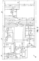
- Figure 3 illustrates a schematic diagram of an apparatus 300 including the sense element 102, shown in Figure 2, the oscillator 104, shown in Figure 2, and a bias circuit 302, an interface circuit 304, and an apparatus output port 306 in accordance with one embodiment.
- the channel 110 couples the sense element port 106 of the sense element 102 to the oscillator port 108 of the oscillator 104.
- the bias circuit 302 provides a bias current to the transconductance amplifier 204, shown in Figure 2.
- the bias circuit 302 is not limited to a particular topology.
- the bias circuit 302 includes an adjustable impedance 308.
- the bias circuit 302 is coupled to the interface circuit 304.
- the bias circuit 302 is coupled to a Schmitt trigger 310 included in the interface circuit 304.
- a Schmitt trigger includes a comparator that switches an output signal when an input signal passes in one direction through a reference voltage.
- the interface circuit 304 receives and processes the oscillator signal 112, shown in Figure 2, to provide a target detected signal at the apparatus output port 306.
- interface circuit 304 includes the Schmitt trigger circuit 310.
- the target detected signal is a current signal.
- Figure 4 illustrates a flow diagram of a method 400 for compensating for noise in an oscillator signal in accordance with one embodiment.
- the method 400 includes detecting a frequency shift in an oscillator signal (block 402), and compensating for an amplitude change in the oscillator signal in response to the frequency shift (block 404).
- detecting the frequency shift in the oscillator signal includes processing the oscillator signal with a highpass filter.
- compensating for the amplitude change in the oscillator signal in response to the frequency shift comprises adjusting a gain control signal provided to a transconductance amplifier.
- Figure 5 illustrates a flow diagram of a method 500 for compensating for magnetic interference in an oscillator signal in accordance with one embodiment.
- the method 500 includes detecting magnetic interference in a sense element coupled to an oscillator (block 502), and adjusting a gain control signal in the oscillator to compensate for the magnetic interference (block 504).
- detecting magnetic interference in the sense element coupled to the oscillator includes detecting a frequency shift in an oscillator signal.
- adjusting the gain control signal in the oscillator to compensate for the magnetic interference comprises passing an oscillator signal through a filter to adjust the gain control signal.
- Figure 6 illustrates a block diagram of a system 600 including the sense element 102 and the oscillator 104, shown in Figure 1A, and a target 602 in accordance with one embodiment.
- the sense element 102 includes the sense element port 106.
- the oscillator 104 includes the oscillator port 108.
- the channel 110 couples the sense element port 106 to the oscillator port 108.
- the target 602 is not limited to a particular target.
- the target 602 includes a moveable structure to be detected by the sense element 102.
- the moveable structure includes a welding unit.
- the target 602 includes a stationary structure to be detected by the sense element 102.
- Exemplary stationary structures includes tables and automobile bodies on an assembly line.
- the stationary structure includes an arc welding unit.
- the oscillator 104 In operation, the oscillator 104 generates the oscillator signal 112 and the gain control signal 114.
- the target 602 is detected by the sense element 102.
- the oscillator amplitude compensates the oscillator signal 112 when magnetic noise is detected in the sense element 102.
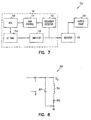
- FIG 7 illustrates a block diagram of an apparatus 700 including the apparatus 100, shown in Figure 1A, a rectifier 702 and an output stage 704 in accordance with one embodiment.
- the apparatus 100 includes the LC Tank 706, an operational transconductance amplifier 708, a gain control 710, a frequency detector 720, and an amplifier 730.
- the LC Tank 706 is coupled to the operational transconductance amplifier 708 and the amplifier 730.
- the operational transconductance amplifier 708 is coupled to the gain control 710.
- the LC Tank 706 is coupled to the amplifier 730.
- the frequency detector 720 is coupled to the gain control 710, the amplifier 730 and the rectifier 702.
- the rectifier 702 is coupled to the output stage 704.
- the operation transconductance amplifier 708 functions as a variable gain voltage controlled current source to drive the LC Tank 706.
- the oscillating frequency of the apparatus 100 increases.
- the change in the oscillating frequency is detected and converted into a gain change in the apparatus 100 to compensate the tank impedance change of the LC Tank 706 caused by the magnetic field.
- FIG 8 illustrates a schematic diagram of the LC Tank 706, shown in Figure 7, in accordance with one embodiment.
- the LC Tank 706 includes a resistor 802, an inductor 804, and a capacitor 806.
- the resistor 802 is in series with the inductor 804.
- the capacitor 806 is in parallel with the series combination of the resistor 802 and the inductor 804.
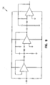
- FIG 9 illustrates a schematic diagram of the frequency detector 720, shown in Figure 7, in accordance with one embodiment.
- the frequency detector 720 includes a highpass filer having active elements configured with passive resistors and capacitors.
- the invention discloses an apparatus including a sense element and an oscillator.
- the oscillator is coupled to the sense element and is used to generate an oscillator signal and a gain control signal.
- the oscillator signal is amplitude compensated when noise is detected in the sense element.
- a method includes detecting magnetic interference in a sense element coupled to an oscillator, and adjusting a gain control signal in the oscillator to compensate for the magnetic interference.
Landscapes
- Inductance-Capacitance Distribution Constants And Capacitance-Resistance Oscillators (AREA)
- Hall/Mr Elements (AREA)
Abstract
Description
- Sensors for use in detecting targets, and more particularly, sensors for use in detecting targets in the presence of an alternating current magnetic field.
- Sensors, such as proximity sensors, are used in industrial machinery, such as welding equipment and industrial robots. Proximity sensors detect the presence of material objects, such as metal targets. Proximity sensors are used to detect the presence of both stationary and non-stationary targets. A table for holding a work piece to be welded, such as an engine block, is an example of a stationary target. To detect a table a proximity sensor is moved toward the table until the table is detected. A moving robotic arm, such as a robotic arm moving a work piece, such as an engine block, onto a table is an example of a non-stationary target. A moving robotic arm is detected as it moves to a position near a proximity sensor.
- Unfortunately, some environments in which proximity sensors are used are electromagnetically noisy environments. For example, sensors are used in environments that include arc welders. Arc welders create a electromagnetically noisy environment. Some sensors fail when used in such an electromagnetically noisy environment. A failed sensor can cause manufacturing lines to shut down or industrial machinery to malfunction. For these and other reasons there is a need for sensors that do not fail in the presence of a magnetic field.
- An apparatus is provided including a sense element and an oscillator coupled to the sense element. The oscillator generates an oscillator signal and a gain control signal. Several options of the apparatus are provided. In one option, the oscillator amplitude compensates the oscillator signal when noise is detected in the sense element. In another option, the noise has a frequency of about sixty hertz. In another option, the oscillator comprises a filter coupled to a transconductance amplifier. In another option, the filter receives the oscillator signal at a filter input port and provides the gain control signal at a filter output port. In another option, the filter comprises a highpass filter. In another option, the highpass filter has a cutoff frequency and the oscillator signal has a frequency below the cutoff frequency. In another option, the transconductance amplifier includes a gain port, the filter includes a filter output port, and the filter output port is coupled to the gain input port. In another option, the sense element includes a coil including a magnetic core. The magnetic core comprises a ferromagnetic material.
- A method is provided that includes detecting a frequency shift in an oscillator signal and compensating for an amplitude change in the oscillator signal in response to the frequency shift. Several options of the method are provided. In one option, detecting a frequency shift in the oscillator signal includes processing the oscillator signal with a highpass filter. In another option, compensating for the amplitude change in the oscillator signal in response to the frequency shift includes adjusting a gain control signal provided to a transconductance amplifier.
- Another method is provided that includes detecting magnetic interference in a sense element coupled to an oscillator and adjusting a gain control signal in the oscillator to compensate for the magnetic interference. Several options of the method are provided. In one option, detecting magnetic interference in the sense element coupled to an oscillator includes detecting a frequency shift in an oscillator signal. In another option, adjusting the gain control signal in the oscillator to compensate for the magnetic interference includes passing an oscillator signal through a filter to adjust the gain control signal.
- A system is provided that includes a sense element, an oscillator coupled to the sense element, and a target to be detected by the sense element. Several options are provided. In one option, the oscillator generates an oscillator signal and a gain control signal and the oscillator amplitude compensates the oscillator signal when noise is detected in the sense element and a target is detected by the sense element. In another option, the target comprises a moveable structure to be detected by the sense element. In still another option, the moveable structure includes a welding unit. In another option, the target comprises a stationary structure to be detected by the sense element. In another option, the stationary structure comprises an arc welding unit.
- These and other embodiments, aspects, advantages, and features will be set forth in part in the description which follows, and in part will become apparent to those skilled in the art by reference to the following description and referenced drawings or by practice thereof. The aspects, advantages, and features are realized and attained by means of the instrumentalities, procedures, and combinations particularly pointed out in the appended claims and their equivalents.
-
- Figure 1A
- illustrates a block diagram of an apparatus including a sense element and an oscillator coupled to the sense element in accordance with one embodiment.
- Figure 1B
- illustrates the sense element, shown in Figure 1A, including a coil and a magnetic core in accordance with one embodiment.
- Figure 2
- illustrates a block diagram of an apparatus including the sense element, the oscillator, the oscillator signal, and the gain control signal, all shown in Figure 1A, and a filter to receive the oscillator signal and to provide the gain control signal to a transconductance amplifier in accordance with one embodiment.
- Figure 3
- illustrates a schematic diagram of an apparatus including the sense element, shown in Figure 2, the oscillator, shown in Figure 2, and a bias circuit, an interface circuit, and a sense element output port in accordance with one embodiment.
- Figure 4
- illustrates a flow diagram of a method for compensating for noise in an oscillator signal in accordance with one embodiment.
- Figure 5
- illustrates a flow diagram of a method for compensating for magnetic interference in an oscillator signal in accordance with one embodiment.
- Figure 6
- illustrates block diagram of a system including the sense element, shown in Figure 1A, the oscillator, shown in Figure 1A, and a target in accordance with one embodiment.
- Figure 7
- illustrates a block diagram of an apparatus including the apparatus, shown in Figure 1A, a rectifier and an output stage in accordance with one embodiment.
- Figure 8
- illustrates a schematic diagram of the LC Tank, shown in Figure 7, in accordance with one embodiment.
- Figure 9
- illustrates a schematic diagram of the frequency detector, shown in Figure 7, in accordance with one embodiment.
- In the following detailed description, reference is made to the accompanying drawings, which form a part hereof, and in which is shown by way of illustration specific embodiments in which the invention may be practiced. These embodiments are described in sufficient detail to enable those skilled in the art to practice the invention, and it is to be understood that other embodiments may be utilized and that structural changes may be made without departing from the spirit and scope of the present invention. Therefore, the following detailed description is not to be taken in a limiting sense, and the scope is defined by the appended claims.
- Figure 1A illustrates a block diagram of an
apparatus 100 including asense element 102 and anoscillator 104 coupled to thesense element 102 in accordance with one embodiment. Thesense element 102 has asense element port 106. Theoscillator 104 has anoscillator port 108. Thesense element port 106 is coupled to theoscillator port 108. The coupling provides achannel 110 for sending signals, such as electronic signals, between thesense element 102 and theoscillator 104. Theoscillator 104 includes anoscillator signal 112 and again control signal 114. - Figure 1B illustrates the
sense element 102, shown in Figure 1A, including acoil 116 and amagnetic core 118 in accordance with one embodiment. A conductive material, such as a metal or polysilicon, is suitable for use in the fabrication of thecoil 116. Copper is an exemplary metal suitable for use in the fabrication of thecoil 116. In some embodiments, thecoil 116 is a discrete coil. In some embodiments, thecoil 116 is an integrated circuit coil and fabricated on a die. An integrated circuit coil is a coil fabricated with the same processes, such as the processes used to form the integrated circuits coupled to the coil, and on the same die as the integrated circuits coupled to the coil. A die is a substrate, such as a semiconductor substrate. Exemplary semiconductor materials suitable for use in forming a die in connection with the fabrication of thecoil 116 include silicon, germanium, and gallium arsenide. Ferrite, a ferromagnetic material, is an exemplary material suitable for use in connection with the fabrication of themagnetic core 118. Ferrite is suitable for use as a core material for a discrete coil or for an integrated circuit coil. - Referring again to Figure 1A, in operation, the
oscillator 104 generates theoscillator signal 112. Theoscillator signal 112 is a substantially periodic signal. Thesense element 102 senses the presence of a target. A metal plate is an exemplary target suitable for use in connection with theapparatus 100. In the presence of a target, an electrical property, such as the resistive loss, of thesense element 102 changes. A change in an electrical property of thesense element 102 produces a change in theoscillator signal 112. Detection of a change in theoscillator signal 112 indicates the presence of the target. Theoscillator 104 generates thegain control signal 114. Although theoscillator signal 112 is a substantially periodic signal, thegain control signal 114 is not limited to being a substantially periodic signal. Thegain control signal 114 amplitude compensates theoscillator signal 112 when noise, such as magnetic noise produced by an arc welder, is present at thesense element 102. - Figure 2 illustrates a block diagram of an
apparatus 200 including thesense element 102, theoscillator 104, theoscillator signal 112, and thegain control signal 114, all shown in Figure 1A, and afilter 202 to receive theoscillator signal 112 and to provide thegain control signal 114 to atransconductance amplifier 204 in accordance with one embodiment. Thesense element 102 has asense element port 106. Theoscillator 104 has anoscillator port 108. Thesense element port 106 of thesense element 102 is coupled to theoscillator port 108 of theoscillator 104. The coupling provides achannel 110 for sending signals, such as electronic signals, between thesense element 102 and theoscillator 104. - The
oscillator 104 includes thefilter 202 coupled to thetransconductance amplifier 204. The filter includes afilter input port 206 and afilter output port 208. Thefilter 202 receives theoscillator signal 112 at thefilter input port 206 and provides thegain control signal 114 at thefilter output port 208. In some embodiments, thefilter 202 includes a highpass filter. A highpass filter is a filter which attenuates frequencies below its cutoff frequency. For thefilter 202 having a highpass transfer function and a cutoff frequency, theoscillator signal 112 has a frequency below the cutoff frequency. - The
transconductance amplifier 204 converts a voltage to a current. Thetransconductance amplifier 204 includes anamplifier output port 210. The amplifier output port is coupled to theoscillator port 108. Thetransconductance amplifier 204 includes a gaincontrol input port 214. Thefilter output port 208 is coupled to the gaincontrol input port 214. - In operation, the
oscillator 104 generates theoscillator signal 112 and thegain control signal 114. Theoscillator signal 112 is a substantially periodic signal. In some embodiments, theoscillator signal 112 is processed to form thegain control signal 114. Theoscillator 104 amplitude compensates theoscillator signal 112 when noise is detected in thesense element 102. Amplitude compensation provided by theoscillator 104 adjusts the amplitude of theoscillator signal 112. For example, if the amplitude of theoscillator signal 112 decreases, then amplitude compensation increases (boosts) the amplitude of theoscillator signal 112. If the amplitude of theoscillator signal 112 increases, then amplitude compensation decreases (suppresses) the amplitude of theoscillator signal 112. In some embodiments, amplitude compensation is triggered when noise is present at thesense element 102. In some embodiments, the noise that triggers amplitude compensation has a frequency of about sixty hertz. - Figure 3 illustrates a schematic diagram of an
apparatus 300 including thesense element 102, shown in Figure 2, theoscillator 104, shown in Figure 2, and abias circuit 302, aninterface circuit 304, and anapparatus output port 306 in accordance with one embodiment. Thechannel 110 couples thesense element port 106 of thesense element 102 to theoscillator port 108 of theoscillator 104. - The
bias circuit 302 provides a bias current to thetransconductance amplifier 204, shown in Figure 2. Thebias circuit 302 is not limited to a particular topology. In some embodiments, thebias circuit 302 includes anadjustable impedance 308. In some embodiments, thebias circuit 302 is coupled to theinterface circuit 304. In some embodiments, thebias circuit 302 is coupled to aSchmitt trigger 310 included in theinterface circuit 304. A Schmitt trigger includes a comparator that switches an output signal when an input signal passes in one direction through a reference voltage. - The
interface circuit 304 receives and processes theoscillator signal 112, shown in Figure 2, to provide a target detected signal at theapparatus output port 306. In some embodiments,interface circuit 304 includes theSchmitt trigger circuit 310. In some embodiments, the target detected signal is a current signal. - Figure 4 illustrates a flow diagram of a
method 400 for compensating for noise in an oscillator signal in accordance with one embodiment. Themethod 400 includes detecting a frequency shift in an oscillator signal (block 402), and compensating for an amplitude change in the oscillator signal in response to the frequency shift (block 404). In another embodiment, detecting the frequency shift in the oscillator signal includes processing the oscillator signal with a highpass filter. In still another embodiment, compensating for the amplitude change in the oscillator signal in response to the frequency shift comprises adjusting a gain control signal provided to a transconductance amplifier. - Figure 5 illustrates a flow diagram of a
method 500 for compensating for magnetic interference in an oscillator signal in accordance with one embodiment. Themethod 500 includes detecting magnetic interference in a sense element coupled to an oscillator (block 502), and adjusting a gain control signal in the oscillator to compensate for the magnetic interference (block 504). In another embodiment, detecting magnetic interference in the sense element coupled to the oscillator includes detecting a frequency shift in an oscillator signal. In still another embodiment, adjusting the gain control signal in the oscillator to compensate for the magnetic interference comprises passing an oscillator signal through a filter to adjust the gain control signal. - Figure 6 illustrates a block diagram of a
system 600 including thesense element 102 and theoscillator 104, shown in Figure 1A, and atarget 602 in accordance with one embodiment. Thesense element 102 includes thesense element port 106. Theoscillator 104 includes theoscillator port 108. Thechannel 110 couples thesense element port 106 to theoscillator port 108. - The
target 602 is not limited to a particular target. In some embodiments, thetarget 602 includes a moveable structure to be detected by thesense element 102. In some embodiments, the moveable structure includes a welding unit. In some embodiments, thetarget 602 includes a stationary structure to be detected by thesense element 102. Exemplary stationary structures includes tables and automobile bodies on an assembly line. In some embodiments, the stationary structure includes an arc welding unit. - In operation, the
oscillator 104 generates theoscillator signal 112 and thegain control signal 114. Thetarget 602 is detected by thesense element 102. The oscillator amplitude compensates theoscillator signal 112 when magnetic noise is detected in thesense element 102. - Figure 7 illustrates a block diagram of an
apparatus 700 including theapparatus 100, shown in Figure 1A, arectifier 702 and anoutput stage 704 in accordance with one embodiment. Theapparatus 100 includes theLC Tank 706, anoperational transconductance amplifier 708, again control 710, afrequency detector 720, and anamplifier 730. TheLC Tank 706 is coupled to theoperational transconductance amplifier 708 and theamplifier 730. Theoperational transconductance amplifier 708 is coupled to thegain control 710. TheLC Tank 706 is coupled to theamplifier 730. Thefrequency detector 720 is coupled to thegain control 710, theamplifier 730 and therectifier 702. Therectifier 702 is coupled to theoutput stage 704. - In operation, the
operation transconductance amplifier 708 functions as a variable gain voltage controlled current source to drive theLC Tank 706. When the core of theLC Tank 706 is substantially saturated in a magnetic field, the oscillating frequency of theapparatus 100 increases. The change in the oscillating frequency is detected and converted into a gain change in theapparatus 100 to compensate the tank impedance change of theLC Tank 706 caused by the magnetic field. - Figure 8 illustrates a schematic diagram of the
LC Tank 706, shown in Figure 7, in accordance with one embodiment. TheLC Tank 706 includes aresistor 802, aninductor 804, and acapacitor 806. Theresistor 802 is in series with theinductor 804. Thecapacitor 806 is in parallel with the series combination of theresistor 802 and theinductor 804. - In operation, for the LC Tank included in the
apparatus 700, shown in Figure 7, when an external magnetic field saturates the core of theinductor 804, the permeability of the core drops and the coil inductance drops. As a result, the impedence Z of the tank circuit 800 decreases and the amplitude of the oscillator signal of theapparatus 100, shown in Figure 8, decreases. Without compensation theapparatus 100 will change sensing distance and will falsely trigger if the external magnetic field is strong enough. At substantially the same time, the frequency of the oscillator signal of theapparatus 100 increases as a result of the coil inductance drop. This frequency shift is used to adjust the gain of theapparatus 100 to compensate the magnetic field effect (dropped amplitude of the oscillator signal). - Figure 9 illustrates a schematic diagram of the
frequency detector 720, shown in Figure 7, in accordance with one embodiment. Thefrequency detector 720 includes a highpass filer having active elements configured with passive resistors and capacitors. - It is to be understood that the above description is intended to be illustrative, and not restrictive. Furthermore, it should be noted that the embodiments, and various options described above and illustrated in the drawings, may be selectively combined to form additional embodiments. Many other embodiments will be apparent to those of skill in the art upon reviewing the above description. The scope should, therefore, be determined with reference to the appended claims, along with the full scope of equivalents to which such claims are entitled.
In summary the invention discloses an apparatus including a sense element and an oscillator. The oscillator is coupled to the sense element and is used to generate an oscillator signal and a gain control signal. The oscillator signal is amplitude compensated when noise is detected in the sense element. A method includes detecting magnetic interference in a sense element coupled to an oscillator, and adjusting a gain control signal in the oscillator to compensate for the magnetic interference.
Claims (21)
- An apparatus comprising:a sense element; andan oscillator coupled to the sense element, the oscillator to generate an oscillator signal and a gain control signal.
- The apparatus of claim 1, the oscillator to amplitude compensate the oscillator signal when noise is detected in the sense element.
- The apparatus of claim 2, wherein the noise has a frequency of about sixty hertz.
- The apparatus of claim 1, 2 or 3 wherein the oscillator comprises a filter coupled to a transconductance amplifier.
- The apparatus of claim 4, wherein the filter receives the oscillator signal at a filter input port and provides the gain control signal at a filter output port.
- The apparatus of claim 5, wherein the filter comprises a highpass filter.
- The apparatus of claim 6, wherein the highpass filter has a cutoff frequency and the oscillator signal has a frequency below the cutoff frequency.
- The apparatus of claim 7, wherein the transconductance amplifier includes a gain input port and the filter output port is coupled to the gain input port.
- The apparatus of one of claims 1 to 8, wherein the sense element comprises a coil including a magnetic core.
- The apparatus of claim 9, wherein the magnetic core comprises a ferromagnetic material.
- A method comprising:detecting a frequency shift in an oscillator signal; andcompensating for an amplitude change in the oscillator signal in response to the frequency shift.
- The method of claim 11, wherein detecting the frequency shift in the oscillator signal comprises processing the oscillator signal with a highpass filter.
- The method of claim 12, wherein compensating for the amplitude change in the oscillator signal in response to the frequency shift comprises adjusting a gain control signal provided to a transconductance amplifier.
- A method comprising:detecting magnetic interference in a sense element coupled to an oscillator; andadjusting a gain control signal in the oscillator to compensate for the magnetic interference.
- The method of claim 14, wherein detecting magnetic interference in the sense element coupled to the oscillator comprises detecting a frequency shift in an oscillator signal.
- The method of claim 15, wherein adjusting the gain control signal in the oscillator to compensate for the magnetic interference comprises passing an oscillator signal through a filter to adjust the gain control signal.
- A system comprising:a sense element;an oscillator coupled to the sense element, the oscillator to generate an oscillator signal and a gain control signal, the oscillator to amplitude compensate the oscillator signal when noise is detected in the sense element; anda target to be detected by the sense element.
- The system of claim 17, wherein the target comprises a moveable structure to be detected by the sense element.
- The system of claim 18, wherein the moveable structure includes a welding unit.
- The system of claim 17, wherein the target comprises a stationary structure to be detected by the sense element.
- The system of claim 20, wherein the stationary structure comprises an arc welding unit.
Applications Claiming Priority (1)
| Application Number | Priority Date | Filing Date | Title |
|---|---|---|---|
| US10/936,935 US7675285B2 (en) | 2004-09-09 | 2004-09-09 | Sensor and method including noise compensation |
Publications (2)
| Publication Number | Publication Date |
|---|---|
| EP1635465A2 true EP1635465A2 (en) | 2006-03-15 |
| EP1635465A3 EP1635465A3 (en) | 2009-03-18 |
Family
ID=35446001
Family Applications (1)
| Application Number | Title | Priority Date | Filing Date |
|---|---|---|---|
| EP05019008A Withdrawn EP1635465A3 (en) | 2004-09-09 | 2005-09-01 | Sensor and method of operation of the same including noise compensation |
Country Status (2)
| Country | Link |
|---|---|
| US (1) | US7675285B2 (en) |
| EP (1) | EP1635465A3 (en) |
Cited By (2)
| Publication number | Priority date | Publication date | Assignee | Title |
|---|---|---|---|---|
| DE102007034270A1 (en) * | 2007-07-19 | 2009-01-22 | Siemens Ag | Circuit arrangement with a coil connected to an oscillator and method for operating such a circuit arrangement |
| GB2584015A (en) * | 2019-05-16 | 2020-11-18 | Cirrus Logic Int Semiconductor Ltd | Interference detection and mitigation in inductive sensor applications and dynamic adaptation based on real-time noise detection |
Families Citing this family (8)
| Publication number | Priority date | Publication date | Assignee | Title |
|---|---|---|---|---|
| US7290243B1 (en) | 2001-02-28 | 2007-10-30 | Apple Inc. | Method and apparatus for application building using build styles |
| US7274189B2 (en) | 2004-09-09 | 2007-09-25 | Rockwell Automation Technologies, Inc. | Sensor and method |
| DE102008033090A1 (en) * | 2008-06-27 | 2010-03-25 | Rechner Industrie-Elektronik Gmbh | Inductive sensor |
| US8188730B2 (en) * | 2008-09-10 | 2012-05-29 | Rockwell Automation Technologies, Inc. | Method and system for inductive proximity sensing that includes mounting effect compensation |
| GB0900744D0 (en) * | 2009-01-16 | 2009-03-04 | Oxford Rf Sensors Ltd | Remote sensor device |
| GB0900746D0 (en) | 2009-01-16 | 2009-03-04 | Oxford Rf Sensors Ltd | Delay-line self oscillator |
| DE102009001684B4 (en) | 2009-03-20 | 2025-11-06 | Robert Bosch Gmbh | Calibration of an evaluation circuit |
| US20130018489A1 (en) * | 2011-07-14 | 2013-01-17 | Grunthaner Martin Paul | Combined force and proximity sensing |
Citations (1)
| Publication number | Priority date | Publication date | Assignee | Title |
|---|---|---|---|---|
| EP1292030A2 (en) | 2001-09-07 | 2003-03-12 | Sick Ag | Inductive proximity sensor |
Family Cites Families (11)
| Publication number | Priority date | Publication date | Assignee | Title |
|---|---|---|---|---|
| US4323847A (en) * | 1979-06-11 | 1982-04-06 | Triple Dee Electronics Inc. | Oscillator type metal detector with switch controlled fixed biasing |
| US4678994A (en) * | 1984-06-27 | 1987-07-07 | Digital Products Corporation | Methods and apparatus employing apparent resonant properties of thin conducting materials |
| NL8600422A (en) * | 1986-02-20 | 1987-09-16 | Philips Nv | TRANSCONDUCTION AMPLIFIER. |
| US4875009A (en) * | 1987-12-16 | 1989-10-17 | Eaton Corporation | Circuit board and sensing coil positioning system for proximity sensor |
| US5568854A (en) * | 1991-06-28 | 1996-10-29 | Protel, Inc. | Coin discrimination method |
| DE19641392B4 (en) * | 1996-09-27 | 2008-07-31 | Siemens Ag | sensor |
| JP3484355B2 (en) * | 1998-09-28 | 2004-01-06 | オムロンヘルスケア株式会社 | Biological detector |
| US5952822A (en) * | 1996-10-24 | 1999-09-14 | Allen-Bradley Company, Llc | Method and apparatus for proximity sensing in the presence of an external field |
| US6617845B1 (en) | 2000-04-28 | 2003-09-09 | Rockwell Automation Technologies, Inc. | Proximity sensor resistant to environmental effects |
| US6984979B1 (en) * | 2003-02-01 | 2006-01-10 | Edel Thomas G | Measurement and control of magnetomotive force in current transformers and other magnetic bodies |
| US7274189B2 (en) | 2004-09-09 | 2007-09-25 | Rockwell Automation Technologies, Inc. | Sensor and method |
-
2004
- 2004-09-09 US US10/936,935 patent/US7675285B2/en active Active
-
2005
- 2005-09-01 EP EP05019008A patent/EP1635465A3/en not_active Withdrawn
Patent Citations (1)
| Publication number | Priority date | Publication date | Assignee | Title |
|---|---|---|---|---|
| EP1292030A2 (en) | 2001-09-07 | 2003-03-12 | Sick Ag | Inductive proximity sensor |
Cited By (5)
| Publication number | Priority date | Publication date | Assignee | Title |
|---|---|---|---|---|
| DE102007034270A1 (en) * | 2007-07-19 | 2009-01-22 | Siemens Ag | Circuit arrangement with a coil connected to an oscillator and method for operating such a circuit arrangement |
| GB2584015A (en) * | 2019-05-16 | 2020-11-18 | Cirrus Logic Int Semiconductor Ltd | Interference detection and mitigation in inductive sensor applications and dynamic adaptation based on real-time noise detection |
| US11093060B2 (en) | 2019-05-16 | 2021-08-17 | Cirrus Logic, Inc. | Interference detection and mitigation in inductive sensor applications and dynamic adaptation based on real-time noise detection |
| GB2584015B (en) * | 2019-05-16 | 2022-05-25 | Cirrus Logic Int Semiconductor Ltd | Interference detection and mitigation in inductive sensor applications and dynamic adaptation based on real-time noise detection |
| US12366932B2 (en) | 2019-05-16 | 2025-07-22 | Cirrus Logic Inc. | Interference detection and mitigation in inductive sensor applications and dynamic adaptation based on real-time noise detection |
Also Published As
| Publication number | Publication date |
|---|---|
| US20060061351A1 (en) | 2006-03-23 |
| US7675285B2 (en) | 2010-03-09 |
| EP1635465A3 (en) | 2009-03-18 |
Similar Documents
| Publication | Publication Date | Title |
|---|---|---|
| US7675285B2 (en) | Sensor and method including noise compensation | |
| US2747152A (en) | Torch spacing control | |
| US20030071638A1 (en) | Inductive proximity sensor | |
| JP7169897B2 (en) | Power receiving unit, power transmitting unit and wireless power supply device | |
| US8258777B2 (en) | Inductive proximity sensor | |
| US4857842A (en) | Temperature compensated hall effect position sensor | |
| EP2439559B1 (en) | Method for operating of a metal detection system and metal detection system | |
| CN106716836B (en) | Sensor element of an inductive proximity sensor or distance sensor and method for operating the same | |
| US9479165B2 (en) | Inductive proximity switch and method for its operation | |
| CN101031823A (en) | Sensor for locating metallic objects and method for analyzing measurement signals of such a sensor | |
| US7274189B2 (en) | Sensor and method | |
| US6208134B1 (en) | Interference-tolerant proximity sensor system having a resonance-tracking impedance analyzer | |
| CN113035565B (en) | Working solution metal particle detection equipment and coil manufacturing method thereof | |
| GB2064135A (en) | Interference suppression in measuring apparatus | |
| JP2008530569A (en) | Method for detecting an object enclosed in a medium, and measuring apparatus for carrying out the detection method | |
| EP0464826B1 (en) | Eddy current flaw detection apparatus | |
| EP1216505B1 (en) | An interference-tolerant proximity sensor system having a resonance-tracking impedance analyzer | |
| EP4281817B1 (en) | Metal detection apparatus | |
| US6326577B1 (en) | Wire cutting electrical discharge device and method for same | |
| US7626466B2 (en) | Proximity switch and method for operating a proximity switch | |
| US2918666A (en) | Condition responsive electrical system | |
| US5680201A (en) | Apparatus for including tank circuit with shielded, single turn coil, detecting passage of end of workpiece | |
| JPH05240898A (en) | Defect discriminating apparatus in sensor | |
| US6803773B1 (en) | Method and circuit for detecting a change in inductance | |
| JP3418886B2 (en) | Proximity switch |
Legal Events
| Date | Code | Title | Description |
|---|---|---|---|
| PUAI | Public reference made under article 153(3) epc to a published international application that has entered the european phase |
Free format text: ORIGINAL CODE: 0009012 |
|
| AK | Designated contracting states |
Kind code of ref document: A2 Designated state(s): AT BE BG CH CY CZ DE DK EE ES FI FR GB GR HU IE IS IT LI LT LU LV MC NL PL PT RO SE SI SK TR |
|
| AX | Request for extension of the european patent |
Extension state: AL BA HR MK YU |
|
| PUAL | Search report despatched |
Free format text: ORIGINAL CODE: 0009013 |
|
| AK | Designated contracting states |
Kind code of ref document: A3 Designated state(s): AT BE BG CH CY CZ DE DK EE ES FI FR GB GR HU IE IS IT LI LT LU LV MC NL PL PT RO SE SI SK TR |
|
| AX | Request for extension of the european patent |
Extension state: AL BA HR MK YU |
|
| 17P | Request for examination filed |
Effective date: 20090902 |
|
| 17Q | First examination report despatched |
Effective date: 20090922 |
|
| AKX | Designation fees paid |
Designated state(s): DE |
|
| STAA | Information on the status of an ep patent application or granted ep patent |
Free format text: STATUS: EXAMINATION IS IN PROGRESS |
|
| STAA | Information on the status of an ep patent application or granted ep patent |
Free format text: STATUS: THE APPLICATION IS DEEMED TO BE WITHDRAWN |
|
| 18D | Application deemed to be withdrawn |
Effective date: 20170401 |