EP1635418A1 - Phase shifter device including MEMS switches and delay lines and portable communication device using the same - Google Patents
Phase shifter device including MEMS switches and delay lines and portable communication device using the same Download PDFInfo
- Publication number
- EP1635418A1 EP1635418A1 EP04021432A EP04021432A EP1635418A1 EP 1635418 A1 EP1635418 A1 EP 1635418A1 EP 04021432 A EP04021432 A EP 04021432A EP 04021432 A EP04021432 A EP 04021432A EP 1635418 A1 EP1635418 A1 EP 1635418A1
- Authority
- EP
- European Patent Office
- Prior art keywords
- phase
- phase shifter
- signal
- mem
- switches
- Prior art date
- Legal status (The legal status is an assumption and is not a legal conclusion. Google has not performed a legal analysis and makes no representation as to the accuracy of the status listed.)
- Withdrawn
Links
- 230000010363 phase shift Effects 0.000 claims abstract description 15
- 239000002184 metal Substances 0.000 claims description 5
- 238000010586 diagram Methods 0.000 description 4
- 230000005540 biological transmission Effects 0.000 description 2
- 230000001413 cellular effect Effects 0.000 description 2
- 229910001218 Gallium arsenide Inorganic materials 0.000 description 1
- 229910052581 Si3N4 Inorganic materials 0.000 description 1
- 238000002955 isolation Methods 0.000 description 1
- 150000003071 polychlorinated biphenyls Chemical class 0.000 description 1
- 230000005855 radiation Effects 0.000 description 1
- 238000009877 rendering Methods 0.000 description 1
- 238000000926 separation method Methods 0.000 description 1
- 230000008054 signal transmission Effects 0.000 description 1
- HQVNEWCFYHHQES-UHFFFAOYSA-N silicon nitride Chemical compound N12[Si]34N5[Si]62N3[Si]51N64 HQVNEWCFYHHQES-UHFFFAOYSA-N 0.000 description 1
- 239000000758 substrate Substances 0.000 description 1
- 229910000859 α-Fe Inorganic materials 0.000 description 1
Images

Classifications
-
- H—ELECTRICITY
- H01—ELECTRIC ELEMENTS
- H01P—WAVEGUIDES; RESONATORS, LINES, OR OTHER DEVICES OF THE WAVEGUIDE TYPE
- H01P1/00—Auxiliary devices
- H01P1/10—Auxiliary devices for switching or interrupting
- H01P1/12—Auxiliary devices for switching or interrupting by mechanical chopper
- H01P1/127—Strip line switches
-
- H—ELECTRICITY
- H01—ELECTRIC ELEMENTS
- H01Q—ANTENNAS, i.e. RADIO AERIALS
- H01Q1/00—Details of, or arrangements associated with, antennas
- H01Q1/12—Supports; Mounting means
- H01Q1/22—Supports; Mounting means by structural association with other equipment or articles
- H01Q1/24—Supports; Mounting means by structural association with other equipment or articles with receiving set
Definitions
- This invention relates to phase shifting in RF applications, and in particular to phase shifting in a portable communication device. More particularly, the present invention relates to a phase shifter device and a portable communication device comprising the same.
- a portable communication device such as a cellular phone, comprising radiating elements (multiple band antennas etc)
- radiating elements multiple band antennas etc
- different frequencies might need to be phase shifted differently, for instance to optimize performance or to reduce radiation body losses (RF losses).
- phase shifters are normally bulky, which of course implies a problem since the space available on the PCB is limited. For instance, it could be impossible to find space for several delay lines, at least to a reasonable cost.
- Yet another drawback is that many components have to be measured and approved.
- Phase shifters typically comprise ferrites, PIN diodes and FET switch devices. Such devices are comparatively heavy, have comparatively high power consumption and are typically expensive. Moreover, PIN diodes and FET switches require DC bias voltage, which limits frequency performance and increase RF loss.
- phase shifter device which is capable of phase shifting different frequencies or frequency bands, which device is not bulky, does not have high power consumption, and which is cheap, such that requirements concerning weight, cost and performance are fulfilled.
- One object of the present invention is thus directed towards providing a phase shifter device, for a portable communication device, that is capable to phase shift different frequencies, such that requirements concerning weight, cost and performance are fulfilled.
- this object is achieved by a phase shifter device, in which micro-electro-mechanical switches MEM switches are added along a delay line.
- a RF phase shifter device for a portable electronic communication device, said phase shifter device comprising:
- control unit is provided by electronics.
- the phase switch device is arranged to be controlled by software and electronics providing the control unit. In this way, the length of the phase shift can be set.
- a fourth aspect of the present invention includes any one of the previous aspects, wherein the MEM switches are metal-metal contact MEM switches.
- a fifth and sixth aspect of the present invention includes any one of the first to the fourth aspects, wherein a plurality of switching devices are connected in series, or in parallel providing a set of selectable phase shifts to the RF signal(s).
- a seventh aspect of the present invention includes any one of the first to the fourth aspects, wherein a plurality of switching devices are connected in series, and in parallel providing a set of selectable phase shifts to the RF signal(s).
- Yet another aspect of the present invention includes any one of the previous aspects, wherein there is provided a portable electronic communication device comprising:
- phase shift can be controlled for each part of the frequency range that needs to be adjusted. Since the switching between different channels/bands are quite few compared to Rx/Tx switching, MEM switches would not have any problem handling this.
- the present invention has many advantages, one being that prior art devices are relatively heavier, consume more DC power and more expensive than the device according to the present invention, since the need of several phase shifters will be eliminated.
- Fig. 1 shows a schematic and simplified diagram of an antenna element 10 in a portable communication device coupled to a phase shifter device 1 according to an aspect of the invention.
- an antenna element 10 in this embodiment only one antenna element 10 is shown, but without departing from the inventive idea, several antenna elements 10, arranged in any suitable manner such as a multi-band antenna, comprising several antenna elements, or the like, could also be provided (illustrated by a dashed line).
- the antenna element 10 is connected to the phase shifter device 1, comprising a phase switch device 20, having a first in-port 22 for an incoming RF signal, and a second out-port 24 for an outgoing RF signal, which phase switch device 20 comprises a plurality of micro-electro-mechanical switches (MEM switches) (not indicated in detail in this figure) added along a delay line, i. e. the MEM switches are integrated in the phase shifter device 1.
- MEM switches micro-electro-mechanical switches
- the MEM switches can be connected in series, in parallel, or in any other suitable configuration. The employment of MEM switches reduces the number of phase shifters required to phase switch different frequencies.
- a control unit (CTRL) 30 provides control signals to the phase switch device 20, arranged to set a particular phase shift ⁇ depending on the particular control signal, preferably embodied by means of suitable software combined with electronics.
- the phase shift ⁇ can be controlled for each part of the frequency range that needs to be adjusted.
- the phase switch device 20 comprising MEM switches employ MEM metal-metal switches known per se.
- Fig. 2 shows a schematic electrical diagram of a MEM switch 40, which is provided with a first RF port 42, and a second RF port 44, forming a RF line, and a switching element 46 that can be closed to complete a path between the first and second port 42, 44. Typically this is performed by means of applying a control voltage (control signal) between line 48 and line 49 (ground), which are connected to so-called “bias electrodes" (not shown in this figure; see Fig. 3).
- bias electrodes and the RF ports 42, 44 provided by insulating layers, such as silicon nitride layers. In this way, the RF line and the control signal (the control voltage) are separated from each other rendering no influence on the RF line.
- a printed circuit board typically requires low DC control power to be operated.
- the MEM switches can be of any suitable type such as being made of GaAs, provided with metal layers that are conductive. Moreover, the MEM switches do not need bias voltage (and thereto necessary circuits) on the RF line.
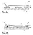
- Fig. 3a-b are diagrammatic side views of a MEM switch in open (signal isolation) and closed state (signal transmission). The drawings are not to scale.
- Fig. 3a-b show the MEM switch 40 in more detail and the function thereof.
- the switch 40 is typically fabricated on a substrate 41, provided with conductive contact layers 42, 44, the switching element 46, bias electrodes (not shown), conductive pads (not shown).
- the switching element 46 can for instance be fabricated as a metal layer operating such that when the switch is in its closed state, there is a path between the RF ports 42, 44 (See Fig. 3b). In its open state, the RF ports 42, 44 are separated by a distance, which is typically a few microns or the like.
- the beam 62 is pulled downwards by an electrostatic force, providing contact and closing the switch.
- a plurality of MEM switches are added along a delay line such that different transmission lengths (line paths) can be achieved, thereby realizing different corresponding phase shifts.
- a plurality of MEM switches are connected in close proximity to each other, for instance in series, forming different phase shift transmission path lengths to provide a phase switch device according to the invention, in which different phase shift values can be selected.
- the MEM switches 40 can be arranged in integrated circuits providing the phase switching device 20, or they can be provided directly on conventional PCBs to provide even lower cost.
- cellular phone is just one type of communication device having an antenna element in which the invention can be implemented. It can just as well be provided in other types of portable electronic equipments such as a lap top computer, a palm top computer, an electronic organizer, a smart-phone, a communicator.
Landscapes
- Transceivers (AREA)
- Waveguide Switches, Polarizers, And Phase Shifters (AREA)
- Variable-Direction Aerials And Aerial Arrays (AREA)
Abstract
- a first in-port (22) for an incoming RF signal, and a second out-port (24) for an outgoing RF signal;
- a phase switch device (20) including a plurality micro-electro-mechanical (MEM) switches (40) controllable by a control unit (30), said phase switch device (20) being arranged to select one of a plurality of phase shift values corresponding to a switchable time delay line having corresponding different selectable lengths, provided by the phase switch device (20) to the incoming RF signal.
Description
- This invention relates to phase shifting in RF applications, and in particular to phase shifting in a portable communication device. More particularly, the present invention relates to a phase shifter device and a portable communication device comprising the same.
- In a portable communication device, such as a cellular phone, comprising radiating elements (multiple band antennas etc), different frequencies (separate frequency bands or different frequencies within a band) might need to be phase shifted differently, for instance to optimize performance or to reduce radiation body losses (RF losses).
- A solution to this problem is for instance to provide so-called "delay lines" having different lengths, which requires a larger number of phase shifters. Typically, these phase shifters must be low cost, light in weight, have low power consumption etc. Besides that, a drawback is that phase shifters are normally bulky, which of course implies a problem since the space available on the PCB is limited. For instance, it could be impossible to find space for several delay lines, at least to a reasonable cost. Yet another drawback is that many components have to be measured and approved.
- Phase shifters typically comprise ferrites, PIN diodes and FET switch devices. Such devices are comparatively heavy, have comparatively high power consumption and are typically expensive. Moreover, PIN diodes and FET switches require DC bias voltage, which limits frequency performance and increase RF loss.
- Thus, there is a need to provide a phase shifter device which is capable of phase shifting different frequencies or frequency bands, which device is not bulky, does not have high power consumption, and which is cheap, such that requirements concerning weight, cost and performance are fulfilled.
- One object of the present invention is thus directed towards providing a phase shifter device, for a portable communication device, that is capable to phase shift different frequencies, such that requirements concerning weight, cost and performance are fulfilled.
- According to a principal aspect of the present invention, this object is achieved by a phase shifter device, in which micro-electro-mechanical switches MEM switches are added along a delay line.
- According to a first aspect of the present invention, there is provided a RF phase shifter device for a portable electronic communication device, said phase shifter device comprising:
- a phase switch device having a first in-port for an incoming RF signal, and a second out-port for an outgoing RF signal;
- including a plurality of micro-electro-mechanical (MEM) switches controllable by a control unit, said phase switch device being arranged to select one of a plurality of phase shift values ϕ corresponding to a switchable time delay line having corresponding different selectable lengths, provided by the phase switch device to the incoming RF signal.
- According to a second aspect of the present invention, including the first aspect, the control unit is provided by electronics.
- According to a third aspect of the present invention, inclduing the first aspect, the phase switch device is arranged to be controlled by software and electronics providing the control unit. In this way, the length of the phase shift can be set.
- A fourth aspect of the present invention includes any one of the previous aspects, wherein the MEM switches are metal-metal contact MEM switches.
- A fifth and sixth aspect of the present invention, includes any one of the first to the fourth aspects, wherein a plurality of switching devices are connected in series, or in parallel providing a set of selectable phase shifts to the RF signal(s).
- A seventh aspect of the present invention includes any one of the first to the fourth aspects, wherein a plurality of switching devices are connected in series, and in parallel providing a set of selectable phase shifts to the RF signal(s).
- Yet another aspect of the present invention includes any one of the previous aspects, wherein there is provided a portable electronic communication device comprising:
- a RF phase shifter device for a portable electronic communication device, said phase shifter device comprising:
- a phase switch device having a first in-port for an incoming RF signal, and a second out-port for an outgoing RF signal;
- including a plurality of micro-electro-mechanical (MEM) switches controllable by a control unit, said phase switch device being arranged to select one of a plurality of phase shift values ϕ corresponding to a switchable time delay line having corresponding different selectable lengths, provided by the phase switch device to the incoming RF signal.
- The phase shift can be controlled for each part of the frequency range that needs to be adjusted. Since the switching between different channels/bands are quite few compared to Rx/Tx switching, MEM switches would not have any problem handling this.
- The present invention has many advantages, one being that prior art devices are relatively heavier, consume more DC power and more expensive than the device according to the present invention, since the need of several phase shifters will be eliminated.
- It should be emphasized that the term "comprises/comprising" when used in this specification is taken to specify the presence of stated features, integers, steps or components, but does not preclude the presence or addition of one or more other features, integers, steps, components or groups thereof.
- The present invention will now be described in more detail in relation to the enclosed drawings, in which:
- Fig. 1 is a schematic and simplified diagram of an antenna element in a portable communication device coupled to a phase shifter device according to an aspect of the invention.
- Fig. 2 is a schematic electrical diagram of a MEM switch.
- Fig. 3a-3b are schematic side sectional views of an exemplary MEM switch in an open and closed state, respectively.
- Referring now to the drawings, a description will be given in detail of embodiments in accordance with the present invention.
- Fig. 1 shows a schematic and simplified diagram of an
antenna element 10 in a portable communication device coupled to aphase shifter device 1 according to an aspect of the invention. In this embodiment only oneantenna element 10 is shown, but without departing from the inventive idea,several antenna elements 10, arranged in any suitable manner such as a multi-band antenna, comprising several antenna elements, or the like, could also be provided (illustrated by a dashed line). Theantenna element 10 is connected to thephase shifter device 1, comprising aphase switch device 20, having a first in-port 22 for an incoming RF signal, and a second out-port 24 for an outgoing RF signal, whichphase switch device 20 comprises a plurality of micro-electro-mechanical switches (MEM switches) (not indicated in detail in this figure) added along a delay line, i. e. the MEM switches are integrated in thephase shifter device 1. The MEM switches can be connected in series, in parallel, or in any other suitable configuration. The employment of MEM switches reduces the number of phase shifters required to phase switch different frequencies. A control unit (CTRL) 30 provides control signals to thephase switch device 20, arranged to set a particular phase shift ϕ depending on the particular control signal, preferably embodied by means of suitable software combined with electronics. The phase shift ϕ can be controlled for each part of the frequency range that needs to be adjusted. - Since the switching between different channels/bands are quite few compared to Rx/Tx switching, the MEM switches (in the phase switch device 20) would have no problem handling this. By means of the invention, there will be no need of several bulky, power consuming phase shifters or many space consuming delay lines.
- In the embodiments described herein, the
phase switch device 20 comprising MEM switches employ MEM metal-metal switches known per se. Fig. 2 shows a schematic electrical diagram of aMEM switch 40, which is provided with afirst RF port 42, and asecond RF port 44, forming a RF line, and aswitching element 46 that can be closed to complete a path between the first andsecond port line 48 and line 49 (ground), which are connected to so-called "bias electrodes" (not shown in this figure; see Fig. 3). - There is a physical separation between the bias electrodes and the
RF ports - Typically, the surface area that the
MEM switch 40 requires on a printed circuit board (PCB) is very small (compared to a plurality of delay lines on a PCB), and typically require low DC control power to be operated. The MEM switches can be of any suitable type such as being made of GaAs, provided with metal layers that are conductive. Moreover, the MEM switches do not need bias voltage (and thereto necessary circuits) on the RF line. Fig. 3a-b are diagrammatic side views of a MEM switch in open (signal isolation) and closed state (signal transmission). The drawings are not to scale. - Fig. 3a-b show the
MEM switch 40 in more detail and the function thereof. Theswitch 40 is typically fabricated on asubstrate 41, provided withconductive contact layers switching element 46, bias electrodes (not shown), conductive pads (not shown). theswitching element 46 can for instance be fabricated as a metal layer operating such that when the switch is in its closed state, there is a path between theRF ports 42, 44 (See Fig. 3b). In its open state, theRF ports beam 62 is pulled downwards by an electrostatic force, providing contact and closing the switch. - According to the invention, a plurality of MEM switches are added along a delay line such that different transmission lengths (line paths) can be achieved, thereby realizing different corresponding phase shifts. Preferably, a plurality of MEM switches are connected in close proximity to each other, for instance in series, forming different phase shift transmission path lengths to provide a phase switch device according to the invention, in which different phase shift values can be selected.
- The MEM switches 40 can be arranged in integrated circuits providing the
phase switching device 20, or they can be provided directly on conventional PCBs to provide even lower cost. - It should be realised that cellular phone is just one type of communication device having an antenna element in which the invention can be implemented. It can just as well be provided in other types of portable electronic equipments such as a lap top computer, a palm top computer, an electronic organizer, a smart-phone, a communicator.
- There are more ways in which the invention can be varied. Therefore the invention is only to be limited by the accompanying claims.
Claims (8)
- A RF phase shifter device for a portable electronic communication device, said phase shifter device (1) comprising:a phase switch device (20) having a first in-port (22) for an incoming RF signal, and a second out-port (24) for an outgoing RF signal;
including a plurality of micro-electro-mechanical (MEM) switches (40) controllable by a control unit (30), said phase switch device (20) being arranged to select one of a plurality of phase shift values ϕ corresponding to a switchable time delay line having corresponding different selectable lengths, provided by the phase switch device (20) to the incoming RF signal. - The RF phase shifter device of claim 1, wherein the control unit (30) is provided by electronics.
- The RF phase shifter device of claim 1, wherein the control unit (30) is provided by software and electronics.
- The RF phase shifter device of any one of the previous claims, wherein said MEM switches (40) comprise metal-metal contact MEM switches.
- The RF phase shifter device of claim 1-4, wherein said MEM switches (40) are connected in series.
- The RF phase shifter device of claim 1-4, wherein said MEM switches (40) are connected in parallel.
- The RF phase shifter device of claim 1-4, wherein said MEM switches (40) are connected in series and in parallel.
- A portable electronic communication device comprising:a RF phase shifter device (1) for a portable electronic communication device, said phase shifter device (1) comprising:a phase switch device (20) having a first in-port (22) for an incoming RF signal, and a second out-port (24) for an outgoing RF signal;including a plurality of micro-electro-mechanical (MEM) switches (40) controllable by a control unit (30), said phase switch device (20) being arranged to select one of a plurality of phase shift values ϕ corresponding to a switchable time delay line having corresponding different selectable lengths, provided by the phase switch device (20) to the incoming RF signal.
Priority Applications (3)
| Application Number | Priority Date | Filing Date | Title |
|---|---|---|---|
| EP04021432A EP1635418A1 (en) | 2004-09-09 | 2004-09-09 | Phase shifter device including MEMS switches and delay lines and portable communication device using the same |
| PCT/EP2005/009183 WO2006027113A1 (en) | 2004-09-09 | 2005-08-25 | Phase shifter device including mems switches and delay lines and portable communication device using the same |
| TW094130982A TW200631230A (en) | 2004-09-09 | 2005-09-09 | Phase shifter device for a portable communication device |
Applications Claiming Priority (1)
| Application Number | Priority Date | Filing Date | Title |
|---|---|---|---|
| EP04021432A EP1635418A1 (en) | 2004-09-09 | 2004-09-09 | Phase shifter device including MEMS switches and delay lines and portable communication device using the same |
Publications (1)
| Publication Number | Publication Date |
|---|---|
| EP1635418A1 true EP1635418A1 (en) | 2006-03-15 |
Family
ID=34926475
Family Applications (1)
| Application Number | Title | Priority Date | Filing Date |
|---|---|---|---|
| EP04021432A Withdrawn EP1635418A1 (en) | 2004-09-09 | 2004-09-09 | Phase shifter device including MEMS switches and delay lines and portable communication device using the same |
Country Status (2)
| Country | Link |
|---|---|
| EP (1) | EP1635418A1 (en) |
| TW (1) | TW200631230A (en) |
Cited By (2)
| Publication number | Priority date | Publication date | Assignee | Title |
|---|---|---|---|---|
| US10608335B2 (en) | 2017-11-22 | 2020-03-31 | International Business Machines Corporation | RF signal switching, phase shifting and polarization control |
| US10680581B2 (en) | 2017-11-22 | 2020-06-09 | International Business Machines Corporation | RF signal switching, phase shifting and polarization control |
Citations (6)
| Publication number | Priority date | Publication date | Assignee | Title |
|---|---|---|---|---|
| EP1113524A2 (en) * | 1999-12-30 | 2001-07-04 | Nokia Mobile Phones Ltd. | Antenna structure, method for coupling a signal to the antenna structure, antenna unit and mobile station with such an antenna structure |
| US6281838B1 (en) * | 1999-04-30 | 2001-08-28 | Rockwell Science Center, Llc | Base-3 switched-line phase shifter using micro electro mechanical (MEMS) technology |
| US6310526B1 (en) * | 1999-09-21 | 2001-10-30 | Lap-Sum Yip | Double-throw miniature electromagnetic microwave (MEM) switches |
| US20020098613A1 (en) * | 2001-01-23 | 2002-07-25 | Hrl Laboratories, Llc | Monolithic single pole double throw rf mems switch |
| US20030137284A1 (en) * | 2002-01-23 | 2003-07-24 | Tyco Electronics Corporation | Switched reactance phase shifters |
| EP1361623A1 (en) * | 2002-05-08 | 2003-11-12 | Sony Ericsson Mobile Communications AB | Multiple frequency bands switchable antenna for portable terminals |
-
2004
- 2004-09-09 EP EP04021432A patent/EP1635418A1/en not_active Withdrawn
-
2005
- 2005-09-09 TW TW094130982A patent/TW200631230A/en unknown
Patent Citations (6)
| Publication number | Priority date | Publication date | Assignee | Title |
|---|---|---|---|---|
| US6281838B1 (en) * | 1999-04-30 | 2001-08-28 | Rockwell Science Center, Llc | Base-3 switched-line phase shifter using micro electro mechanical (MEMS) technology |
| US6310526B1 (en) * | 1999-09-21 | 2001-10-30 | Lap-Sum Yip | Double-throw miniature electromagnetic microwave (MEM) switches |
| EP1113524A2 (en) * | 1999-12-30 | 2001-07-04 | Nokia Mobile Phones Ltd. | Antenna structure, method for coupling a signal to the antenna structure, antenna unit and mobile station with such an antenna structure |
| US20020098613A1 (en) * | 2001-01-23 | 2002-07-25 | Hrl Laboratories, Llc | Monolithic single pole double throw rf mems switch |
| US20030137284A1 (en) * | 2002-01-23 | 2003-07-24 | Tyco Electronics Corporation | Switched reactance phase shifters |
| EP1361623A1 (en) * | 2002-05-08 | 2003-11-12 | Sony Ericsson Mobile Communications AB | Multiple frequency bands switchable antenna for portable terminals |
Cited By (2)
| Publication number | Priority date | Publication date | Assignee | Title |
|---|---|---|---|---|
| US10608335B2 (en) | 2017-11-22 | 2020-03-31 | International Business Machines Corporation | RF signal switching, phase shifting and polarization control |
| US10680581B2 (en) | 2017-11-22 | 2020-06-09 | International Business Machines Corporation | RF signal switching, phase shifting and polarization control |
Also Published As
| Publication number | Publication date |
|---|---|
| TW200631230A (en) | 2006-09-01 |
Similar Documents
| Publication | Publication Date | Title |
|---|---|---|
| JP4552205B2 (en) | Filter with switch function | |
| US9985331B2 (en) | Substrate integrated waveguide switch | |
| US6933893B2 (en) | Electronically tunable planar antenna and method of tuning the same | |
| US10163889B2 (en) | Phase shifter | |
| US11710903B2 (en) | Antenna-like matching component | |
| EP1505683B1 (en) | High frequency switch module and multi-layer substrate for high frequency switch module | |
| Fang et al. | 2.4-GHz absorptive MMIC switch for switched beamformer application | |
| JP5720854B2 (en) | Antenna matching device | |
| Qaroot et al. | Microfluidically reconfigurable reflection phase shifter | |
| EP3327859B1 (en) | Directional coupler and communication module | |
| EP2416330A1 (en) | Variable capacitance module and matching circuit module | |
| US10535927B2 (en) | Antenna system for metallized devices | |
| US20130147574A1 (en) | Non-reciprocal circuit element | |
| CN102138285A (en) | High-frequency switch module | |
| US20050231439A1 (en) | Antenna switch circuit, and composite high frequency part and mobile communication device using the same | |
| KR100848261B1 (en) | Device containing RF switch and RF switch | |
| EP1635418A1 (en) | Phase shifter device including MEMS switches and delay lines and portable communication device using the same | |
| WO2005022685A1 (en) | Antenna module for the high frequency and microwave range | |
| WO2006027113A1 (en) | Phase shifter device including mems switches and delay lines and portable communication device using the same | |
| JP4957095B2 (en) | Multiband high frequency amplifier | |
| CN118715722A (en) | Electronic equipment and communication systems | |
| Saripaka et al. | Realisation Aspects of SWaP Optimised RF Front End Using Multi-Function Modules | |
| KR101014472B1 (en) | Dense Multilayer Circuit | |
| KR20070110957A (en) | Front end module | |
| EP4213303A1 (en) | Antenna |
Legal Events
| Date | Code | Title | Description |
|---|---|---|---|
| PUAI | Public reference made under article 153(3) epc to a published international application that has entered the european phase |
Free format text: ORIGINAL CODE: 0009012 |
|
| AK | Designated contracting states |
Kind code of ref document: A1 Designated state(s): AT BE BG CH CY CZ DE DK EE ES FI FR GB GR HU IE IT LI LU MC NL PL PT RO SE SI SK TR |
|
| AX | Request for extension of the european patent |
Extension state: AL HR LT LV MK |
|
| 17P | Request for examination filed |
Effective date: 20060724 |
|
| 17Q | First examination report despatched |
Effective date: 20060921 |
|
| AKX | Designation fees paid |
Designated state(s): AT BE BG CH CY CZ DE DK EE ES FI FR GB GR HU IE IT LI LU MC NL PL PT RO SE SI SK TR |
|
| STAA | Information on the status of an ep patent application or granted ep patent |
Free format text: STATUS: THE APPLICATION IS DEEMED TO BE WITHDRAWN |
|
| 18D | Application deemed to be withdrawn |
Effective date: 20070201 |