EP1628351A1 - Piezoelectric material, manufacturing method thereof, and non-linear piezoelectric element - Google Patents
Piezoelectric material, manufacturing method thereof, and non-linear piezoelectric element Download PDFInfo
- Publication number
- EP1628351A1 EP1628351A1 EP04732788A EP04732788A EP1628351A1 EP 1628351 A1 EP1628351 A1 EP 1628351A1 EP 04732788 A EP04732788 A EP 04732788A EP 04732788 A EP04732788 A EP 04732788A EP 1628351 A1 EP1628351 A1 EP 1628351A1
- Authority
- EP
- European Patent Office
- Prior art keywords
- piezoelectric
- piezoelectric material
- ferroelectric
- point defects
- linear
- Prior art date
- Legal status (The legal status is an assumption and is not a legal conclusion. Google has not performed a legal analysis and makes no representation as to the accuracy of the status listed.)
- Withdrawn
Links
Images



Classifications
-
- H—ELECTRICITY
- H10—SEMICONDUCTOR DEVICES; ELECTRIC SOLID-STATE DEVICES NOT OTHERWISE PROVIDED FOR
- H10N—ELECTRIC SOLID-STATE DEVICES NOT OTHERWISE PROVIDED FOR
- H10N30/00—Piezoelectric or electrostrictive devices
- H10N30/80—Constructional details
- H10N30/85—Piezoelectric or electrostrictive active materials
- H10N30/853—Ceramic compositions
-
- H—ELECTRICITY
- H10—SEMICONDUCTOR DEVICES; ELECTRIC SOLID-STATE DEVICES NOT OTHERWISE PROVIDED FOR
- H10N—ELECTRIC SOLID-STATE DEVICES NOT OTHERWISE PROVIDED FOR
- H10N30/00—Piezoelectric or electrostrictive devices
- H10N30/80—Constructional details
- H10N30/85—Piezoelectric or electrostrictive active materials
- H10N30/853—Ceramic compositions
- H10N30/8536—Alkaline earth metal based oxides, e.g. barium titanates
-
- H—ELECTRICITY
- H10—SEMICONDUCTOR DEVICES; ELECTRIC SOLID-STATE DEVICES NOT OTHERWISE PROVIDED FOR
- H10N—ELECTRIC SOLID-STATE DEVICES NOT OTHERWISE PROVIDED FOR
- H10N30/00—Piezoelectric or electrostrictive devices
- H10N30/80—Constructional details
- H10N30/85—Piezoelectric or electrostrictive active materials
-
- H—ELECTRICITY
- H10—SEMICONDUCTOR DEVICES; ELECTRIC SOLID-STATE DEVICES NOT OTHERWISE PROVIDED FOR
- H10N—ELECTRIC SOLID-STATE DEVICES NOT OTHERWISE PROVIDED FOR
- H10N30/00—Piezoelectric or electrostrictive devices
- H10N30/01—Manufacture or treatment
- H10N30/04—Treatments to modify a piezoelectric or electrostrictive property, e.g. polarisation characteristics, vibration characteristics or mode tuning
-
- H—ELECTRICITY
- H10—SEMICONDUCTOR DEVICES; ELECTRIC SOLID-STATE DEVICES NOT OTHERWISE PROVIDED FOR
- H10N—ELECTRIC SOLID-STATE DEVICES NOT OTHERWISE PROVIDED FOR
- H10N30/00—Piezoelectric or electrostrictive devices
- H10N30/80—Constructional details
- H10N30/85—Piezoelectric or electrostrictive active materials
- H10N30/853—Ceramic compositions
- H10N30/8548—Lead-based oxides
- H10N30/8554—Lead-zirconium titanate [PZT] based
Definitions
- the invention of this application relates to a piezoelectric material and a piezoelectric element, and particularly, to a material of a non-linear piezoelectric characteristic which can be largely deformed at low voltage and an element using the material.
- the inventor of this application made a fundamental reexamination to the conventional piezoelectric materials.
- the following points are noted. That is, the inverse piezoelectric or electrostrain effect in the conventional material is due to the tiny shifts of ions, which causes slight change in crystalline lattice. Therefore, the resulting strain is extremely small.
- regions having different electric polarization directions (called domains) exist in the piezoelectric material.
- the polarization directions of domains may have angles of 180°, 90°, and the like depending on crystal symmetry. When an electric field is applied, domain switching occurs such that a polarization direction is changed to the field direction.
- an a-domain having polarization perpendicular to the electric field is converted into a c-domain such that polarization direction is along the electric field direction when the electric field is applied.
- the magnitude of the electrostrain obtained in this process is the length difference between the long and short axis.
- the magnitude can in principle reach as large as 1 % to 5 % depending on material.
- the value is tens of times as large as that obtained in a conventional piezoelectric effect.
- this giant electrostrain effect is generally irreversible, thus it is of little use.
- the inventor hereby provides a new way to develop non-linear piezoelectric material which can achieve a large and sharp deformation at low voltage and non-linear piezoelectric element, electric device or machine as an application of the non-linear piezoelectric element.
- the application provides the following inventions to solve the above problems.
- the invention of this application is derived by utilizing his fundamental finding about the symmetry-conforming nano-ordering of point defects (Xiaobing Ren and Kazuhiro Otuka PHYSICAL REVIEW LETTERS Vol. 85, No. 5, 2000 July 31, pp. 1016 to 1019), which makes domain switching reversible, thereby a giant electrostrain effect can be obtained. More specifically, the invention of this application is accomplished as a novel technical idea based on a novel technical knowledge.
- FIG. 1 is a schematic two-dimensional diagram showing the principle of symmetry-conforming property of point defects in the crystal structure of a piezoelectric material of the invention of this application.
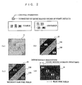
- FIG. 2 also explains a method of manufacturing a piezoelectric material of the invention of this application.
- ferroelectric materials containing non-180° domains In order to obtain a larger deformation, it is preferably to use ferroelectric materials containing non-180° domains.
- the low-symmetry ferroelectric materials shown in FIGs. 2(b) and 2(c) contain a large number of non-180° twin-related domains 22A and 22B : 23A and 23B.
- the crystal structure may be single crystalline or polycrystalline.
- the shape of the crystal may be a bulk or a thin film.
- the shape may also be a multilayered film.
- the various crystal structures and shapes may be formed by conventionally known techniques. For example, various means of liquid-phase methods or vapor-phase methods may be employed to make thin films or multilayered films.
- a ferroelectric material constituting a piezoelectric material of the invention of this application is not limited in composition.
- a conventionally known ABO 3 -type composite oxide or a material obtained by adding another element (ion) to the oxide is preferably considered.
- ABO 3 -type composite oxide not only BaTiO 3 -type material and (Ba, Sr) TiO 3 -type material, but also Pb(Zr, Ti)O 3 -type material, (Pb, La)(Zr, Ti)O 3 -type material, and the like are known. Any material containing one of these materials as a major component and having a piezoelectric function may be used. A mixture of the material and other element may be used, or an inevitable impurity may also produce the same effect.
- a lead-free piezoelectric material and a lead-free piezoelectric element can also be provided without using Pb (lead) which is not preferable for human health or environment.
- At least one of an alkali metal, an alkali-earth metal, and a transition metal may be used.
- an alkali metal for example, at least one of Na, K, Mg, Ca, Al, V, Cr, Mn, Fe, Co, Ni, Zn, Ga, Rb, Y, Zr, Nb, Mo, Ru, Rh, Ag, Sn, Hf, Ta, W, Os, Ir, Pt, Pb, Bi, and a rare-earth element may be used.
- BaTiO 3 : BT, (Ba, Sr)TiO 3 : BST, ferroelectric materials added with at least one of alkali metals such as K, Na, and Rb, Fe, and Mn in these materials, Pb(Zr, Ti)O 3 : PZT, (Pb, La)(Zr, Ti)O 3 : PLZT, and materials added with other element in these materials may be exemplified.
- a molar ratio may be generally set at 20 mol% or less.
- Mn-added BT BaTiO 3 (containing Mn at 10 mol% or less) or Mn-added BST : (Ba, Sr)TiO 3 (containing Mn at 10 mol% or less, and Sr/Ba atomic ratio is 0.5 or less) may be exemplified.
- a giant piezoelectric deformation electrostrain can be generated at lower voltage.
- the piezoelectric material of the invention of this application is very useful and advantageous to applications to various sensors such as acceleration sensor, knocking sensor, and AE sensor, various electric devices and machines such as ultrasonic microphone, piezoelectric loudspeaker, piezoelectric actuator, ultrasonic motor, printer head, gun for an ink-jet printer, or parts of the sensors, the devices, and the machines.
- various sensors such as acceleration sensor, knocking sensor, and AE sensor
- various electric devices and machines such as ultrasonic microphone, piezoelectric loudspeaker, piezoelectric actuator, ultrasonic motor, printer head, gun for an ink-jet printer, or parts of the sensors, the devices, and the machines.
- BaTiO 3 single crystal was fabricated by a flux method, cooled, and then subjected to an aging treatment below Curie temperature (at 80°C for three days).
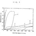
- An electric field - deformation characteristic of the obtained piezoelectric material is shown as curve d in FIG. 3.
- deformation characteristics of the conventional piezoelectric materials are shown as curves a, b, and c, respectively.
- the piezoelectric material of the invention of this application can realize reversible domain switching at low electric field, and the piezoelectric material exhibits a giant non-linear piezoelectric effect,
- the deformation has a magnitude that is approximately tens of times as large as that of each of the conventional resultant piezoelectric deformations (curves a to c in FIG. 3) at the same electric field of a popularly used PZT piezoelectric element. Furthermore, it is understood that the deformation is steep and has a non-linear characteristic.
- the resultant (BaK)TiO 3 single crystal was cooled and then subjected to an aging treatment below Curie temperature (at room temperature of 18°C to 22°C for one month).
- the piezoelectric material does not use toxic lead, the piezoelectric material is environment-friendly.
- PLZT ceramic piezoelectric material of the invention of this application exhibits a deformation magnitude which is several times as large as that of a conventional material at low voltage. Also, in Mn-BST and Mn-BT, reversible deformation occurs. Since the materials do not contain toxic lead, the materials are promising in view of environment.
- Microscopy images obtained by observing crystal states A to J in FIG. 5 are shown in FIG. 6.
- BaTiO 3 Fe-BT single crystal containing 0.02 at% of Fe was manufactured and subjected to an aging treatment at a temperature of 80°C for 5 days. The resultant material was measured in electric field - piezoelectric deformation characteristic. As a result, a giant reversible deformation of 0.75 % was obtained at low electric field of 200 V/mm. This value is 40 times as large as an electrostrain obtained by the conventional PZT. The value is also 10 or more times as large as electrostrain obtained by a recent PZN-PT single crystal.
- a giant deformation can be realized at low electric field. Furthermore, a new piezoelectric material having a non-linear characteristic in which the deformation steeply increases at a critical electric field, a piezoelectric element and an electric device or machine using the piezoelectric material, and parts for the element and the device or machine are provided.
Landscapes
- Engineering & Computer Science (AREA)
- Chemical & Material Sciences (AREA)
- Ceramic Engineering (AREA)
- Manufacturing & Machinery (AREA)
- Compositions Of Oxide Ceramics (AREA)
- Crystals, And After-Treatments Of Crystals (AREA)
Abstract
A piezoelectric material is provided that has mobile point defects which are arranged so that the short-range order symmetry is matched with the crystal symmetry of the ferroelectric phase. A large non-linear electrostrain effect is obtained by the reversible domain switching under electric field in the ferroelectric material. Thus, it is possible to provide a piezoelectric material and its element having a large and steep deformation even at low voltage. Its manufacturing method is also disclosed.
Description
- The invention of this application relates to a piezoelectric material and a piezoelectric element, and particularly, to a material of a non-linear piezoelectric characteristic which can be largely deformed at low voltage and an element using the material.
- As methods of obtaining deformation by an electric field, the following two methods are known.
- (1) A ferroelectric phase of a ferroelectric material is subjected to a "poling" process to obtain an approximately linear piezoelectric effect (deformation by electric field). As a characteristic feature of this method, domains of the ferroelectric material fixed by the poling process (i.e., the domains are not rotated), positive and negative ions in a crystal are moved by application of the electric field to obtain the linear piezoelectric deformation. Pb(ZrTi)O3 (PZT) serving as a typical piezoelectric material obtains piezoelectric effect by using the method. This is a so-called poled PZT ceramics [soft type (see curve a in the accompanying drawing in FIG. 3) and hard type (see curve b in FIG. 3)].
- (2) Non-linear piezoelectric effect is obtained by using electric field induced phase transition of an antiferroelectric material. As a characteristic feature of this method, a strong electric field is applied to an antiferroelectric material so as to change its state into a ferroelectric state, thereby obtaining non-linear deformation [A typical example of this type is shown as curve c in FIG. 3, which shows the non-linear electrostrain during an electric field induced antiferroelectric material - dielectric material phase transition in PNZST ceramics].
- As any one of the above methods, with respect to a piezoelectric material which achieves a deformation by electric field and a piezoelectric element using the piezoelectric material, in recent years, with rapidly expanding application to sensors such as acceleration sensor, knocking sensor, or AE sensor, ultrasonic microphone, piezoelectric loudspeaker, piezoelectric actuator, ultrasonic motor, printer head, gun for ink-jet printer, and the like, a high conversion efficiency is required in application to the actuator or the sensor. In particular, with respect to the actuator which converts a voltage into deformation, the actuator which can produce a large stroke (deformation) at low voltage is required. In addition, the deformation is desired to be non-linear (for example, a deformation sharply increases at a critical voltage). However, in the conventional technique described above, the following problems have been posed.
- For example, in the conventional technique described in item (1) (see curves a and b in FIG. 3), <1> a deformation is small at low voltage (only a deformation of 0.01 % to 0.1% occurs at an electric field of 1000 V/mm). <2> A deformation is almost linear with electric field. <3> A poling process is required in an electrode direction.
- In the conventional technique described in item (2) (see the curve c in FIG. 3), <1> a drive electric field is large (> 2500 V/mm). <2> The maximum deformation is small (0.01 % to 0.08 %). <3> The characteristic has the disadvantage of being very sensitive to temperature.
- The inventor of this application made a fundamental reexamination to the conventional piezoelectric materials. In this case, the following points are noted. That is, the inverse piezoelectric or electrostrain effect in the conventional material is due to the tiny shifts of ions, which causes slight change in crystalline lattice. Therefore, the resulting strain is extremely small. On the other hand, it is noticed that regions having different electric polarization directions (called domains) exist in the piezoelectric material. The polarization directions of domains may have angles of 180°, 90°, and the like depending on crystal symmetry. When an electric field is applied, domain switching occurs such that a polarization direction is changed to the field direction. For example, an a-domain having polarization perpendicular to the electric field is converted into a c-domain such that polarization direction is along the electric field direction when the electric field is applied. With this domain switching, the long-axis direction and the short-axis direction of the low symmetry ferroelectric phase are exchanged. The magnitude of the electrostrain obtained in this process is the length difference between the long and short axis. The magnitude can in principle reach as large as 1 % to 5 % depending on material. The value is tens of times as large as that obtained in a conventional piezoelectric effect. However, this giant electrostrain effect is generally irreversible, thus it is of little use.
- However, the inventor noticed a way that can make the domain switching reversible, so that it makes possible to obtain a giant recoverable electrostrain effect.
- On the basis of new principle, the inventor hereby provides a new way to develop non-linear piezoelectric material which can achieve a large and sharp deformation at low voltage and non-linear piezoelectric element, electric device or machine as an application of the non-linear piezoelectric element.
- The application provides the following inventions to solve the above problems.
- [1] A piezoelectric material which is a ferroelectric having mobile point defects, wherein the mobile point defects are arranged such that the symmetry of short-range order of the point defects coincides with the crystal symmetry of the ferroelectric phase. Such piezoelectric material exhibits a characteristic non-linear piezoelectric effect caused by reversible switching of domains under electric field.
- [2] The piezoelectric material is characterized by the existence of vacancies as the mobile point defects in a ferroelectric material. Such defects are either introduced by chemical equilibrium or addition of dopant(s).
- [3] The piezoelectric material described in any one of the above items is subject to an aging treatment at a temperature below Curie temperature, and the point defecst are arranged such that the symmetry of the short-range order of the point defects coincides with the crystal symmetry of the ferroelectric phase.
- [4] The piezoelectric material described in any one of the above items, wherein the piezoelectric material is a single crystal or a polycrystal.
- [5] The piezoelectric material described in any one of the above items, wherein the piezoelectric material is a thin film.
- [6] The piezoelectric material described in any one of the above items, wherein the piezoelectric material is a multilayer film.
- [7] The piezoelectric material described in any one of the above items, wherein the ferroelectric material is ABO3-type ferroelectric material.
- [8] The piezoelectric material described in any one of the above items, wherein the ferroelectric material is BaTiO3, (Ba, Sr)TiO3-type ferroelectric material.
- [9] The piezoelectric material described in any one of the above items, wherein the ferroelectric material is Pb(Zr, Ti)O3 or (Pb, rare-earth element)(Zr, Ti)O3-type ferroelectric material.
- [10] The piezoelectric material described in any one of the above items, wherein other element is added.
- [11] The piezoelectric material described in any one of the above items, wherein the other element is at least one element of an alkali metal, an alkali-earth metal, and a transition metal.
- [12] The piezoelectric material described in any one of the above items, wherein the other element is added by 20 mol % or less.
- [13] The piezoelectric material described in any one of the above, wherein the other element is at least one of Na, K, Mg, Ca, Al, V, Cr, Mn, Fe, Co, Ni, Zn, Ga, Rb, Sr, Y, Zr, Nb, Mo, Ru, Rh, Ag, Sn, Hf, Ta, W, Os, Ir, Pt, Pb, Bi, and a rare-earth element.
- [14] A piezoelectric material exhibiting a non-linear piezoelectric effect, wherein the piezoelectric material is at least one of ABO3-type ferroelectric material and a ferroelectric material obtained by adding other element to ABO3-type ferroelectric material, and wherein the piezoelectric material has been subjected to an aging treatment at a temperature below Curie temperature.
- [15] The piezoelectric material exhibiting the non-linear piezoelectric effect, wherein the piezoelectric material is at least one of BaTiO3, (Ba, Sr)TiO3, and a ferroelectric material obtained by adding at least one of K, Fe, and Mn to BaTiO3 or (Ba, Sr)TiO3.
- [16] The piezoelectric material exhibiting the non-linear piezoelectric effect, wherein the piezoelectric material is (Pb, La)(Zr, Ti)O3 ferroelectric material.
- [17] A method of manufacturing a piezoelectric material described in any one of the above items, including steps of: introducing mobile point defects in a ferroelectric material; and arranging the point defects such that the symmetry of short-range order of the mobile point defects coincides with the crystal symmetry of the ferroelectric phase, and wherein the ferroelectric material exhibits a non-linear piezoelectric effect by reversible switching of domains thereof under electric field.
- [18] A method of manufacturing a piezoelectric material exhibiting a non-linear piezoelectric effect, wherein at least one of ABO3-type ferroelectric material and a ferroelectric material obtained by adding other element to ABO3-type ferroelectric material is subjected to an aging treatment at a temperature below Curie temperature.
- [19] The method of manufacturing a piezoelectric material, wherein the piezoelectric material is at least one of BaTiO3, (Ba, Sr)TiO3, and a ferroelectric material obtained by adding at least one of K, Fe, and Mn to BaTiO3 or (Ba, Sr)TiO3.
- [20] The method of manufacturing a piezoelectric material, wherein the piezoelectric material is (Pb, La)(Zr, Ti)O3 ferroelectric material.
- [21] A non-linear piezoelectric element wherein one or more of the piezoelectric materials constitutes the non-linear piezoelectric element.
- [22] An electric device or machine or parts thereof, wherein a non-linear piezoelectric element is incorporated as at least a part of a configuration.
- [23] An electric device or machine or parts thereof, wherein any one of the piezoelectric materials is used as at least a part of the configuration of the electric device or machine or parts thereof.
- As described above, the invention of this application is derived by utilizing his fundamental finding about the symmetry-conforming nano-ordering of point defects (Xiaobing Ren and Kazuhiro Otuka PHYSICAL REVIEW LETTERS Vol. 85, No. 5, 2000 July 31, pp. 1016 to 1019), which makes domain switching reversible, thereby a giant electrostrain effect can be obtained. More specifically, the invention of this application is accomplished as a novel technical idea based on a novel technical knowledge.
-
- FIG. 1 is a schematic two-dimensional diagram showing the principle of the symmetry-conforming property of point defects in the crystal structure of a piezoelectric material according to the invention of this application.
- FIG. 2 is a schematic diagram for explaining formation of a piezoelectric material which exhibits a giant non-linear piezoelectric effect of the invention of this application.
Reference numerals and symbols in FIGs. 1 and 2 denote the followings:- B point defect (site 0)
- 1 to 4 sites neighboring point defect B (at site 0)
- P probability of finding another defect near site 0 (occupied by point defect B) in equilibrium
- 11,14 symmetry of short-range order of point defects
- 12, 13 crystal symmetry
- 21 ferroelectric material in paraelectric state (above Curie temperature)
- 22 ferroelectric material including a domain in which symmetry of short-range order of point defects does not coincide with crystal symmetry
- 22A, 22B, 23A, 23B twin-related domains
- 23 ferroelectric material including a domain in which symmetry of short-range order of point defects coincides with crystal symmetry
- 24 the state obtained when an electric field is applied to the ferroelectric material in
state 23
- FIG. 3 is a figure (compared with conventional technique) showing an electric field - deformation characteristic of the piezoelectric material of the invention of this application.
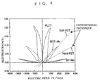
- FIG. 4 is a graph showing another electric field - deformation characteristic of the invention of this application.
- FIG. 5 is a graph showing a voltage - polarization characteristic obtained by reversible domain switching in a voltage cycle with respect to the piezoelectric material of the invention of this application.
- FIG. 6 is an optical microscopy photograph showing reversible switching of domains of the piezoelectric material in accordance with FIG. 5.
- The invention of this application has the characteristic features described above. The invention of this application will be described below in detail.
- FIG. 1 is a schematic two-dimensional diagram showing the principle of symmetry-conforming property of point defects in the crystal structure of a piezoelectric material of the invention of this application.
- The following description will be given with reference to FIG. 1.
- (1) In the invention of this application, a ferroelectric material has mobile points defects. The "ferroelectric material" mentioned here is defined as a "material having spontaneous polarization which can be switched by an external electric field". A "point defect" means, in the invention of this application, a defective lattice site, a vacancy, or a dopant (ion) in a crystal.
As methods of introducing point defects in a ferroelectric material, two typical methods are considered, for example.- <1> Point defects (oxygen vacancies or the like) are naturally generated by chemical equilibrium during the processing procedure (crystal growth, high-temperature sintering, heat treatment, and the like) for manufacturing an element.
- <2> Point defects are introduced by doping (ion). For example, ions having different valences are doped in A-site or B-site of ABO3-type ferroelectric material to introduce point defects such as oxygen vacancy, A vacancy, and B vacancy.
With the introduction of the point defects, when the probability of finding another defect occupying region around a certain point defect (nanometer region) is considered, as having been reported by the inventor, the occupation probability shows a symmetry that coincides with symmetry of the crystal in equilibrium. This is called symmetry-conforming principle of a nano-ordering of point defects.
According to the symmetry principle, in a paraelectric state (above Curie temperature) of a ferroelectric material in FIG. 1(a), reference symbol B denotes a point defect (at site 0),reference numerals 1 to 4 denote sites neighboring the point defect B (at site 0), and reference symbol P (shaded regions in FIG. 1(a)) denotes a probability of finding other defects in thesites 1 to 4 neighboring the site 0 (occupied by point defect B) in equilibrium. In such a case, the probabilities P at these sites are given by P1 B = P2 B = P3 B = P4 B, i.e., are equal to each other. More specifically, a stable state in whichsymmetry 11 of short-range order of the point defects coincides withcrystal symmetry 12 is established.
Therefore, point defect symmetry is high in a paraelectric phase. Similarly, the symmetry (in equilibrium) of point defects in a ferroelectric phase follows crystal symmetry, and at the same time, point defect polarization caused by the point defects coincides with the spontaneous polarization.
When the material is cooled (without diffusion), ferroelectric transformation to a state shown in FIG. 1(b) occurs. At this time, the probabilities P at thesites 1 to 4 are kept at P1 B = P2 B = P3 R = P4 B. However, in this case, thesymmetry 11 of the short-range order of point defects does not coincide withcrystal symmetry 13 is established, thus it is an unstable state.
Therefore, upon cooling paraelectric phase of the piezoelectric material changes into a ferroelectric phase with low crystal symmetry. At this time, the symmetry of the point defects in ferroelectric state inherits that in the paraelectric phase, and thus it is an unstable state. - (2) Therefore, in a piezoelectric material of the invention of this application, as shown in FIG.1(c), the probabilities in the
sites 1 to 4 are given by P1 B = P2 B≠ P3 B≠ P4 B, so thatsymmetry 14 of short-range order of point defects is changed to follow thecrystal symmetry 13. This state is the most stable state. The coincidence of the symmetries is made possible by an aging treatment for example. The aging treatment should be done at a temperature below Curie temperature. The aging time is dependent on an aging temperature. In general, the aging time is desirably one day or longer. When the aging treatment is performed at a predetermined temperature, the state is gradually saturated, and there is little further change with prolonged aging. - The coincidence between the symmetries, i.e., the symmetry of the short-range order of the mobile point defects is made to coincide with the symmetry of the crystal in the ferroelectric phase. This provides a piezoelectric material with a non-linear electrostrain effect obtained by reversible domain switching under electric field in the invention of this application.
- Next, realization of giant electrostrain under the electric field by reversible domain switching will be described below by FIG. 2. FIG. 2 also explains a method of manufacturing a piezoelectric material of the invention of this application.
- (1) A
ferroelectric material 21 in a paraelectric state in FIG. 2(a) is prepared. Thematerial 21 has a stable state in which thesymmetry 11 of the short-range order of the point defects coincides with thecrystal symmetry 12, as shown in FIG. 1(a). - (2) The
ferroelectric material 21 in FIG. 2(a) is cooled to obtain aferroelectric material 22 including domains in FIG. 2(b) by the transformation of the ferroelectric material. Theferroelectric material 22 is set in an unstable state in which thesymmetry 11 of the short-range order of the point defects does not coincide with thecrystal symmetry 13, as shown in FIG. 1(b). - (3) The
ferroelectric material 22 in FIG. 2(b) is subjected to an aging treatment to obtain aferroelectric material 23 shown in FIG. 2(c), which includes domains in whichsymmetry 14 of short-range order of point defects is made to coincide with thecrystal symmetry 13, as shown in FIG. 1(c), Theferroelectric material 23 is now set in the most stable state, and corresponds to a piezoelectric material of the invention of this application. - (4) Therefore, as shown in FIG. 2(d), when an electric field is applied to the domain of the
ferroelectric material 23 including the domain as shown in FIG. 2(c) and then removed, the domain of the ferroelectric phase subjected to the aging treatment is reversibly switched according to the application and removal of the electric field. More importantly, a larger piezoelectric deformation: electrostrain is generated by the switching.Reference numeral 24 in FIG. 2(d) shows a state obtained when the electric field is applied to theferroelectric material 23 shown in FIG. 2(c) [in FIG. 2(d), the shape indicated by the dotted line shows the shape before the electric field shown in FIG. 2(c) is applied]. - In order to obtain a larger deformation, it is preferably to use ferroelectric materials containing non-180° domains. The low-symmetry ferroelectric materials shown in FIGs. 2(b) and 2(c) contain a large number of non-180° twin-related
domains - With respect to the piezoelectric material of the invention of this application which exhibits the piezoelectric deformation as described above, the crystal structure may be single crystalline or polycrystalline. The shape of the crystal may be a bulk or a thin film. The shape may also be a multilayered film. The various crystal structures and shapes may be formed by conventionally known techniques. For example, various means of liquid-phase methods or vapor-phase methods may be employed to make thin films or multilayered films.
- A ferroelectric material constituting a piezoelectric material of the invention of this application is not limited in composition. However, a conventionally known ABO3-type composite oxide or a material obtained by adding another element (ion) to the oxide is preferably considered. As typical examples of ABO3-type composite oxide, not only BaTiO3-type material and (Ba, Sr) TiO3-type material, but also Pb(Zr, Ti)O3-type material, (Pb, La)(Zr, Ti)O3-type material, and the like are known. Any material containing one of these materials as a major component and having a piezoelectric function may be used. A mixture of the material and other element may be used, or an inevitable impurity may also produce the same effect.
- With respect to these ferroelectric materials, in the invention of this application, mobile point defects are arranged. As in a piezoelectric material consisting of BaTiO3, (Ba, Sr)TiO3, or a compound obtained by adding other element (ion) to these compounds, in the invention of this application, a lead-free piezoelectric material and a lead-free piezoelectric element can also be provided without using Pb (lead) which is not preferable for human health or environment.
- When elements (ions) to be added are used, as these elements, at least one of an alkali metal, an alkali-earth metal, and a transition metal may be used. For example, at least one of Na, K, Mg, Ca, Al, V, Cr, Mn, Fe, Co, Ni, Zn, Ga, Rb, Y, Zr, Nb, Mo, Ru, Rh, Ag, Sn, Hf, Ta, W, Os, Ir, Pt, Pb, Bi, and a rare-earth element may be used.
- More specifically, BaTiO3 : BT, (Ba, Sr)TiO3 : BST, ferroelectric materials added with at least one of alkali metals such as K, Na, and Rb, Fe, and Mn in these materials, Pb(Zr, Ti)O3 : PZT, (Pb, La)(Zr, Ti)O3 : PLZT, and materials added with other element in these materials may be exemplified.
- When the element is added, it is preferably considered that a molar ratio may be generally set at 20 mol% or less. In particular, as a piezoelectric material added with the element, Mn-added BT : BaTiO3 (containing Mn at 10 mol% or less) or Mn-added BST : (Ba, Sr)TiO3 (containing Mn at 10 mol% or less, and Sr/Ba atomic ratio is 0.5 or less) may be exemplified.
- According to the piezoelectric materials of the invention of this application, a giant piezoelectric deformation: electrostrain can be generated at lower voltage.
- For this reason, the piezoelectric material of the invention of this application is very useful and advantageous to applications to various sensors such as acceleration sensor, knocking sensor, and AE sensor, various electric devices and machines such as ultrasonic microphone, piezoelectric loudspeaker, piezoelectric actuator, ultrasonic motor, printer head, gun for an ink-jet printer, or parts of the sensors, the devices, and the machines.
- Therefore, examples will be described in more details. The invention is, of course, not limited to the following examples.
- BaTiO3 single crystal was fabricated by a flux method, cooled, and then subjected to an aging treatment below Curie temperature (at 80°C for three days). An electric field - deformation characteristic of the obtained piezoelectric material is shown as curve d in FIG. 3. In FIG. 3, as described above, deformation characteristics of the conventional piezoelectric materials are shown as curves a, b, and c, respectively.
- As is apparent from the curve d in FIG. 3, the piezoelectric material of the invention of this application can realize reversible domain switching at low electric field, and the piezoelectric material exhibits a giant non-linear piezoelectric effect,
- By rearrangement of a small number of oxygen vacancies (point defects) naturally included in BaTiO3 single crystal by the aging treatment (symmetry of short-range order of point defects is made to coincide with crystal symmetry), a giant piezoelectric deformation of about 0.5% can be obtained at low electric field (200 V/mm).
- The deformation has a magnitude that is approximately tens of times as large as that of each of the conventional resultant piezoelectric deformations (curves a to c in FIG. 3) at the same electric field of a popularly used PZT piezoelectric element. Furthermore, it is understood that the deformation is steep and has a non-linear characteristic.
- (BaK)TiO3 single crystal added with a small amount of K (0.7 mol%) was fabricated by a flux method.
- The resultant (BaK)TiO3 single crystal was cooled and then subjected to an aging treatment below Curie temperature (at room temperature of 18°C to 22°C for one month).
- In this case, point defects were generated by addition of K ions, the aging treatment was performed below Curie temperature to cause the symmetry of short-range order of the point defects to coincide with the crystal symmetry. An electrostrain characteristic of the obtained piezoelectric material is indicated by curve e in FIG. 3.
- According to the curve e in FIG. 3, a large piezoelectric deformation of 0.52 % is obtained at an electric field of 1470 V/mm. This deformation is very large in comparison with the results (curves a to c in FIG. 3) at the same electric field in a popularly used conventional PZT piezoelectric element. Furthermore, it is understood that the deformation is steep and that the piezoelectric material has a non-linear characteristic.
- In addition, since the piezoelectric material does not use toxic lead, the piezoelectric material is environment-friendly.
- The next three ceramics (polycrystal) samples were prepared as piezoelectric materials of the invention of this application.
- 1) (Pb, La)(Zr, Ti)O3 = PLZT ceramics was subjected to an aging treatment at room temperature (without polarization) for 30 days.
- 2) Mn-(Ba, Sr)TiO3 : Mn-BST (containing Mn at 1 mol%) ceramics was subjected to an aging treatment at 70°C for 5 days.
- 3) Mn-BaTiO3 : Mn-BT (containing Mn at 1 mol%) ceramics was subjected to an aging treatment at room temperature for 3 months.
- With respect to the above three ceramics piezoelectric materials, electric field - deformation characteristics were measured. The results are shown in FIG. 4.
- For comparison, measurement results of conventional hard PZT and soft PZT are also shown in FIG. 4.
- As is apparent from FIG. 4, PLZT ceramic piezoelectric material of the invention of this application exhibits a deformation magnitude which is several times as large as that of a conventional material at low voltage. Also, in Mn-BST and Mn-BT, reversible deformation occurs. Since the materials do not contain toxic lead, the materials are promising in view of environment.
- With respect to Mn-BT ceramics in Example 3, electric field - polarization characteristics were measured with a voltage cycle of 0 V, 800 V, -800 V, and 0 V. The results are shown in FIG. 5.
- Microscopy images obtained by observing crystal states A to J in FIG. 5 are shown in FIG. 6.
- From FIGS. 5 and 6, generation of reversible switching of ferroelectric domains in the piezoelectric material of the invention of this application is confirmed.
- BaTiO3 : Fe-BT single crystal containing 0.02 at% of Fe was manufactured and subjected to an aging treatment at a temperature of 80°C for 5 days. The resultant material was measured in electric field - piezoelectric deformation characteristic. As a result, a giant reversible deformation of 0.75 % was obtained at low electric field of 200 V/mm. This value is 40 times as large as an electrostrain obtained by the conventional PZT. The value is also 10 or more times as large as electrostrain obtained by a recent PZN-PT single crystal.
- As has been described above in detail, according to the invention of this application, a giant deformation can be realized at low electric field. Furthermore, a new piezoelectric material having a non-linear characteristic in which the deformation steeply increases at a critical electric field, a piezoelectric element and an electric device or machine using the piezoelectric material, and parts for the element and the device or machine are provided.
Claims (23)
- A piezoelectric material which is a ferroelectric and piezoelectric having mobile point defects, wherein the mobile point defects are arranged such that the symmetry of short-range order of the point defects coincides with the crystal symmetry of the ferroelectric phase, and the piezoelectric material exhibits a non-linear piezoelectric effect by reversible switching of domains under electric field.
- The piezoelectric material according to claim 1, wherein the mobile point defects are vacancies of an element constituting the ferroelectric material introduced by either chemical equilibrium or doping.
- The piezoelectric material according to claim 1 or 2, wherein the piezoelectric material is subject to an aging treatment at a temperature below Curie temperature, and the point defects are arranged such that the symmetry of the short-range order of the point defects coincides with the crystal symmetry of the ferroelectric phase.
- The piezoelectric material according to any one of claims 1 to 3, wherein the piezoelectric material is a single crystal or a polycrystal.
- The piezoelectric material according to any one of claims 1 to 3, wherein the piezoelectric material is a thin film.
- The piezoelectric material according to claim 5, wherein the piezoelectric material is a multilayer film.
- The piezoelectric material according to any one of claims 1 to 6, wherein the ferroelectric material is ABO3-type ferroelectric material.
- The piezoelectric material according to claim 7, wherein the ferroelectric material is BaTiO3, (Ba, Sr)TiO3-type ferroelectric material.
- The piezoelectric material according to claim 7, wherein the ferroelectric material is Pb(Zr, Ti)O3 or (Pb, rare-earth element)(Zr, Ti)O3-type ferroelectric material.
- The piezoelectric material according to any one of claims 7 to 9, wherein other element is added.
- The piezoelectric material according to claim 10, wherein the other element is at least one element of an alkali metal, an alkali-earth metal, and a transition metal.
- The piezoelectric material according to claim 8 or 9, wherein the other element is added by 20 mol % or less.
- The piezoelectric material according to any one of claims 10 to 12, wherein the other element is at least one of Na, K, Mg, Ca, Al, V, Cr, Mn, Fe, Co, Ni, Zn, Ga, Rb, Sr, Y, Zr, Nb, Mo, Ru, Rh, Ag, Sn, Hf, Ta, W, Os, Ir, Pt, Pb, Bi, and a rare-earth element.
- A piezoelectric material exhibiting a non-linear piezoelectric effect, wherein the piezoelectric material is at least one of ABO3-type ferroelectric material and a ferroelectric material obtained by adding other element to ABO3-type ferroelectric material, and wherein the piezoelectric material has been subjected to an aging treatment at a temperature below Curie temperature.
- The piezoelectric material exhibiting the non-linear piezoelectric effect according to claim 14, wherein the piezoelectric material is at least one of BaTiO3, (Ba, Sr)TiO3, and a ferroelectric material obtained by adding at least one of K, Fe, and Mn to BaTiO3 or (Ba, Sr)TiO3.
- The piezoelectric material exhibiting the non-linear piezoelectric effect according to claim 14, wherein the piezoelectric material is (Pb, La)(Zr, Ti)O3 ferroelectric material.
- A method of manufacturing a piezoelectric material according to any one of claims 1 to 13, comprising steps of:(a) introducing mobile point defects in a ferroelectric material; and(b) arranging the point defects such that the symmetry of short-range order of the mobile point defects coincides with the crystal symmetry of the ferroelectric phase,
and wherein the ferroelectric material exhibits a non-linear piezoelectric effect by reversible switching of domains thereof under electric field. - A method of manufacturing a piezoelectric material exhibiting a non-linear piezoelectric effect, wherein at least one of ABO3-type ferroelectric material and a ferroelectric material obtained by adding other element to ABO3-type ferroelectric material is subjected to an aging treatment at a temperature below Curie temperature.
- The method of manufacturing a piezoelectric material according to claim 18, wherein the piezoelectric material is at least one of BaTiO3, (Ba, Sr)TiO3, and a ferroelectric material obtained by adding at least one of K, Fe, and Mn to BaTiO3 or (Ba, Sr)TiO3.
- The method of manufacturing a piezoelectric material according to claim 18, wherein the piezoelectric material is (Pb, La)(Zr, Ti)O3 ferroelectric material.
- A non-linear piezoelectric element wherein the piezoelectric material according to any one of claims 1 to 16 partially constitutes the non-linear piezoelectric element.
- An electric device or machine or parts thereof, wherein the non-linear piezoelectric element according to claim 21 is incorporated as at least a part of a configuration.
- An electric device or machine or parts thereof, wherein the piezoelectric material according to any one of claims 1 to 16 is used as at least a part of the configuration of the electric device or machine or parts thereof.
Applications Claiming Priority (3)
| Application Number | Priority Date | Filing Date | Title |
|---|---|---|---|
| JP2003134630 | 2003-05-13 | ||
| JP2004101468A JP4698161B2 (en) | 2003-05-13 | 2004-03-30 | Piezoelectric material and manufacturing method thereof |
| PCT/JP2004/006761 WO2004102689A1 (en) | 2003-05-13 | 2004-05-13 | Piezoelectric material, manufacturing method thereof, and non-linear piezoelectric element |
Publications (2)
| Publication Number | Publication Date |
|---|---|
| EP1628351A1 true EP1628351A1 (en) | 2006-02-22 |
| EP1628351A4 EP1628351A4 (en) | 2009-05-06 |
Family
ID=33455454
Family Applications (1)
| Application Number | Title | Priority Date | Filing Date |
|---|---|---|---|
| EP04732788A Withdrawn EP1628351A4 (en) | 2003-05-13 | 2004-05-13 | PIEZOELECTRIC MATERIAL, MANUFACTURING METHOD THEREFOR, AND NON-LINEAR PIEZOELECTRIC ELEMENT |
Country Status (5)
| Country | Link |
|---|---|
| US (1) | US20060279178A1 (en) |
| EP (1) | EP1628351A4 (en) |
| JP (1) | JP4698161B2 (en) |
| KR (1) | KR101156524B1 (en) |
| WO (1) | WO2004102689A1 (en) |
Cited By (2)
| Publication number | Priority date | Publication date | Assignee | Title |
|---|---|---|---|---|
| DE102007045089A1 (en) * | 2007-09-07 | 2009-03-12 | Epcos Ag | Ceramic material, method for producing the same and electroceramic component comprising the ceramic material |
| EP1941558A4 (en) * | 2005-09-26 | 2011-11-23 | Fujifilm Corp | Piezoelectric device, method of actuating the same, piezoelectric apparatus, and liquid discharge apparatus |
Families Citing this family (20)
| Publication number | Priority date | Publication date | Assignee | Title |
|---|---|---|---|---|
| JP4997521B2 (en) * | 2004-11-15 | 2012-08-08 | 独立行政法人物質・材料研究機構 | Piezoelectric materials and nonlinear piezoelectric elements |
| JP5164052B2 (en) * | 2005-01-19 | 2013-03-13 | キヤノン株式会社 | Piezoelectric element, liquid discharge head, and liquid discharge apparatus |
| US7803282B2 (en) | 2006-09-04 | 2010-09-28 | Ngk Insulators, Ltd. | Piezoelectric/electrostrictive body, manufacturing method of the same, and piezoelectric/electrostrictive element |
| JP5307986B2 (en) | 2007-05-07 | 2013-10-02 | 富士フイルム株式会社 | Piezoelectric element, manufacturing method thereof, and liquid ejection device |
| JP5253894B2 (en) * | 2007-06-08 | 2013-07-31 | 富士フイルム株式会社 | Ferroelectric film, piezoelectric element, and liquid ejection device |
| JP5253895B2 (en) * | 2007-06-08 | 2013-07-31 | 富士フイルム株式会社 | Ferroelectric film, piezoelectric element, and liquid ejection device |
| US7911117B2 (en) | 2007-11-08 | 2011-03-22 | Ngk Insulators, Ltd. | Piezoelectric/electrostrictive body, and piezoelectric/electrostrictive element |
| JP5313792B2 (en) * | 2008-07-17 | 2013-10-09 | 富士フイルム株式会社 | Perovskite oxide, oxide composition, oxide body, piezoelectric element, and liquid ejection device |
| JP2010150126A (en) | 2008-11-18 | 2010-07-08 | Ngk Insulators Ltd | Piezoelectric/electrostrictive ceramic composition, piezoelectric/electro-stric sintered compact, piezoelectric/electrostrictive element, method for producing piezoelectric/electrostrictive composition, and method for producing piezoelectric/electrostrictive element |
| JP2011201741A (en) * | 2010-03-26 | 2011-10-13 | Ngk Insulators Ltd | Piezoelectric/electrostrictive ceramic, method for producing piezoelectric/electrostrictive ceramic, piezoelectric/electrostrictive element, and method for manufacturing piezoelectric/electrostrictive element |
| JP5616126B2 (en) | 2010-05-27 | 2014-10-29 | 富士フイルム株式会社 | Perovskite oxide, oxide composition, oxide body, piezoelectric element, and liquid ejection device |
| JP5623134B2 (en) | 2010-05-27 | 2014-11-12 | 富士フイルム株式会社 | Perovskite oxide, oxide composition, oxide body, piezoelectric element, and liquid ejection device |
| JP5676148B2 (en) * | 2010-06-01 | 2015-02-25 | 日本碍子株式会社 | Crystal-oriented ceramic composite and piezoelectric / electrostrictive element |
| CN103636017B (en) * | 2011-06-27 | 2016-06-01 | 佳能株式会社 | Piezoelectric element, oscillatory wave motor and Optical devices |
| EP2824724B1 (en) * | 2012-03-06 | 2017-08-09 | Konica Minolta, Inc. | Piezoelectric thin film, piezoelectric element, ink-jet head, and ink-jet printer |
| US9741922B2 (en) * | 2013-12-16 | 2017-08-22 | The United States Of America As Represented By The Administrator Of The National Aeronautics And Space Administration | Self-latching piezocomposite actuator |
| JP2015083540A (en) * | 2014-12-03 | 2015-04-30 | 株式会社リコー | Thin film manufacturing method, piezoelectric element manufacturing method, and recording head manufacturing method |
| CN107611251A (en) * | 2016-07-11 | 2018-01-19 | 中国科学院福建物质结构研究所 | A kind of piezoelectric and preparation method thereof |
| KR102220805B1 (en) * | 2019-06-21 | 2021-02-26 | 성균관대학교산학협력단 | Piezoelectric material and method for manufacturing the same |
| JP7817027B2 (en) * | 2022-03-14 | 2026-02-18 | Tdk株式会社 | Piezoelectric thin film element and piezoelectric transducer |
Family Cites Families (6)
| Publication number | Priority date | Publication date | Assignee | Title |
|---|---|---|---|---|
| EP1240675B1 (en) * | 1999-12-16 | 2010-09-15 | Epcos Ag | Intermediate product for piezoelectric component |
| US6679456B2 (en) * | 2000-01-27 | 2004-01-20 | Hughes Electronics Corp. | Spacecraft protected by a coating including pyroelectric/ferroelectric particles, and the coating material |
| CN100371766C (en) * | 2000-08-25 | 2008-02-27 | 微涂技术股份有限公司 | Electronic and optical devices and methods of forming the same |
| US6783588B2 (en) * | 2000-12-15 | 2004-08-31 | Canon Kabushiki Kaisha | BaTiO3-PbTiO3 series single crystal and method of manufacturing the same piezoelectric type actuator and liquid discharge head using such piezoelectric type actuator |
| JP4272830B2 (en) * | 2000-12-15 | 2009-06-03 | キヤノン株式会社 | Method for producing BaTiO3-PbTiO3-based piezoelectric single crystal |
| JP2003068729A (en) * | 2001-08-27 | 2003-03-07 | Jsr Corp | Coating solution for forming ferroelectric thin film and ferroelectric thin film |
-
2004
- 2004-03-30 JP JP2004101468A patent/JP4698161B2/en not_active Expired - Fee Related
- 2004-05-13 KR KR1020057021344A patent/KR101156524B1/en not_active Expired - Fee Related
- 2004-05-13 EP EP04732788A patent/EP1628351A4/en not_active Withdrawn
- 2004-05-13 WO PCT/JP2004/006761 patent/WO2004102689A1/en not_active Ceased
- 2004-05-13 US US10/556,389 patent/US20060279178A1/en not_active Abandoned
Non-Patent Citations (6)
| Title |
|---|
| HAGEMANN H -J: "Loss mechanisms and domain stabilisation in doped BaTiO3" JOURNAL OF PHYSICS C (SOLID STATE PHYSICS) UK, vol. 11, no. 15, 14 August 1978 (1978-08-14), pages 3333-3344, XP002520883 ISSN: 0022-3719 * |
| LAMBECK P V ET AL: "The nature of domain stabilization in ferroelectric perovskites" JOURNAL OF PHYSICS AND CHEMISTRY OF SOLIDS, PERGAMON PRESS, LONDON, GB, vol. 47, no. 5, 1 January 1986 (1986-01-01), pages 453-461, XP024582396 ISSN: 0022-3697 [retrieved on 1986-01-01] * |
| PAN W Y ET AL: "Electromechanical and dielectric instability induced by electric field cycling in ferroelectric ceramic actuators" SMART MATERIALS AND STRUCTURES, IOP PUBLISHING LTD., BRISTOL, GB, vol. 1, no. 4, 1 December 1992 (1992-12-01), pages 286-293, XP020072115 ISSN: 0964-1726 * |
| See also references of WO2004102689A1 * |
| TAMURA T ET AL: "Hysteresis variations of (Pb, La)(Zr, Ti)O3 capacitors baked in a hydrogen atmosphere" APPLIED PHYSICS LETTERS, AIP, AMERICAN INSTITUTE OF PHYSICS, MELVILLE, NY, vol. 74, no. 22, 31 May 1999 (1999-05-31), pages 3395-3397, XP012022836 ISSN: 0003-6951 * |
| XIAOBING REN: "Large electric-field-induced strain in ferroelectric crystals by point-defect-mediated reversible domain switching" NATURE MATERIALS NATURE PUBLISHING GROUP UK, vol. 3, no. 2, February 2004 (2004-02), pages 91-94, XP002520884 ISSN: 1476-1122 * |
Cited By (5)
| Publication number | Priority date | Publication date | Assignee | Title |
|---|---|---|---|---|
| EP1941558A4 (en) * | 2005-09-26 | 2011-11-23 | Fujifilm Corp | Piezoelectric device, method of actuating the same, piezoelectric apparatus, and liquid discharge apparatus |
| DE102007045089A1 (en) * | 2007-09-07 | 2009-03-12 | Epcos Ag | Ceramic material, method for producing the same and electroceramic component comprising the ceramic material |
| US7990029B2 (en) | 2007-09-07 | 2011-08-02 | Epcos Ag | Ceramic material, method for producing the same, and electro-ceramic component comprising the ceramic material |
| US8282755B2 (en) | 2007-09-07 | 2012-10-09 | Epcos Ag | Ceramic material, method for producing the same, and electro-ceramic component comprising the ceramic material |
| CN101795994B (en) * | 2007-09-07 | 2015-11-25 | 埃普科斯股份有限公司 | Ceramic material, manufacturing method thereof, and electronic ceramic member including such ceramic material |
Also Published As
| Publication number | Publication date |
|---|---|
| EP1628351A4 (en) | 2009-05-06 |
| JP4698161B2 (en) | 2011-06-08 |
| US20060279178A1 (en) | 2006-12-14 |
| JP2004363557A (en) | 2004-12-24 |
| KR101156524B1 (en) | 2012-06-20 |
| WO2004102689A1 (en) | 2004-11-25 |
| KR20060073890A (en) | 2006-06-29 |
Similar Documents
| Publication | Publication Date | Title |
|---|---|---|
| US20060279178A1 (en) | Piezoelectric material, manufacturing method thereof, and non-linear piezoelectric element | |
| Wu | Advances in lead-free piezoelectric materials | |
| US8188639B2 (en) | Piezoelectric element and method for manufacturing the same | |
| EP1860079B9 (en) | Anisotropically-shaped powder | |
| US20060006360A1 (en) | Grain oriented ceramics and production method thereof | |
| JP2009221037A (en) | Piezoelectric body, piezoelectric element, and piezoelectric actuator | |
| US20030031622A1 (en) | Perovskite materials for high temperature and high performance actuators and transducers | |
| WO2018187316A1 (en) | Perovskite relaxor-pbti03 based ferroelectric ceramics with ultrahigh dielectric and piezoelectric properties through polar nanoregions engineering | |
| EP2006927B1 (en) | Piezoelectric material | |
| JP4613032B2 (en) | Piezoelectric single crystal element and manufacturing method thereof | |
| CN109196672A (en) | Film structure and its manufacturing method | |
| Damjanovic | Lead-based piezoelectric materials | |
| Lim et al. | Frequency dependence of polarization and strain in Bi0. 5Na0. 5TiO3-SrTiO3/Bi0. 5 (Na0. 8K0. 2) 0.5 TiO3 composites | |
| Gupta et al. | Development of KNN-based piezoelectric materials | |
| KOBUNE et al. | Effects of MnO2 addition on piezoelectric and ferroelectric properties of PbNi1/3Nb2/3O3-PbTiO3-PbZrO3 ceramics | |
| CN100418243C (en) | Piezoelectric material, method for producing same, and nonlinear piezoelectric element | |
| JP2023553068A (en) | Piezoelectric single crystal with internal electric field, its manufacturing method, and piezoelectric and dielectric applied parts using the same | |
| Yoon et al. | Effect of Pb (Yb 1/2 Nb 1/2) O 3 on structural and piezoelectric properties of Pb (Zr 0.52 Ti 0.48) O 3 ceramics | |
| Feng et al. | Phase transitional behavior and piezoelectric properties of BiYbO3–Pb (Ti0. 5Zr0. 5) O3–LiNbO3 ceramics | |
| Sabolsky | GRAIN-ORIENTED PMMgujNb^ Oj-PbTiOj CERAMICS PREPARED BY TEMPLATED GRAIN GROWTH | |
| JP2010024060A (en) | Ferroelectric oxide and method for producing the same, piezo electric crystal and piezoelectric element | |
| Yu et al. | Novel perovskite-type ferroelectrics with high curie temperature and piezoresponse | |
| Ahn et al. | Activation field-driven domain wall dynamics of nanobits in ferroelectric Al0. 7Sc0. 3N thin films | |
| JP2010241683A (en) | Piezoelectric film and piezoelectric actuator | |
| Sabolsky | Grain-oriented lead (magnesium (1/3) niobium (2/3)) oxygen (3)-lead titanate ceramics prepared by templated grain growth |
Legal Events
| Date | Code | Title | Description |
|---|---|---|---|
| PUAI | Public reference made under article 153(3) epc to a published international application that has entered the european phase |
Free format text: ORIGINAL CODE: 0009012 |
|
| 17P | Request for examination filed |
Effective date: 20051212 |
|
| AK | Designated contracting states |
Kind code of ref document: A1 Designated state(s): DE DK FI FR GB SE |
|
| DAX | Request for extension of the european patent (deleted) | ||
| RBV | Designated contracting states (corrected) |
Designated state(s): DE DK FI FR GB SE |
|
| A4 | Supplementary search report drawn up and despatched |
Effective date: 20090407 |
|
| 17Q | First examination report despatched |
Effective date: 20100108 |
|
| STAA | Information on the status of an ep patent application or granted ep patent |
Free format text: STATUS: THE APPLICATION IS DEEMED TO BE WITHDRAWN |
|
| 18D | Application deemed to be withdrawn |
Effective date: 20100519 |