EP1626434A1 - Sputter ion pump, process for manufacturing the same, and image display with sputter ion pump - Google Patents
Sputter ion pump, process for manufacturing the same, and image display with sputter ion pump Download PDFInfo
- Publication number
- EP1626434A1 EP1626434A1 EP04733679A EP04733679A EP1626434A1 EP 1626434 A1 EP1626434 A1 EP 1626434A1 EP 04733679 A EP04733679 A EP 04733679A EP 04733679 A EP04733679 A EP 04733679A EP 1626434 A1 EP1626434 A1 EP 1626434A1
- Authority
- EP
- European Patent Office
- Prior art keywords
- pump container
- pump
- container
- sputter ion
- cathode
- Prior art date
- Legal status (The legal status is an assumption and is not a legal conclusion. Google has not performed a legal analysis and makes no representation as to the accuracy of the status listed.)
- Withdrawn
Links
Images



Classifications
-
- H—ELECTRICITY
- H01—ELECTRIC ELEMENTS
- H01J—ELECTRIC DISCHARGE TUBES OR DISCHARGE LAMPS
- H01J41/00—Discharge tubes for measuring pressure of introduced gas or for detecting presence of gas; Discharge tubes for evacuation by diffusion of ions
- H01J41/12—Discharge tubes for evacuating by diffusion of ions, e.g. ion pumps, getter ion pumps
- H01J41/18—Discharge tubes for evacuating by diffusion of ions, e.g. ion pumps, getter ion pumps with ionisation by means of cold cathodes
-
- H—ELECTRICITY
- H01—ELECTRIC ELEMENTS
- H01J—ELECTRIC DISCHARGE TUBES OR DISCHARGE LAMPS
- H01J41/00—Discharge tubes for measuring pressure of introduced gas or for detecting presence of gas; Discharge tubes for evacuation by diffusion of ions
- H01J41/12—Discharge tubes for evacuating by diffusion of ions, e.g. ion pumps, getter ion pumps
-
- H—ELECTRICITY
- H01—ELECTRIC ELEMENTS
- H01J—ELECTRIC DISCHARGE TUBES OR DISCHARGE LAMPS
- H01J1/00—Details of electrodes, of magnetic control means, of screens, or of the mounting or spacing thereof, common to two or more basic types of discharge tubes or lamps
- H01J1/02—Main electrodes
- H01J1/30—Cold cathodes, e.g. field-emissive cathode
-
- H—ELECTRICITY
- H01—ELECTRIC ELEMENTS
- H01J—ELECTRIC DISCHARGE TUBES OR DISCHARGE LAMPS
- H01J29/00—Details of cathode-ray tubes or of electron-beam tubes of the types covered by group H01J31/00
- H01J29/94—Selection of substances for gas fillings; Means for obtaining or maintaining the desired pressure within the tube, e.g. by gettering
-
- H—ELECTRICITY
- H01—ELECTRIC ELEMENTS
- H01J—ELECTRIC DISCHARGE TUBES OR DISCHARGE LAMPS
- H01J7/00—Details not provided for in the preceding groups and common to two or more basic types of discharge tubes or lamps
- H01J7/14—Means for obtaining or maintaining the desired pressure within the vessel
- H01J7/16—Means for permitting pumping during operation of the tube or lamp
Definitions
- This invention relates to a sputter ion pump, a sputter ion pump manufacturing method, and an image display device with the sputter ion pump.
- CTRs cathode-ray tubes
- image display devices include a liquid crystal display (hereinafter referred to as an LCD), plasma display panel (hereinafter referred to as a PDP), field emission display (hereinafter referred to as an FED), surface-conduction electron emission display (hereinafter referred to as an SED), etc.
- the LCD the intensity of light is controlled by utilizing the orientation of a liquid crystal.
- phosphors are caused to glow by ultraviolet rays that are produced by plasma discharge.
- FED phosphors are caused to glow by electron beams from field-emission electron emitting elements.
- SED phosphors are caused to glow by electron beams from surface-conduction electron emitting elements.
- an FED or SED has a front substrate and a rear substrate that are opposed to each other across a given gap. These substrates constitute a vacuum envelope.
- the front substrate is formed with a phosphor screen, while the rear substrate is provided with a plurality of electron emitting elements for use as electron sources that excite the phosphor screen.
- the thickness of the display device can be reduced to several millimeters or thereabouts. When compared with a CRT that is used as a display of an existing TV set or computer, therefore, it can be made lighter and thinner, and in addition, more energy-efficient.
- the interior of the envelope must be kept at a very high degree of vacuum of about 10 -4 to 10 -5 Pa.
- the PDP In the case of the PDP, moreover, it must be filled with discharge gas after it is evacuated once.
- a display device in which a getter is located in a vacuum envelope to maintain a high vacuum.
- a sputter ion pump SIP
- the SIP comprises a pump container, inside which is maintained a vacuum and connected to the display device, and a permanent magnet provided outside the pump container.
- a cathode and anodes are opposed to one another in the pump container.
- the anodes are formed of a titanium plate or the like each and provided on either side of the cathode.
- the permanent magnet generates a magnetic field perpendicular to the cathode.
- the magnetic field is formed by the permanent magnet that is located outside the pump container, and a free processing orbit of electrons is lengthened.
- the magnitude of the magnetic field influences the exhaust speed of the pump. The stronger the magnetic field, the higher the exhaust speed is. If permanent magnets of the same properties are used, the shorter the opening distance of the magnets, the less the magnetic field in the electrodes is.
- the pump container in the SIP described above is formed of a metal
- the pump container itself can be set at the same potential as the cathode, so that the cathode can be arranged on the inner surface of the pump container.
- a gap corresponding to the wall thickness of the pump container is formed between the cathode and the permanent magnet, so that the opening distance of the permanent magnet lengthens correspondingly, thereby lowering the exhaust efficiency.
- a C-shaped magnet is used as the permanent magnet, its opening portion is not magnetically shielded, so that magnetic field leakage from the opening portion is caused. Therefore, the SIP is not suited for combination with a device that is affected by leaked magnetic fields. Further, the permanent magnet is large, so that the pump mounting operation is poor in workability and stability, and miniaturization of the entire display device is hindered.
- the present invention has been made in consideration of these circumstances, and its object is to provide a small-sized sputter ion pump with high exhaust efficiency, a manufacturing method therefor, and an image display device provided with the sputter ion pump.
- a sputter ion pump is characterized by comprising: a pump container; a cathode and an anode opposed to each other in the pump container; and a permanent magnet located in the pump container and situated between the cathode and the inner surface of the pump container.
- a method of manufacturing a sputter ion pump which comprises a pump container, a cathode and an anode opposed to each other in the pump container, and a permanent magnet located in the pump container and situated between the cathode and the inner surface of the pump container, the manufacturing method of a sputter ion pump comprising: locating the anode, cathode, and magnetic material in the pump container and then magnetizing the magnetic material from outside the pump container, thereby forming the permanent magnet.
- An image display device is characterized by comprising: a vacuum envelope which includes a front substrate having a phosphor screen and a rear substrate provided with a plurality of electron emission sources which excite the phosphor screen and is kept with a vacuum inside; and a sputter ion pump connected to the vacuum envelope and configured to exhaust the vacuum envelope, the sputter ion pump comprising a pump container connected to the vacuum envelope and having a vacuum inside, a cathode and an anode opposed to each other in the pump container, and a permanent magnet located in the pump container and situated between the cathode and the inner surface of the pump container.
- the permanent magnet can be located adjacent to the cathode by being provided in the pump container.
- the opening distance of the permanent magnet can be reduced to increase the exhaust speed, thereby maximizing the exhaust efficiency.
- the permanent magnet need not be provided outside the pump container, so that the pump can be miniaturized, and the assembly workability can be improved. If at least a part of the pump container is formed of a magnetic material, moreover, the pump container can form a closed magnetic circuit to shield leaked magnetic fields.
- the interior of the vacuum envelope can be kept at a high degree of vacuum by the SIP, so that a stable display quality level can be maintained for a long time.
- the FED comprises a front substrate 11 and a rear substrate 12, which are formed of a rectangular glass sheet each. These substrates are opposed to each other across a gap of about 1 to 2 mm.
- the rear substrate 12 is formed larger than the front substrate 11.
- the front substrate 11 and the rear substrate 12 have their respective peripheral edge portions joined together by a sidewall 18 in the form of a rectangular frame, and constitute a flat, rectangular vacuum envelope 10 that is kept in a vacuum inside.
- a plurality of plate shaped support members 14 are arranged in the vacuum envelope 10 in order to support atmospheric load that acts on the front substrate 11 and the rear substrate 12. These support members 14 individually extend parallel to one side of the vacuum envelope 10 and are arranged at given spaces along a direction perpendicular to the one side.
- the support members 14 are not limited to the plate shape, and columnar ones may be used instead.
- a phosphor screen 16 that functions as an image display surface is formed on the inner surface of the front substrate 11.
- the phosphor screen 16 is formed by arranging red, green, and blue phosphor layers and a light absorbing layer situated between these phosphor layers.
- the phosphor layers extend parallel to the one side of the vacuum envelope 10 and are arranged at given spaces along a direction perpendicular to the one side.
- a metal back 17 of, e.g., aluminum and a getter film 15 are successively formed on the phosphor screen 16.
- a large number of electron emitting elements 22 are arranged on the inner surface of the rear substrate 12. They serve as electron emitting sources that excite the phosphor layers of the phosphor screen 16. These electron emitting elements 22 are arranged in a plurality of columns and a plurality of rows corresponding to individual pixels. More specifically, an electrically conductive cathode layer 24 is formed on the inner surface of the rear substrate 12, and a silicon dioxide film 26 having a large number of cavities 25 are formed on the electrically conductive cathode layer. Gate electrodes 28 of molybdenum, niobium or the like are formed on the silicon dioxide film 26. On the inner surface of the rear substrate 12, the cone-shaped electron emitting elements 22 of molybdenum or the like are provided in the cavities 25, individually. A large number of wires 21 that supply potential to the electron emitting elements 18 are provided in a matrix on the inner surface of the second substrate 12, and their end portions are drawn out to the peripheral edge portions of the vacuum envelope 15.
- video signals are applied to the electron emitting elements 22 and the gate electrodes 28 that are formed in a simple matrix.
- a gate voltage of +100V for example is applied to the electron emitting elements 22 as a reference when in a highest-luminance state.
- +10 kV for example is applied to the phosphor screen 16.
- electron beams are emitted from the electron emitting elements 22.
- the electron beams emitted from the electron emitting elements 22 are modulated in size by the voltage of the gate electrodes 28. These electron beams excite the phosphor layers of the phosphor screen 16 to luminescence, thereby displaying an image.
- high-strain glass is used as plate glass for the front substrate 11, rear substrate 12, sidewall 18, and support member 14.
- a space between the rear substrate 12 and the sidewall 18 is sealed with low-melting glass 19 such as fritted glass.
- a space between the front substrate 11 and the sidewall 18 is sealed with a sealing layer 21 that contains, for example, indium (In) as an electrically conductive low-melting sealing material.
- an exhaust port 40 is formed in an end portion of the rear substrate 12. This exhaust port is connected with an SIP 50 that evacuates the interior of the vacuum envelope.
- the SIP 50 has a pump container 51 that is formed of a metal as a magnetic material; e.g., Fe/Ni alloy.
- the pump container 51 is bonded to the rear substrate 12 of the vacuum envelope 10 with fritted glass 42, communicates with the interior of the vacuum envelope through the exhaust port 40, and is kept with a vacuum inside.
- the pump container 51 is not limited to the case where its entire body is formed of a magnetic material. Only a part of it may be formed of the magnetic material if it can form a closed magnetic path, as mentioned later.
- a cylindrical anode 53 is provided in the central part of the interior of the pump container 51.
- Plate-shaped cathodes 52 are located individually on the opposite opening sides of the anode and face the anode with given gaps between them.
- Each cathode 52 is formed of titanium or tantalum, for example.
- a plate-shaped permanent magnet 57 is provided between the inner surface of the pump container 51 and each cathode 52. The permanent magnet 57 is in contact with the substantially entire surface of the cathode 52 as it is fixed to the cathode and the inner surface of the pump container.
- the cathodes 52 are fixed to the pump container 51 by the permanent magnets 57.
- a relatively negative voltage is applied from a power source 60 to the cathodes 52.
- An insulator 55 is attached to the lower end portion of the pump container 51, and an electrode 56 is supported by the insulator 55.
- the electrode 56 is drawn into the pump container 51 and connected to the anode 53.
- a relatively positive voltage is applied from the power source 60 to the anode 53 through the electrode 56.
- a high voltage of 3 to 5 kV from the power source 60 is applied between the cathodes 52 and the anode 53 in a manner such that a magnetic field perpendicular to the cathodes 52 is applied by the permanent magnets 57 during operation.
- electrons are shot against gas molecules, ionizing released gas in the pump container 51.
- Gas plus ions generated by this ionization are shot against the cathodes 52 that are formed of, e.g., titanium plates, and use their energy to sputter titanium.
- an active titanium film is formed on the surface of the anode 53.
- neutral molecules in the released gas and excited molecules land and adsorb on the titanium film and are exhausted.
- the released gas in the vacuum envelope 10 is discharged to keep the interior of the vacuum envelope at a high degree of vacuum of 10 -5 Pa or below.
- the pump container 51 of the magnetic material, cathodes 52, and permanent magnets 57 form closed magnetic paths 71, and the magnetic field generated by the permanent magnets passes through the closed magnetic paths without leaking to the outside.
- the SIP 50 constructed in this manner is manufactured by the following manufacturing method. As shown in FIGS. 5 and 6, the anode 53, the cathodes 52, and plate-shaped magnetic members 54 fixed individually to the cathodes are first individually located in the pump container 51, and the insulator 55 and the electrode 56 are attached to the pump container. Subsequently, the pump container 51 is connected to the vacuum envelope 10, and the pump container is kept with a vacuum inside. Thereafter, a pair of magnetizing coils 61 are located outside the pump container 51 and adjacently opposed to the magnetic members 54, individually. In this state, the magnetic members 54 are magnetized from outside the pump container 51 by the magnetizing coils 61. Thereupon, the magnetic members 54 become the permanent magnets 57 that generate a magnetic field 62 perpendicular to the cathodes 52. In these processes, the SIP 50 is formed connected to the vacuum envelope of the FED.
- the permanent magnets 57 are provided in the pump container 51 and located adjacent to the cathodes 52. Therefore, the opening distance of the permanent magnets 57 can be made less than in the case where the permanent magnets are provided outside the pump container 51. Thus, the exhaust speed of the SIP 50 can be increased to maximize the exhaust efficiency. Further, the permanent magnets 57 need not be provided outside the pump container 51, so that the pump can be miniaturized, and the assembly workability can be improved.
- the pump container 51 Since at least a part of the pump container 51 is formed of the magnetic material, the pump container, permanent magnets, and cathodes can form the closed magnetic circuit to shield leaked magnetic fields. Thus, a great effect is produced when the SIP is used in combination with a device that is affected by leakage magnetism.
- a small-sized SIP can be easily formed by obtaining the permanent magnets by magnetizing the magnetic material, which is previously provided in the pump container 51, from outside the pump container.
- the interior of the vacuum envelope 10 can be kept at a high degree of vacuum by the SIP 50, so that a stable display quality level can be maintained for a long time.
- a rear substrate 12 of a vacuum envelope 10 is provided with a SIP 50 that discharges released gas from the vacuum envelope 10.
- the SIP 50 has a pump container 51 that is formed of a nonmetal, e.g., glass.
- the pump container 51 is bonded to the rear substrate 12 of glass with fritted glass 40, internally communicates with the interior of the vacuum envelope, and is kept with a vacuum inside.
- a pair of cathodes 52 and an anode 53 are located in the pump container 51.
- the cathodes 52 are formed by bending metal plates of titanium or tantalum into a substantially U-shaped profile and are opposed to each other with a given space between them. These cathodes 52 are individually fixed to the pump container 51 by a nonpenetrating terminal 75 and a penetrating terminal 76.
- the anode 53 is located between the pair of cathodes 52 and opposed to the cathodes 52 with given gaps between them.
- the anode 53 is supported in the pump container 51 by an electrode 56.
- a relatively negative voltage and a relatively positive voltage are applied from a power source 60 outside the vacuum envelope 10 to the cathodes 52 and the anode 53 through the penetrating terminal 76 and the electrode 56, respectively.
- a pair of permanent magnets 57 are provided in the pump container 51 and individually located between the inner surface of the pump container 51 and the cathodes 52. Each permanent magnet 57 is in contact with the substantially entire surface of the cathode 52 as it is fixed to the cathode.
- a magnetic body in the shape of a closed loop e.g., an annular magnetic body 66, is mounted outside the pump container 51 and faces the permanent magnets 57. The magnetic body 66, along with the cathodes 52 and the permanent magnets 57, forms closed magnetic paths 71.
- a high voltage of 3 to 5 kV from the power source 60 is applied between the cathodes 52 and the anode 53 in a manner such that a magnetic field perpendicular to the cathodes 52 is applied by the permanent magnets 57 during operation.
- electrons are shot against gas molecules, ionizing released gas in the pump container 51.
- Gas plus ions generated by this ionization are shot against the cathodes 52 that are formed of, e.g., titanium plates, and use their energy to sputter titanium.
- an active titanium film is formed on the surface of the anode 53.
- neutral molecules in the released gas and excited molecules land and adsorb on the titanium film and are exhausted.
- the released gas in the vacuum envelope 10 is discharged to keep the interior of the vacuum envelope at a high degree of vacuum of 10 -5 Pa or below.
- the magnetic body 66, cathodes 52, and permanent magnets 57 form the closed magnetic paths 71, and the magnetic field generated by the permanent magnets passes through the closed magnetic paths without leaking to the outside.
- the SIP 50 constructed in this manner is manufactured by the following manufacturing method. As shown in FIGS. 10 and 11, the pump container 51, in which the anode 53; the cathodes 52, and the magnetic members 54 fixed to the cathodes 52 are arranged, is first bonded to the rear substrate 12 with the fritted glass 40.
- the rear substrate 12, front substrate 11, and sidewall 18 are assembled to form the vacuum envelope 10 with a vacuum inside.
- the pump container 51 is evacuated.
- a pair of magnetizing coils 61 are located outside the pump container 51 and adjacently opposed to the magnetic members 54, individually.
- the magnetizing coils 61 apply an electric field to the magnetic members 54 to magnetize them from outside the pump container 51.
- the magnetic members 54 become the permanent magnets 57 that generate a magnetic field 65 perpendicular to the cathodes 52.
- the annular magnetic body 66 is mounted outside the pump container 51. In these processes, the SIP 50 is formed connected to the vacuum envelope of the FED.
- the permanent magnets 57 are provided in the pump container 51 and located adjacent to the cathodes 52. Therefore, the opening distance of the permanent magnets 57 can be made less than in the case where the permanent magnets are provided outside the pump container 51. Thus, the exhaust speed of the SIP 50 can be increased to maximize the exhaust efficiency.
- the permanent magnets 57 need not be provided outside the pump container 51, so that the pump can be miniaturized, and the assembly workability can be improved.
- the magnetic body in the shape of a closed loop is provided outside the pump container 51, and forms the closed magnetic paths 71 in cooperation with the permanent magnets 57 and the cathodes 52, so that leaked magnetic fields can be shielded.
- a great effect is produced when the SIP 50 is used in combination with a device that is affected by leakage magnetism.
- a small SIP can be easily formed by obtaining the permanent magnets by magnetizing the magnetic material, which is previously provided in the pump container 51, from outside the pump container.
- the interior of the vacuum envelope 10 can be kept at a high degree of vacuum by the SIP 50, so that a stable display quality level can be maintained for a long time.
- the assemblability can be improved and the entire device can be miniaturized by using a part of the vacuum envelope 10 to form the pump container 51 of the SIP 50, e.g., by molding the pump container integrally with the rear substrate.
- the present invention is not limited to the embodiments described above, and various modifications may be effected therein without departing from the scope of the invention.
- the foregoing embodiments include inventions of various stages, and various inventions can be extracted by appropriately combining a plurality of disclosed required constituent elements. For example, if the problem described in the paragraph titled "Problem to be solved by the Invention” can be solved despite elimination of any of all the required constituent elements according to the embodiments, and if the effect described in the paragraph titled "Effect of the Invention" can be obtained, configurations from which the required constituent elements are eliminated can be extracted as inventions.
- the pump container is formed of a dedicated container for an SIP that is provided with an electrode outlet portion.
- a part of a metallic vacuum envelope may be formed of a magnetic material to form a pump container of an SIP.
- the same function and effect as those of the foregoing embodiments can be obtained.
- the magnetic body is provided to form the closed magnetic paths. Even if this magnetic body is omitted, however, the SIP with high exhaust efficiency can be obtained.
- the shapes, materials, etc., of the components of the SIP are not limited to those of the foregoing embodiments but may be variously selected as required.
- the electron emitting elements used are of the field-emission type, they may alternatively be replaced with any other electron emitting elements, such as pn-type cold-cathode devices or surface-conduction electron emitting elements.
- a sputter ion pump which, comprising permanent magnets located adjacent to cathodes in a pump container, is small and has high exhaust efficiency and improved magnetic field shielding properties, a manufacturing method therefor, and an image display device provided with the sputter ion pump and capable of maintaining a stable display quality level for a long time.
Landscapes
- Vessels, Lead-In Wires, Accessory Apparatuses For Cathode-Ray Tubes (AREA)
- Electron Tubes For Measurement (AREA)
- Cathode-Ray Tubes And Fluorescent Screens For Display (AREA)
Abstract
Description
- This invention relates to a sputter ion pump, a sputter ion pump manufacturing method, and an image display device with the sputter ion pump.
- In recent years, various image display devices have been developed as a next generation of lightweight, thin display devices to replace cathode-ray tubes (hereinafter referred to as CRTs). These image display devices include a liquid crystal display (hereinafter referred to as an LCD), plasma display panel (hereinafter referred to as a PDP), field emission display (hereinafter referred to as an FED), surface-conduction electron emission display (hereinafter referred to as an SED), etc. In the LCD, the intensity of light is controlled by utilizing the orientation of a liquid crystal. In the PDP, phosphors are caused to glow by ultraviolet rays that are produced by plasma discharge. In the FED, phosphors are caused to glow by electron beams from field-emission electron emitting elements. In the SED, phosphors are caused to glow by electron beams from surface-conduction electron emitting elements.
- In general, an FED or SED has a front substrate and a rear substrate that are opposed to each other across a given gap. These substrates constitute a vacuum envelope. The front substrate is formed with a phosphor screen, while the rear substrate is provided with a plurality of electron emitting elements for use as electron sources that excite the phosphor screen. According to the FED or SED of this type, the thickness of the display device can be reduced to several millimeters or thereabouts. When compared with a CRT that is used as a display of an existing TV set or computer, therefore, it can be made lighter and thinner, and in addition, more energy-efficient.
- In order to operate the electron emitting elements more steadily in the display device described above, the interior of the envelope must be kept at a very high degree of vacuum of about 10-4 to 10-5 Pa. In the case of the PDP, moreover, it must be filled with discharge gas after it is evacuated once. Accordingly, there is disclosed a display device in which a getter is located in a vacuum envelope to maintain a high vacuum. Proposed in Jpn. Pat. Appln. KOKAI Publication No. 5-121012, for example, moreover, is a display device in which a sputter ion pump (SIP) is connected to a vacuum envelope to maintain a high degree of vacuum for a long period of time.
- The SIP comprises a pump container, inside which is maintained a vacuum and connected to the display device, and a permanent magnet provided outside the pump container. A cathode and anodes are opposed to one another in the pump container. The anodes are formed of a titanium plate or the like each and provided on either side of the cathode. The permanent magnet generates a magnetic field perpendicular to the cathode.
- If a high voltage of 3 to 5 kV is applied between the anodes and the cathode in a manner such that the magnetic field is applied by the magnet, electrons are shot against gas molecules, ionizing released gas. Gas plus ions generated by this ionization are shot against the cathode that is formed of a titanium plate and use their energy to sputter titanium. Thereupon, an active titanium film is formed on the surface of the anode. Then, neutral molecules in the released gas and excited molecules land and adsorb on the titanium film and are exhausted. By this exhaust operation of the SIP, the interior of the vacuum envelope of the display device can be kept at a high degree of vacuum of 10-5 Pa or less.
- In order to increase the probability of electrons being shot against gas molecules in the SIP, the magnetic field is formed by the permanent magnet that is located outside the pump container, and a free processing orbit of electrons is lengthened. The magnitude of the magnetic field influences the exhaust speed of the pump. The stronger the magnetic field, the higher the exhaust speed is. If permanent magnets of the same properties are used, the shorter the opening distance of the magnets, the less the magnetic field in the electrodes is.
- If the pump container in the SIP described above is formed of a metal, the pump container itself can be set at the same potential as the cathode, so that the cathode can be arranged on the inner surface of the pump container. However, a gap corresponding to the wall thickness of the pump container is formed between the cathode and the permanent magnet, so that the opening distance of the permanent magnet lengthens correspondingly, thereby lowering the exhaust efficiency. If a C-shaped magnet is used as the permanent magnet, its opening portion is not magnetically shielded, so that magnetic field leakage from the opening portion is caused. Therefore, the SIP is not suited for combination with a device that is affected by leaked magnetic fields. Further, the permanent magnet is large, so that the pump mounting operation is poor in workability and stability, and miniaturization of the entire display device is hindered.
- The present invention has been made in consideration of these circumstances, and its object is to provide a small-sized sputter ion pump with high exhaust efficiency, a manufacturing method therefor, and an image display device provided with the sputter ion pump.
- In order to achieve the object, a sputter ion pump according to an aspect of the invention is characterized by comprising: a pump container; a cathode and an anode opposed to each other in the pump container; and a permanent magnet located in the pump container and situated between the cathode and the inner surface of the pump container.
- According to another aspect of the invention, there is provided a method of manufacturing a sputter ion pump which comprises a pump container, a cathode and an anode opposed to each other in the pump container, and a permanent magnet located in the pump container and situated between the cathode and the inner surface of the pump container, the manufacturing method of a sputter ion pump comprising: locating the anode, cathode, and magnetic material in the pump container and then magnetizing the magnetic material from outside the pump container, thereby forming the permanent magnet.
- An image display device according to another aspect of the invention is characterized by comprising: a vacuum envelope which includes a front substrate having a phosphor screen and a rear substrate provided with a plurality of electron emission sources which excite the phosphor screen and is kept with a vacuum inside; and a sputter ion pump connected to the vacuum envelope and configured to exhaust the vacuum envelope,
the sputter ion pump comprising a pump container connected to the vacuum envelope and having a vacuum inside, a cathode and an anode opposed to each other in the pump container, and a permanent magnet located in the pump container and situated between the cathode and the inner surface of the pump container. - According to the SIP constructed in this manner, the permanent magnet can be located adjacent to the cathode by being provided in the pump container. Thus, the opening distance of the permanent magnet can be reduced to increase the exhaust speed, thereby maximizing the exhaust efficiency. Further, the permanent magnet need not be provided outside the pump container, so that the pump can be miniaturized, and the assembly workability can be improved. If at least a part of the pump container is formed of a magnetic material, moreover, the pump container can form a closed magnetic circuit to shield leaked magnetic fields.
- According to the image display device provided with the SIP described above, furthermore, the interior of the vacuum envelope can be kept at a high degree of vacuum by the SIP, so that a stable display quality level can be maintained for a long time.
-
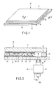
- FIG. 1 is a perspective view showing an FED according to a first embodiment of this invention;
- FIG. 2 is a sectional view of the FED taken along line II-II of FIG. 1;
- FIG. 3 is a sectional view showing an SIP in the FED;
- FIG. 4 is a sectional view schematically showing closed magnetic paths in the SIP;
- FIG. 5 is a sectional view showing a forming process for the SIP;
- FIG. 6 is a plan view showing the forming process for the SIP;
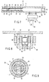
- FIG. 7 is a sectional view showing an FED according to a second embodiment of this invention;
- FIG. 8 is a sectional view showing the SIP of the second embodiment;
- FIG. 9 is a sectional view schematically showing closed magnetic paths in the SIP;
- FIG. 10 is a sectional view showing a forming process for the SIP; and
- FIG. 11 is a plan view showing the forming process for the SIP.
- An embodiment wherein an image display device with an SIP is applied to an FED will now be described in detail with reference to the drawings.
- As shown in FIGS. 1 and 2, the FED comprises a
front substrate 11 and arear substrate 12, which are formed of a rectangular glass sheet each. These substrates are opposed to each other across a gap of about 1 to 2 mm. Therear substrate 12 is formed larger than thefront substrate 11. Thefront substrate 11 and therear substrate 12 have their respective peripheral edge portions joined together by asidewall 18 in the form of a rectangular frame, and constitute a flat,rectangular vacuum envelope 10 that is kept in a vacuum inside. - A plurality of plate shaped
support members 14 are arranged in thevacuum envelope 10 in order to support atmospheric load that acts on thefront substrate 11 and therear substrate 12. Thesesupport members 14 individually extend parallel to one side of thevacuum envelope 10 and are arranged at given spaces along a direction perpendicular to the one side. Thesupport members 14 are not limited to the plate shape, and columnar ones may be used instead. - A
phosphor screen 16 that functions as an image display surface is formed on the inner surface of thefront substrate 11. Thephosphor screen 16 is formed by arranging red, green, and blue phosphor layers and a light absorbing layer situated between these phosphor layers. The phosphor layers extend parallel to the one side of thevacuum envelope 10 and are arranged at given spaces along a direction perpendicular to the one side. A metal back 17 of, e.g., aluminum and agetter film 15 are successively formed on thephosphor screen 16. - A large number of
electron emitting elements 22 are arranged on the inner surface of therear substrate 12. They serve as electron emitting sources that excite the phosphor layers of thephosphor screen 16. Theseelectron emitting elements 22 are arranged in a plurality of columns and a plurality of rows corresponding to individual pixels. More specifically, an electricallyconductive cathode layer 24 is formed on the inner surface of therear substrate 12, and asilicon dioxide film 26 having a large number ofcavities 25 are formed on the electrically conductive cathode layer.Gate electrodes 28 of molybdenum, niobium or the like are formed on thesilicon dioxide film 26. On the inner surface of therear substrate 12, the cone-shapedelectron emitting elements 22 of molybdenum or the like are provided in thecavities 25, individually. A large number ofwires 21 that supply potential to theelectron emitting elements 18 are provided in a matrix on the inner surface of thesecond substrate 12, and their end portions are drawn out to the peripheral edge portions of thevacuum envelope 15. - In the FED constructed in this manner, video signals are applied to the
electron emitting elements 22 and thegate electrodes 28 that are formed in a simple matrix. A gate voltage of +100V for example is applied to theelectron emitting elements 22 as a reference when in a highest-luminance state. Further, +10 kV for example is applied to thephosphor screen 16. Thereupon, electron beams are emitted from theelectron emitting elements 22. The electron beams emitted from theelectron emitting elements 22 are modulated in size by the voltage of thegate electrodes 28. These electron beams excite the phosphor layers of thephosphor screen 16 to luminescence, thereby displaying an image. - Since high voltage is applied to the
phosphor screen 16 in this manner, high-strain glass is used as plate glass for thefront substrate 11,rear substrate 12,sidewall 18, andsupport member 14. A space between therear substrate 12 and thesidewall 18 is sealed with low-meltingglass 19 such as fritted glass. A space between thefront substrate 11 and thesidewall 18 is sealed with asealing layer 21 that contains, for example, indium (In) as an electrically conductive low-melting sealing material. - In the
vacuum envelope 10, anexhaust port 40 is formed in an end portion of therear substrate 12. This exhaust port is connected with anSIP 50 that evacuates the interior of the vacuum envelope. TheSIP 50 has apump container 51 that is formed of a metal as a magnetic material; e.g., Fe/Ni alloy. Thepump container 51 is bonded to therear substrate 12 of thevacuum envelope 10 with frittedglass 42, communicates with the interior of the vacuum envelope through theexhaust port 40, and is kept with a vacuum inside. Thepump container 51 is not limited to the case where its entire body is formed of a magnetic material. Only a part of it may be formed of the magnetic material if it can form a closed magnetic path, as mentioned later. - As shown in FIGS. 2 to 4, a
cylindrical anode 53 is provided in the central part of the interior of thepump container 51. Plate-shapedcathodes 52 are located individually on the opposite opening sides of the anode and face the anode with given gaps between them. Eachcathode 52 is formed of titanium or tantalum, for example. A plate-shapedpermanent magnet 57 is provided between the inner surface of thepump container 51 and eachcathode 52. Thepermanent magnet 57 is in contact with the substantially entire surface of thecathode 52 as it is fixed to the cathode and the inner surface of the pump container. Thecathodes 52 are fixed to thepump container 51 by thepermanent magnets 57. A relatively negative voltage is applied from apower source 60 to thecathodes 52. - An
insulator 55 is attached to the lower end portion of thepump container 51, and anelectrode 56 is supported by theinsulator 55. Theelectrode 56 is drawn into thepump container 51 and connected to theanode 53. A relatively positive voltage is applied from thepower source 60 to theanode 53 through theelectrode 56. - According to the SIP constructed in this manner, a high voltage of 3 to 5 kV from the
power source 60 is applied between thecathodes 52 and theanode 53 in a manner such that a magnetic field perpendicular to thecathodes 52 is applied by thepermanent magnets 57 during operation. Thereupon, electrons are shot against gas molecules, ionizing released gas in thepump container 51. Gas plus ions generated by this ionization are shot against thecathodes 52 that are formed of, e.g., titanium plates, and use their energy to sputter titanium. Thereupon, an active titanium film is formed on the surface of theanode 53. Then, neutral molecules in the released gas and excited molecules land and adsorb on the titanium film and are exhausted. By this exhaust operation of theSIP 50, the released gas in thevacuum envelope 10 is discharged to keep the interior of the vacuum envelope at a high degree of vacuum of 10-5 Pa or below. - As shown in FIG. 4, the
pump container 51 of the magnetic material,cathodes 52, andpermanent magnets 57 form closedmagnetic paths 71, and the magnetic field generated by the permanent magnets passes through the closed magnetic paths without leaking to the outside. - The
SIP 50 constructed in this manner is manufactured by the following manufacturing method. As shown in FIGS. 5 and 6, theanode 53, thecathodes 52, and plate-shapedmagnetic members 54 fixed individually to the cathodes are first individually located in thepump container 51, and theinsulator 55 and theelectrode 56 are attached to the pump container. Subsequently, thepump container 51 is connected to thevacuum envelope 10, and the pump container is kept with a vacuum inside. Thereafter, a pair of magnetizingcoils 61 are located outside thepump container 51 and adjacently opposed to themagnetic members 54, individually. In this state, themagnetic members 54 are magnetized from outside thepump container 51 by the magnetizingcoils 61. Thereupon, themagnetic members 54 become thepermanent magnets 57 that generate amagnetic field 62 perpendicular to thecathodes 52. In these processes, theSIP 50 is formed connected to the vacuum envelope of the FED. - According to the SIP constructed in this manner, the
permanent magnets 57 are provided in thepump container 51 and located adjacent to thecathodes 52. Therefore, the opening distance of thepermanent magnets 57 can be made less than in the case where the permanent magnets are provided outside thepump container 51. Thus, the exhaust speed of theSIP 50 can be increased to maximize the exhaust efficiency. Further, thepermanent magnets 57 need not be provided outside thepump container 51, so that the pump can be miniaturized, and the assembly workability can be improved. - Since at least a part of the
pump container 51 is formed of the magnetic material, the pump container, permanent magnets, and cathodes can form the closed magnetic circuit to shield leaked magnetic fields. Thus, a great effect is produced when the SIP is used in combination with a device that is affected by leakage magnetism. - According to the SIP manufacturing method described above, a small-sized SIP can be easily formed by obtaining the permanent magnets by magnetizing the magnetic material, which is previously provided in the
pump container 51, from outside the pump container. - According to the FED, moreover, the interior of the
vacuum envelope 10 can be kept at a high degree of vacuum by theSIP 50, so that a stable display quality level can be maintained for a long time. - The following is a description of an FED according to a second embodiment of this invention. Like reference numerals are used to designate the same portions as those of the first embodiment, and a detailed description of them is omitted herein.
- As shown in FIGS. 7 to 9, a
rear substrate 12 of avacuum envelope 10 is provided with aSIP 50 that discharges released gas from thevacuum envelope 10. TheSIP 50 has apump container 51 that is formed of a nonmetal, e.g., glass. In the present embodiment, thepump container 51 is bonded to therear substrate 12 of glass with frittedglass 40, internally communicates with the interior of the vacuum envelope, and is kept with a vacuum inside. - A pair of
cathodes 52 and ananode 53 are located in thepump container 51. Thecathodes 52 are formed by bending metal plates of titanium or tantalum into a substantially U-shaped profile and are opposed to each other with a given space between them. Thesecathodes 52 are individually fixed to thepump container 51 by anonpenetrating terminal 75 and a penetratingterminal 76. Theanode 53 is located between the pair ofcathodes 52 and opposed to thecathodes 52 with given gaps between them. Theanode 53 is supported in thepump container 51 by anelectrode 56. A relatively negative voltage and a relatively positive voltage are applied from apower source 60 outside thevacuum envelope 10 to thecathodes 52 and theanode 53 through the penetratingterminal 76 and theelectrode 56, respectively. - A pair of
permanent magnets 57 are provided in thepump container 51 and individually located between the inner surface of thepump container 51 and thecathodes 52. Eachpermanent magnet 57 is in contact with the substantially entire surface of thecathode 52 as it is fixed to the cathode. A magnetic body in the shape of a closed loop, e.g., an annularmagnetic body 66, is mounted outside thepump container 51 and faces thepermanent magnets 57. Themagnetic body 66, along with thecathodes 52 and thepermanent magnets 57, forms closedmagnetic paths 71. - According to the SIP constructed in this manner, a high voltage of 3 to 5 kV from the
power source 60 is applied between thecathodes 52 and theanode 53 in a manner such that a magnetic field perpendicular to thecathodes 52 is applied by thepermanent magnets 57 during operation. Thereupon, electrons are shot against gas molecules, ionizing released gas in thepump container 51. Gas plus ions generated by this ionization are shot against thecathodes 52 that are formed of, e.g., titanium plates, and use their energy to sputter titanium. Thereupon, an active titanium film is formed on the surface of theanode 53. Then, neutral molecules in the released gas and excited molecules land and adsorb on the titanium film and are exhausted. By this exhaust operation of theSIP 50, the released gas in thevacuum envelope 10 is discharged to keep the interior of the vacuum envelope at a high degree of vacuum of 10-5 Pa or below. - As shown in FIG. 9, the
magnetic body 66,cathodes 52, andpermanent magnets 57 form the closedmagnetic paths 71, and the magnetic field generated by the permanent magnets passes through the closed magnetic paths without leaking to the outside. - The
SIP 50 constructed in this manner is manufactured by the following manufacturing method. As shown in FIGS. 10 and 11, thepump container 51, in which theanode 53; thecathodes 52, and themagnetic members 54 fixed to thecathodes 52 are arranged, is first bonded to therear substrate 12 with the frittedglass 40. - Subsequently, the
rear substrate 12,front substrate 11, andsidewall 18 are assembled to form thevacuum envelope 10 with a vacuum inside. At the same time, thepump container 51 is evacuated. Thereafter, a pair of magnetizingcoils 61 are located outside thepump container 51 and adjacently opposed to themagnetic members 54, individually. In this state, the magnetizing coils 61 apply an electric field to themagnetic members 54 to magnetize them from outside thepump container 51. Thereupon, themagnetic members 54 become thepermanent magnets 57 that generate amagnetic field 65 perpendicular to thecathodes 52. Thereafter, the annularmagnetic body 66 is mounted outside thepump container 51. In these processes, theSIP 50 is formed connected to the vacuum envelope of the FED. - According to the
SIP 50 constructed in this manner, thepermanent magnets 57 are provided in thepump container 51 and located adjacent to thecathodes 52. Therefore, the opening distance of thepermanent magnets 57 can be made less than in the case where the permanent magnets are provided outside thepump container 51. Thus, the exhaust speed of theSIP 50 can be increased to maximize the exhaust efficiency. Thepermanent magnets 57 need not be provided outside thepump container 51, so that the pump can be miniaturized, and the assembly workability can be improved. - The magnetic body in the shape of a closed loop is provided outside the
pump container 51, and forms the closedmagnetic paths 71 in cooperation with thepermanent magnets 57 and thecathodes 52, so that leaked magnetic fields can be shielded. Thus, a great effect is produced when theSIP 50 is used in combination with a device that is affected by leakage magnetism. - According to the SIP manufacturing method described above, a small SIP can be easily formed by obtaining the permanent magnets by magnetizing the magnetic material, which is previously provided in the
pump container 51, from outside the pump container. - According to the FED, moreover, the interior of the
vacuum envelope 10 can be kept at a high degree of vacuum by theSIP 50, so that a stable display quality level can be maintained for a long time. As this is done, the assemblability can be improved and the entire device can be miniaturized by using a part of thevacuum envelope 10 to form thepump container 51 of theSIP 50, e.g., by molding the pump container integrally with the rear substrate. - The present invention is not limited to the embodiments described above, and various modifications may be effected therein without departing from the scope of the invention. Further, the foregoing embodiments include inventions of various stages, and various inventions can be extracted by appropriately combining a plurality of disclosed required constituent elements. For example, if the problem described in the paragraph titled "Problem to be solved by the Invention" can be solved despite elimination of any of all the required constituent elements according to the embodiments, and if the effect described in the paragraph titled "Effect of the Invention" can be obtained, configurations from which the required constituent elements are eliminated can be extracted as inventions.
- In the foregoing embodiments, the pump container is formed of a dedicated container for an SIP that is provided with an electrode outlet portion. Alternatively, for example, a part of a metallic vacuum envelope may be formed of a magnetic material to form a pump container of an SIP. Also in this case, the same function and effect as those of the foregoing embodiments can be obtained. In the foregoing embodiments, moreover, the magnetic body is provided to form the closed magnetic paths. Even if this magnetic body is omitted, however, the SIP with high exhaust efficiency can be obtained. The shapes, materials, etc., of the components of the SIP are not limited to those of the foregoing embodiments but may be variously selected as required.
- Although the electron emitting elements used are of the field-emission type, they may alternatively be replaced with any other electron emitting elements, such as pn-type cold-cathode devices or surface-conduction electron emitting elements.
- According to the SIP constructed in this manner, there may be provided a sputter ion pump which, comprising permanent magnets located adjacent to cathodes in a pump container, is small and has high exhaust efficiency and improved magnetic field shielding properties, a manufacturing method therefor, and an image display device provided with the sputter ion pump and capable of maintaining a stable display quality level for a long time.
Claims (17)
- A sputter ion pump comprising:a pump container;a cathode and an anode opposed to each other in the pump container; anda permanent magnet located in the pump container and situated between the cathode and the inner surface of the pump container.
- The sputter ion pump according to claim 1, wherein the permanent magnet is in contact with or fixed to the cathode.
- The sputter ion pump according to claim 1 or 2, wherein the pump container is formed of a metal.
- The sputter ion pump according to claim 3, wherein at least a part of the pump container is formed of a magnetic material.
- The sputter ion pump according to claim 1 or 2, wherein the pump container is formed of a nonmetal.
- The sputter ion pump according to claim 5, wherein the pump container is formed of glass.
- The sputter ion pump according to claim 5, wherein a magnetic body in the shape of a closed loop which defines a closed magnetic path is provided outside the pump container so as to face the permanent magnet.
- A method of manufacturing a sputter ion pump which comprises a pump container, a cathode and an anode opposed to each other in the pump container, and a permanent magnet located in the pump container and situated between the cathode and the inner surface of the pump container, the manufacturing method of a sputter ion pump comprising:locating the anode, cathode, and magnetic material in the pump container and then magnetizing the magnetic material from outside the pump container, thereby forming the permanent magnet.
- The manufacturing method for a sputter ion pump according to claim 8, wherein the magnetic material is magnetized with the pump container evacuated inside.
- An image display device comprising:a vacuum envelope which includes a front substrate having a phosphor screen and a rear substrate provided with a plurality of electron emission sources which excite the phosphor screen and is kept with a vacuum inside; anda sputter ion pump connected to the vacuum envelope and configured to exhaust the vacuum envelope,the sputter ion pump comprising a pump container connected to the vacuum envelope and having a vacuum inside, a cathode and an anode opposed to each other in the pump container, and a permanent magnet located in the pump container and situated between the cathode and the inner surface of the pump container.
- The image display device according to claim 10, wherein the permanent magnet is in contact with or fixed to the cathode.
- The image display device according to claim 11 or 12, wherein the pump container is formed of a metal.
- The image display device according to claim 12, wherein at least a part of the pump container is formed of a magnetic material.
- The image display device according to claim 11 or 12, wherein the pump container is formed of a nonmetal.
- The image display device according to claim 14, wherein the pump container is formed of glass.
- The image display device according to claim 14, wherein a magnetic body in the shape of a closed loop which forms a closed magnetic path is provided outside the pump container so as to face the permanent magnet.
- The image display device according to claim 11 or 12, wherein the pump container is formed by molding a part of the rear substrate.
Applications Claiming Priority (3)
| Application Number | Priority Date | Filing Date | Title |
|---|---|---|---|
| JP2003142240A JP3927147B2 (en) | 2003-05-20 | 2003-05-20 | Manufacturing method of sputter ion pump |
| JP2003142241A JP3920811B2 (en) | 2003-05-20 | 2003-05-20 | Manufacturing method of sputter ion pump |
| PCT/JP2004/007062 WO2004105080A1 (en) | 2003-05-20 | 2004-05-18 | Sputter ion pump, process for manufacturing the same, and image display with sputter ion pump |
Publications (2)
| Publication Number | Publication Date |
|---|---|
| EP1626434A1 true EP1626434A1 (en) | 2006-02-15 |
| EP1626434A4 EP1626434A4 (en) | 2006-12-20 |
Family
ID=33478954
Family Applications (1)
| Application Number | Title | Priority Date | Filing Date |
|---|---|---|---|
| EP04733679A Withdrawn EP1626434A4 (en) | 2003-05-20 | 2004-05-18 | Sputter ion pump, process for manufacturing the same, and image display with sputter ion pump |
Country Status (5)
| Country | Link |
|---|---|
| US (1) | US20060078433A1 (en) |
| EP (1) | EP1626434A4 (en) |
| KR (1) | KR20060013545A (en) |
| TW (1) | TWI269337B (en) |
| WO (1) | WO2004105080A1 (en) |
Cited By (1)
| Publication number | Priority date | Publication date | Assignee | Title |
|---|---|---|---|---|
| WO2024089575A1 (en) * | 2022-10-27 | 2024-05-02 | Edwards Vacuum Llc | Sputter ion pump |
Families Citing this family (5)
| Publication number | Priority date | Publication date | Assignee | Title |
|---|---|---|---|---|
| JP2006066265A (en) * | 2004-08-27 | 2006-03-09 | Canon Inc | Image display device |
| EP2249373B1 (en) * | 2008-02-14 | 2017-08-02 | National Institute of Information and Communications Technology | Ion pump system and electromagnetic field generator |
| KR101134308B1 (en) * | 2009-06-01 | 2012-04-16 | 주식회사 브이엠티 | Ion pump with surface treated permanent magnet |
| ES2734456T3 (en) | 2013-09-19 | 2019-12-10 | Fuchs Petrolub Se | Inorganic functional layer on hot dipped galvanized steel to aid shaping |
| US9960026B1 (en) * | 2013-11-11 | 2018-05-01 | Coldquanta Inc. | Ion pump with direct molecule flow channel through anode |
Family Cites Families (12)
| Publication number | Priority date | Publication date | Assignee | Title |
|---|---|---|---|---|
| US3107045A (en) * | 1961-02-02 | 1963-10-15 | Varian Associates | Getter ion pump apparatus |
| JPS5065359U (en) * | 1973-10-15 | 1975-06-12 | ||
| JPS50105358U (en) * | 1974-02-05 | 1975-08-29 | ||
| IT1156530B (en) * | 1982-09-14 | 1987-02-04 | Varian Spa | IONIC PUMP WITH CATHODE PERFECTLY STRUCTURE PARTICULARLY FOR PUMPING NOBLE GASES |
| JPS6351037A (en) * | 1986-08-20 | 1988-03-04 | Toshiba Corp | Anode chamber of electron beam device |
| JPH05121012A (en) * | 1991-10-29 | 1993-05-18 | Sony Corp | Thin type plane display device |
| JP3492772B2 (en) * | 1993-09-20 | 2004-02-03 | 株式会社東芝 | X-ray image intensifier |
| JP3325982B2 (en) * | 1993-12-27 | 2002-09-17 | 株式会社東芝 | Magnetic field immersion type electron gun |
| JPH0822803A (en) * | 1994-07-08 | 1996-01-23 | Ulvac Japan Ltd | Sputter ion pump |
| JPH09213261A (en) * | 1996-02-01 | 1997-08-15 | Hamamatsu Photonics Kk | Ion pump |
| JP3666976B2 (en) * | 1996-03-13 | 2005-06-29 | キヤノン株式会社 | Image display device |
| IT1307236B1 (en) * | 1999-04-02 | 2001-10-30 | Varian Spa | IONIC PUMP. |
-
2004
- 2004-05-18 KR KR1020057021975A patent/KR20060013545A/en not_active Abandoned
- 2004-05-18 EP EP04733679A patent/EP1626434A4/en not_active Withdrawn
- 2004-05-18 WO PCT/JP2004/007062 patent/WO2004105080A1/en not_active Ceased
- 2004-05-20 TW TW093114322A patent/TWI269337B/en not_active IP Right Cessation
-
2005
- 2005-11-18 US US11/281,374 patent/US20060078433A1/en not_active Abandoned
Cited By (1)
| Publication number | Priority date | Publication date | Assignee | Title |
|---|---|---|---|---|
| WO2024089575A1 (en) * | 2022-10-27 | 2024-05-02 | Edwards Vacuum Llc | Sputter ion pump |
Also Published As
| Publication number | Publication date |
|---|---|
| TWI269337B (en) | 2006-12-21 |
| TW200426875A (en) | 2004-12-01 |
| EP1626434A4 (en) | 2006-12-20 |
| US20060078433A1 (en) | 2006-04-13 |
| WO2004105080A1 (en) | 2004-12-02 |
| KR20060013545A (en) | 2006-02-10 |
Similar Documents
| Publication | Publication Date | Title |
|---|---|---|
| US20060078433A1 (en) | Sputter ion pump and manufacturing method therefor and image display device with sputter ion pump | |
| US7385344B2 (en) | Electron emission device including dummy electrodes | |
| US5717292A (en) | Plasma displays employing magnetic enhancement | |
| US6670753B1 (en) | Flat panel display with gettering material having potential of base, gate or focus plate | |
| US7129630B2 (en) | Display device | |
| US7319286B2 (en) | Display device | |
| JP3927147B2 (en) | Manufacturing method of sputter ion pump | |
| JP2006066273A (en) | Image display device | |
| JP3920811B2 (en) | Manufacturing method of sputter ion pump | |
| US6743068B2 (en) | Desorption processing for flat panel display | |
| KR0183548B1 (en) | Field emission indicator | |
| JP2005302377A (en) | Sputter ion pump and image display device provided with sputter ion pump | |
| JP2006066211A (en) | Sputter ion pump and image display device | |
| JP2006066293A (en) | Sputter ion pump and image display device | |
| US20070120460A1 (en) | Image display device | |
| KR100511266B1 (en) | Spacerless field emission device | |
| JP2005293921A (en) | Sputter ion pump and image display device provided with sputter ion pump | |
| JP2006093026A (en) | Sputter ion pump and image display device | |
| KR0160007B1 (en) | Field emission display | |
| JP2004071294A (en) | Image display device and method of manufacturing the same | |
| JP2006073414A (en) | Image display device | |
| JP2006012531A (en) | Flat panel display | |
| JP2007066894A (en) | Anode element and field emission display using the anode element | |
| KR101009978B1 (en) | Field emission display device and manufacturing method thereof | |
| JP2003031166A (en) | Image display device |
Legal Events
| Date | Code | Title | Description |
|---|---|---|---|
| PUAI | Public reference made under article 153(3) epc to a published international application that has entered the european phase |
Free format text: ORIGINAL CODE: 0009012 |
|
| 17P | Request for examination filed |
Effective date: 20051118 |
|
| AK | Designated contracting states |
Kind code of ref document: A1 Designated state(s): DE FR GB IT NL |
|
| RIN1 | Information on inventor provided before grant (corrected) |
Inventor name: SEINO, KAZUYUKI C/O INTEL.PRO. DIV. TOSHIBA CORP Inventor name: SHIMADA, YOSHIYUKIC/O INT. PRO. DIV. TOSHIBA CORP |
|
| RIN1 | Information on inventor provided before grant (corrected) |
Inventor name: SHIMADA, YOSHIYUKIC/O INT. PRO. DIV. TOSHIBA CORP Inventor name: SEINO, KAZUYUKI C/O INTEL.PRO. DIV. TOSHIBA CORP |
|
| DAX | Request for extension of the european patent (deleted) | ||
| RBV | Designated contracting states (corrected) |
Designated state(s): DE FR GB IT NL |
|
| A4 | Supplementary search report drawn up and despatched |
Effective date: 20061116 |
|
| 17Q | First examination report despatched |
Effective date: 20071106 |
|
| STAA | Information on the status of an ep patent application or granted ep patent |
Free format text: STATUS: THE APPLICATION IS DEEMED TO BE WITHDRAWN |
|
| 18D | Application deemed to be withdrawn |
Effective date: 20080318 |