EP1626411A1 - Shared address lines for crosspoint memory - Google Patents
Shared address lines for crosspoint memory Download PDFInfo
- Publication number
- EP1626411A1 EP1626411A1 EP04425631A EP04425631A EP1626411A1 EP 1626411 A1 EP1626411 A1 EP 1626411A1 EP 04425631 A EP04425631 A EP 04425631A EP 04425631 A EP04425631 A EP 04425631A EP 1626411 A1 EP1626411 A1 EP 1626411A1
- Authority
- EP
- European Patent Office
- Prior art keywords
- memory
- cell
- voltage
- address line
- biasing
- Prior art date
- Legal status (The legal status is an assumption and is not a legal conclusion. Google has not performed a legal analysis and makes no representation as to the accuracy of the status listed.)
- Withdrawn
Links
- 230000015654 memory Effects 0.000 title claims abstract description 119
- 239000000463 material Substances 0.000 claims description 64
- 238000000034 method Methods 0.000 claims description 21
- 230000008859 change Effects 0.000 claims description 14
- 150000004770 chalcogenides Chemical class 0.000 claims description 10
- 238000004519 manufacturing process Methods 0.000 abstract description 2
- 239000012782 phase change material Substances 0.000 description 7
- 238000010438 heat treatment Methods 0.000 description 5
- 239000002184 metal Substances 0.000 description 5
- 238000001816 cooling Methods 0.000 description 3
- 230000003071 parasitic effect Effects 0.000 description 3
- 230000008569 process Effects 0.000 description 3
- 230000004044 response Effects 0.000 description 3
- 239000004065 semiconductor Substances 0.000 description 3
- 230000008901 benefit Effects 0.000 description 2
- 238000012986 modification Methods 0.000 description 2
- 230000004048 modification Effects 0.000 description 2
- -1 silicon oxide nitride Chemical class 0.000 description 2
- 229910000618 GeSbTe Inorganic materials 0.000 description 1
- BUGBHKTXTAQXES-UHFFFAOYSA-N Selenium Chemical compound [Se] BUGBHKTXTAQXES-UHFFFAOYSA-N 0.000 description 1
- NINIDFKCEFEMDL-UHFFFAOYSA-N Sulfur Chemical compound [S] NINIDFKCEFEMDL-UHFFFAOYSA-N 0.000 description 1
- 239000000956 alloy Substances 0.000 description 1
- 229910045601 alloy Inorganic materials 0.000 description 1
- 229910052787 antimony Inorganic materials 0.000 description 1
- 230000001413 cellular effect Effects 0.000 description 1
- 229910052798 chalcogen Inorganic materials 0.000 description 1
- 150000001787 chalcogens Chemical class 0.000 description 1
- 238000004891 communication Methods 0.000 description 1
- 238000002425 crystallisation Methods 0.000 description 1
- 230000008025 crystallization Effects 0.000 description 1
- 238000013500 data storage Methods 0.000 description 1
- 230000001419 dependent effect Effects 0.000 description 1
- 238000013461 design Methods 0.000 description 1
- 239000007772 electrode material Substances 0.000 description 1
- 230000005669 field effect Effects 0.000 description 1
- 230000006870 function Effects 0.000 description 1
- 230000005055 memory storage Effects 0.000 description 1
- 229910044991 metal oxide Inorganic materials 0.000 description 1
- 150000004706 metal oxides Chemical class 0.000 description 1
- 238000001465 metallisation Methods 0.000 description 1
- 239000000203 mixture Substances 0.000 description 1
- 230000000737 periodic effect Effects 0.000 description 1
- 229920000642 polymer Polymers 0.000 description 1
- 238000012545 processing Methods 0.000 description 1
- 230000000717 retained effect Effects 0.000 description 1
- 229910052711 selenium Inorganic materials 0.000 description 1
- 239000011669 selenium Substances 0.000 description 1
- 229910052814 silicon oxide Inorganic materials 0.000 description 1
- 238000001228 spectrum Methods 0.000 description 1
- 230000003068 static effect Effects 0.000 description 1
- 229910052717 sulfur Inorganic materials 0.000 description 1
- 239000011593 sulfur Substances 0.000 description 1
- 229910052714 tellurium Inorganic materials 0.000 description 1
- PORWMNRCUJJQNO-UHFFFAOYSA-N tellurium atom Chemical compound [Te] PORWMNRCUJJQNO-UHFFFAOYSA-N 0.000 description 1
Images




Classifications
-
- G—PHYSICS
- G11—INFORMATION STORAGE
- G11C—STATIC STORES
- G11C11/00—Digital stores characterised by the use of particular electric or magnetic storage elements; Storage elements therefor
- G11C11/21—Digital stores characterised by the use of particular electric or magnetic storage elements; Storage elements therefor using electric elements
- G11C11/22—Digital stores characterised by the use of particular electric or magnetic storage elements; Storage elements therefor using electric elements using ferroelectric elements
-
- G—PHYSICS
- G11—INFORMATION STORAGE
- G11C—STATIC STORES
- G11C11/00—Digital stores characterised by the use of particular electric or magnetic storage elements; Storage elements therefor
- G11C11/02—Digital stores characterised by the use of particular electric or magnetic storage elements; Storage elements therefor using magnetic elements
- G11C11/16—Digital stores characterised by the use of particular electric or magnetic storage elements; Storage elements therefor using magnetic elements using elements in which the storage effect is based on magnetic spin effect
-
- G—PHYSICS
- G11—INFORMATION STORAGE
- G11C—STATIC STORES
- G11C13/00—Digital stores characterised by the use of storage elements not covered by groups G11C11/00, G11C23/00, or G11C25/00
- G11C13/0002—Digital stores characterised by the use of storage elements not covered by groups G11C11/00, G11C23/00, or G11C25/00 using resistive RAM [RRAM] elements
- G11C13/0004—Digital stores characterised by the use of storage elements not covered by groups G11C11/00, G11C23/00, or G11C25/00 using resistive RAM [RRAM] elements comprising amorphous/crystalline phase transition cells
-
- G—PHYSICS
- G11—INFORMATION STORAGE
- G11C—STATIC STORES
- G11C5/00—Details of stores covered by group G11C11/00
- G11C5/06—Arrangements for interconnecting storage elements electrically, e.g. by wiring
- G11C5/063—Voltage and signal distribution in integrated semi-conductor memory access lines, e.g. word-line, bit-line, cross-over resistance, propagation delay
-
- G—PHYSICS
- G11—INFORMATION STORAGE
- G11C—STATIC STORES
- G11C2213/00—Indexing scheme relating to G11C13/00 for features not covered by this group
- G11C2213/70—Resistive array aspects
- G11C2213/79—Array wherein the access device being a transistor
Definitions
- This invention relates generally to crosspoint memories.
- Crosspoint memories are memories that use transverse addressing lines, such as row and column lines, with intervening programmable material.
- Examples of crosspoint memories include magnetic tunnel junction memory, resistive random access memory, ferroelectric random access memory, silicon oxide nitride oxide semiconductor memory, polymer memory, and phase change memory.
- Phase change memory devices use phase change materials, i.e., materials that may be electrically switched between a generally amorphous and a generally crystalline state, as an electronic memory.
- phase change materials i.e., materials that may be electrically switched between a generally amorphous and a generally crystalline state
- One type of memory element utilizes a phase change material that may be, in one application, electrically switched between generally amorphous and generally crystalline local orders or between different detectable states of local order across the entire spectrum between completely amorphous and completely crystalline states.
- Typical materials suitable for such an application include various chalcogenide elements.
- the state of the phase change materials is also non-volatile.
- the memory When the memory is set in either a crystalline, semi-crystalline, amorphous, or semi-amorphous state representing a resistance value, that value is retained until reprogrammed, even if power is removed. This is because the programmed value represents a phase or physical state of the material (e.g., crystalline or amorphous).
- a biasing method a method for forming a cross-point memory, a cross-point memory and a system, as defined respectively in claims 1, 12, 16 and 23.
- a crosspoint memory 10 in accordance with one embodiment of the present invention, may be implemented as a phase change memory.
- the memory 10 may include address lines 12a and 12c extending in a first direction and generally transverse address lines 12b and 12d. Of course, a large number of additional lines may be provided.
- pairs of adjacent transverse lines 12 define at least one cell between them including a phase change memory element 14 and a chalcogenide selection device 16.
- a selection device 16 between the lines 12, turns on, allowing current flow across a memory element 14.
- crosspoint memory implemented as a phase change memory
- any other crosspoint memory may be used in other embodiments of the present invention.
- phase change memory element 14 may be implemented by a series of layers provided underneath the selection device 16 in one embodiment. Vias 18 may be provided between adjacent, but transverse lines 12, such as the lines 12a and 12b.
- lines 12 such as the line 12d1
- lines 12d is shared between an overlying cell (including the element 14d and the selection device 16d) and an underlying cell (including the selection device 16c and the memory element 14c).
- the line 12c functions for selection of the overlying cell (including the selection device 16c and the memory element 14c), as well as for selection of the memory element 14b and selection device 16b underlying the line 12c.
- a voltage biasing system is used.
- a read or write voltage V is applied.
- a supply voltage V may be applied to the line 12c.
- the selected column includes a cell made up of the selection device 16b and the memory element 14b. The selection is achieved by providing a zero voltage on the appropriate line 12b, labeled line 'B' in Figure 3, and a read or write voltage V on the line 12c in this embodiment.
- unselected columns such as the lines 12d or 12b, may be biased at half the read or write voltage V (i.e., one-half V).
- the line 12a may also be at half the read or write voltage V (i.e., one-half V).
- the potential across the cells between unselected columns and unselected rows is zero.
- parasitic current may be significantly reduced.
- the cell made up of the selection device 16b and memory element 14b has a half voltage bias across it in one embodiment.
- the cells between the selected column and unselected rows have half voltage across them.
- the cells between the selected row and unselected columns have half voltage across them. But the half voltage may be such that it is insufficient to turn on the selection device 16b.
- parasitic currents can be reduced in unselected columns and read or write disturbs in unselected cells may also be reduced.
- the unselected row lines and unselected column lines are held at the half voltage potential.
- the selected row line is at zero volts or ground and the selected column line is ramped to the required voltage V for the intended read or write operation. If the maximum column voltage on the selected column line is ramped to the voltage V, which may be up to the supply voltage, then the maximum voltage across an unselected element, such as an element 14 in series with the selection device 16, is half the voltage V. Sharing row and column metallizations may reduce the processing steps needed for each plane of memory in one embodiment.
- the elements 14 and devices 16 are in the same polarity or orientation, such that the selection device 16 is fabricated after the memory element 14 so that the selection device 16 is on top.
- the read or write pulse comes in on top and the bottom line of the selected cell is held at ground.
- the current sources for reading and writing may be able to force current on columns or rows.
- the current for reading and writing flows in the same direction from top to bottom for the select device and memory element. If the bottom conductive line is at ground and the top conductive line is at a positive voltage V, then current flows in a positive direction from top to bottom. If either the select device or memory device has asymmetrical iv characteristics then this method of operation would be desirable. Also it permits the same fabrication sequence (e.g. memory device on bottom (first) followed by the select device on top (last) to be utilized for all the elements).
- the selection devices 16 may be designed, in one embodiment, such that the level of voltage across the unselected cells only results in minimal parasitic leakage current and, thus, does not impact either the read or the write to the selected memory device while avoiding any disturb of unselected bits.
- the voltage utilized for reading a selected memory bit may be less and, thus, there may be a wider design window for the selection device 16 to avoid significant conduction during the read operation.
- the voltage required to write the memory element 14 may be higher and, thus, there is more of a concern of leakage to the unselected bits during the write operation. To give more margin, it may be desirable to bias the memory for read and write operations at one-third the supply voltage or to bias at one-half for reading and one-third for writing in some embodiments.
- the material 64 in Figure 2, may be a phase change material suitable for non-volatile memory data storage.
- the phase change material may be a material having electrical properties (e.g., resistance) that may be changed through the application of energy such as, for example, heat, light, voltage potential, or electrical current.
- phase change materials may include a chalcogenide material or an ovonic material.
- An ovonic material may be a material that undergoes electronic or structural changes in response to an application of a voltage potential, electrical current, light, heat, etc.
- a chalcogenide material may be a material that includes at least one element from column VI of the periodic table or may be a material that includes one or more of the chalcogen elements, e.g., any of the elements of tellurium, sulfur, or selenium.
- Ovonic and chalcogenide materials may be non-volatile memory materials that may be used to store information.
- the memory material 64 may be chalcogenide element composition from the class of tellurium-germanium-antimony (Te x Ge y Sb z ) material or a GeSbTe alloy, although the scope of the present invention is not limited to just these materials.
- the memory material 64 may be programmed into one of at least two memory states by applying an electrical signal to the memory material.
- An electrical signal may alter the phase of the memory material between a substantially crystalline state and a substantially amorphous state, wherein the electrical resistance of the memory material 64 in the substantially amorphous state is greater than the resistance of the memory material in the substantially crystalline state.
- the memory material 64 may be adapted to be altered to a particular one of a number of resistance values within a range of resistance values to provide digital or analog storage of information.
- Programming of the memory material to alter the state or phase of the material may be accomplished by applying voltage potentials to the adjacent lines 12, thereby generating a voltage potential across the memory material 64.
- An electrical current may flow through a portion of the memory material 64 in response to the applied voltage potentials, and may result in heating of the memory material 64.
- This controlled heating and subsequent controlled cooling may alter the memory state or phase of the memory material 64. Altering the phase or state of the memory material 64 may alter an electrical characteristic of the memory material 64. For example, resistance of the material 64 may be altered by altering the phase of the memory material 64. Either all or a portion of the phase change memory material may be altered during the writing pulse (i.e. only a portion/region of element 64 adjacent to either the top or bottom electrode may be phase changed during the write operation. In one embodiment primarily the portion of layer 64 that under goes phase change is the region that is adjacent to the smaller lower electrode.
- the memory material 64 may also be referred to as a programmable resistive material or simply a programmable resistance material.
- a voltage pulse with a potential difference of about 0.5 to 1.5 V may be applied across a portion of the memory material by applying about 0 volts to a lower line 12 and about 0.5 to 1.5 V to an upper line 12.
- a current flowing through the memory material 64 in response to the applied voltage potentials may result in heating of the memory material. This heating and subsequent cooling may alter the memory state or phase of the material.
- the memory material In a "reset" state, the memory material may be in an amorphous or semi-amorphous state and in a "set” state, the memory material may be in a crystalline or semi-crystalline state.
- the resistance of the memory material in the amorphous or semi-amorphous state may be greater than the resistance of the material in the crystalline or semi-crystalline state.
- the memory material 64 may be heated to a relatively higher temperature and then subsequently cooled at a fast rate to amorphisize memory material and "reset" memory material. Heating the volume or memory material to a relatively lower crystallization temperature may crystallize memory material and "set” memory material.
- Various resistances of memory material may be achieved to store information by varying the amount of current flow and duration through the volume of memory material, or by tailoring the edge rate of the trailing edge of the programming current or voltage pulse (that may impact the cooling rate of the select memory element).
- the information stored in memory material 64 may be read by measuring the resistance of the memory material.
- a read current may be provided to the memory material using opposed lines 12 and a resulting read voltage across the memory material may be compared against a reference voltage using, for example, the sense amplifier (not shown).
- the read voltage may be proportional to the resistance exhibited by the memory storage element.
- the device 16 is off and may exhibit very high resistance in some embodiments.
- the off resistance can, for example, range from 50,000 ohms to greater than 10 gigaohms at a bias of half the threshold voltage.
- the device 16 may remain in its off state until a threshold voltage V T or threshold current IT switches the device 16 to a highly conductive, low resistance on state.
- the voltage across the device 16 after turn on drops to a slightly lower voltage, called the holding voltage v H and remains very close to this holding voltage.
- the threshold voltage may be on the order of 1.1 volts and the holding voltage may be on the order of .9 volts.
- the device 16 voltage drop remains close to the holding voltage as the current passing through the device is increased up to a certain, relatively high, current level. Above that current level the device remains on but displays a finite differential resistance with the voltage drop increasing with increasing current.
- the device 16 may remain on until the current through the device 16 is dropped below a characteristic holding current value that is dependent on the area of the material and may be impacted by the top and bottom electrodes utilized to form the device 16.
- the selection device 16 does not change phase. It remains permanently amorphous and its current-voltage characteristics may remain the same throughout its operating life.
- the holding current may be on the order of 0.1 to 100 micro-amps ( ⁇ A) in one embodiment. Below this holding current, the device 16 turns off and returns to the high resistance regime at low voltage, low field.
- the threshold current for the device 16 may generally be of the same order as the holding current.
- the holding current may be altered by changing process variables, such as the top and bottom electrode material and the chalcogenide material.
- the device 16 may provide high "on current" for a given area of device compared to conventional access devices such as metal oxide semiconductor field effect transistors or bipolar junction transistors or semiconductor diodes.
- the higher current density of the device 16 in the on state allows for higher programming current available to the memory element 14.
- the memory element 14 is a phase change memory
- this enables the use of larger programming current phase change memory devices, potentially reducing the need for sub-lithographic feature structures and the commensurate process complexity, cost, process variation, and device parameter variation.
- the read/write current may be forced in either direction.
- the voltage for reading or writing is forced into the page along the line 12 (labeled "METAL N+1 LINE B,") which is transverse to direction current was forced on the line 12c in the embodiment of Figure 3.
- reading or writing may be done from the "bottom up".
- the addressing line 12a is supplied with the read or write voltage and the cell including the memory element 14a and the selection device 16a has a voltage difference sufficient to turn on the selection device 16a.
- the read or write voltage is placed on the line 12a
- zero volts may be placed on the line 12b (labeled "METAL N+1 LINE B").
- reading or writing is possible from the top down ( Figure 4) or the bottom up ( Figure 5), depending on which plane of the memory is being accessed.
- One advantage of the embodiment of Figure 5, compared to the embodiment of Figure 4, is that it is not necessary in the embodiment of Figure 5 to have current sources for reading or writing that are able to force current in the direction into the page.
- Figure 6 shows another embodiment of the present invention in which different bias voltages are utilized.
- the supply voltage divided by three may be utilized for biasing.
- the advantage of the one-third supply voltage biasing scheme in one embodiment for a single plane of memory may include increased voltage margin, since the maximum voltage across the unselected bits is now reduced to the supply voltage divided by three rather than the supply voltage divided by two.
- One disadvantage in some embodiments of the one-third supply voltage biasing scheme may be increased current between the unselected rows and unselected columns, since those rows and columns now have a voltage potential across them of one-third the supply voltage compared to no voltage across them per the half supply voltage bias scheme.
- the read/write voltage is applied to the line 12c and zero volts are applied to the line 12b (labeled "METAL N+1 LINE B") in one embodiment.
- the selection device 16b turns on, and the memory element 14b can be read or written to.
- the unselected lines may have a voltage of two-thirds or one third of the read/write voltage applied to them.
- a voltage difference of one-third the supply voltage is applied across the cell (V-2/3V).
- Figure 7 corresponds to Figure 6 except now the unselected lines 12b receive one-third the voltage V, and the lower selected line 12a receives a voltage of zero in this embodiment.
- the unselected cells between the unselected Metal N+1 and the Metal N have (R-1)* C-1)cells in parallel with V/3 voltage across them.
- the unselected cells between the unselected Metal N+1 and Metal N+2 have (R-1) * (C-1) cells in parallel with V/3 voltage across them leading to standby current (where R is the number of rows and C is the number of columns).
- BL may correspond to a selected line 12a or 12b or 12c
- WL may correspond to a selected line 12b or 12c or 12d (note: the BL is upper line and the WL is typically the lower line from Figures 1, 3).
- Vcc/2 100 ⁇ A-1mA Vcc/2 Vcc/2 0 V Vcc/2 Vcc/2 SET Vcc/2 50 ⁇ A-650 ⁇ A Vcc/2 Vcc/2 0 V Vcc/2 Vcc/2 READ Vcc/2 5 ⁇ A 0 100 ⁇ A Vcc/2 Vcc/2 0 V Vcc/2 Vcc/2
- the table below shows a corresponding arrangement for one embodiment of the one-third supply voltage biasing scheme.
- BL n-1 BLn BLn+1 ALL above BL WL n-1 WLn WL n+1 ALL Below WL RESET Vcc/3 100 ⁇ A-1mA Vcc/3 2/3 Vcc 2/3 Vcc 0 V 2/3 Vcc Vcc/3 SET Vcc/3 50 ⁇ A-650 ⁇ A Vcc/3 2/3 Vcc 2/3 Vcc 0 V 2/3 Vcc Vc/3 READ Vcc/3 5 ⁇ A 0 100 ⁇ A Vcc/3 2/3 Vcc 2/3 Vcc 0 V 2/3 Vcc Vc/3
- System 500 may be used in wireless devices such as, for example, a personal digital assistant (PDA), a laptop or portable computer with wireless capability, a web tablet, a wireless telephone, a pager, an instant messaging device, a digital music player, a digital camera, or other devices that may be adapted to transmit and/or receive information wirelessly.
- PDA personal digital assistant
- System 500 may be used in any of the following systems: a wireless local area network (WLAN) system, a wireless personal area network (WPAN) system, or a cellular network, although the scope of the present invention is not limited in this respect.
- WLAN wireless local area network
- WPAN wireless personal area network
- cellular network although the scope of the present invention is not limited in this respect.
- System 500 may include a controller 510, an input/output (I/O) device 520 (e.g. a keypad, display), a memory 530, a wireless interface 540, and a static random access memory (SRAM) 560 and coupled to each other via a bus 550.
- I/O input/output
- a battery 580 may supply power to the system 500 in one embodiment. It should be noted that the scope of the present invention is not limited to embodiments having any or all of these components.
- Controller 510 may comprise, for example, one or more microprocessors, digital signal processors, microcontrollers, or the like.
- Memory 530 may be used to store messages transmitted to or by system 500.
- Memory 530 may also optionally be used to store instructions that are executed by controller 510 during the operation of system 500, and may be used to store user data.
- the instructions may be stored as digital information and the user data, as disclosed herein, may be stored in one section of the memory as digital data and in another section as analog memory.
- a given section at one time may be labeled as such and store digital information, and then later may be relabeled and reconfigured to store analog information.
- Memory 530 may be provided by one or more different types of memory.
- memory 530 may comprise a volatile memory (any type of random access memory), a non-volatile memory such as a flash memory, and/or crosspoint memory 10 illustrated in Figure 1.
- the I/O device 520 may be used to generate a message.
- the system 500 may use the wireless interface 540 to transmit and receive messages to and from a wireless communication network with a radio frequency (RF) signal.
- RF radio frequency
- Examples of the wireless interface 540 may include an antenna, or a wireless transceiver, such as a dipole antenna, although the scope of the present invention is not limited in this respect.
- the I/O device 520 may deliver a voltage reflecting what is stored as either a digital output (if digital information was stored), or it may be analog information (if analog information was stored).
Landscapes
- Engineering & Computer Science (AREA)
- Computer Hardware Design (AREA)
- Chemical & Material Sciences (AREA)
- Crystallography & Structural Chemistry (AREA)
- Semiconductor Memories (AREA)
Abstract
Description
- This invention relates generally to crosspoint memories.
- Crosspoint memories are memories that use transverse addressing lines, such as row and column lines, with intervening programmable material. Examples of crosspoint memories include magnetic tunnel junction memory, resistive random access memory, ferroelectric random access memory, silicon oxide nitride oxide semiconductor memory, polymer memory, and phase change memory.
- Phase change memory devices use phase change materials, i.e., materials that may be electrically switched between a generally amorphous and a generally crystalline state, as an electronic memory. One type of memory element utilizes a phase change material that may be, in one application, electrically switched between generally amorphous and generally crystalline local orders or between different detectable states of local order across the entire spectrum between completely amorphous and completely crystalline states.
- Typical materials suitable for such an application include various chalcogenide elements. The state of the phase change materials is also non-volatile. When the memory is set in either a crystalline, semi-crystalline, amorphous, or semi-amorphous state representing a resistance value, that value is retained until reprogrammed, even if power is removed. This is because the programmed value represents a phase or physical state of the material (e.g., crystalline or amorphous).
- Thus, there is a need for alternate ways to form crosspoint memories.
- According to the present invention, there are provided a biasing method, a method for forming a cross-point memory, a cross-point memory and a system, as defined respectively in
claims 1, 12, 16 and 23. - For the understanding of the present invention, a preferred embodiment is now described, purely as a non-limitative example, with reference to the enclosed drawings, wherein:
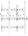
- Figure 1 is a schematic depiction of one embodiment of the present invention;
- Figure 2 is an enlarged, cross-sectional view of the embodiment shown in Figure 1 in accordance with one embodiment of the present invention;
- Figure 3 is a schematic depiction corresponding to Figure 1 in the course of reading or writing to the memory;
- Figure 4 is a schematic depiction corresponding to Figure 3 in accordance with another embodiment of the present invention;
- Figure 5 is a schematic depiction corresponding to Figure 3 of another embodiment of the present invention;
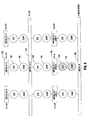
- Figure 6 is a schematic depiction of still another embodiment of the present invention;
- Figure 7 is a schematic depiction of still another embodiment of the present invention; and
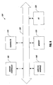
- Figure 8 is a system depiction of one embodiment of the present invention.
- Referring to Figure 1, a
crosspoint memory 10, in accordance with one embodiment of the present invention, may be implemented as a phase change memory. Thememory 10 may includeaddress lines transverse address lines - In this embodiment, pairs of adjacent transverse lines 12 define at least one cell between them including a phase change memory element 14 and a chalcogenide selection device 16. When an appropriate potential is applied between adjacent, transverse lines 12, a selection device 16, between the lines 12, turns on, allowing current flow across a memory element 14.
- While an embodiment of a crosspoint memory implemented as a phase change memory is illustrated, any other crosspoint memory may be used in other embodiments of the present invention.
- Referring to Figure 2, the phase change memory element 14 may be implemented by a series of layers provided underneath the selection device 16 in one embodiment.
Vias 18 may be provided between adjacent, but transverse lines 12, such as thelines - Thus, it may be understood from Figure 2 that shared addressing lines 12 are utilized. Namely, lines 12, such as the line 12d1, is shared between an overlying cell (including the
element 14d and theselection device 16d) and an underlying cell (including theselection device 16c and thememory element 14c). Similarly, theline 12c functions for selection of the overlying cell (including theselection device 16c and thememory element 14c), as well as for selection of thememory element 14b andselection device 16b underlying theline 12c. As a result, considerable economies may be achieved in some embodiments of the present invention, both in terms of cost and size. - In order to enable the shared addressing lines, a voltage biasing system is used. In particular, a read or write voltage V is applied. For example, a supply voltage V may be applied to the
line 12c. In this case, the selected column includes a cell made up of theselection device 16b and thememory element 14b. The selection is achieved by providing a zero voltage on theappropriate line 12b, labeled line 'B' in Figure 3, and a read or write voltage V on theline 12c in this embodiment. At the same time, unselected columns, such as thelines line 12a may also be at half the read or write voltage V (i.e., one-half V). - The potential across the cells between unselected columns and unselected rows, such as the cell made up of the (left and right)
selection device 16a and thememory element 14a, is zero. As a result, parasitic current may be significantly reduced. At the same time, the cell made up of theselection device 16b andmemory element 14b has a half voltage bias across it in one embodiment. The cells between the selected column and unselected rows have half voltage across them. Also the cells between the selected row and unselected columns have half voltage across them. But the half voltage may be such that it is insufficient to turn on theselection device 16b. Thus, there is relatively little current flow between the selected row and unselected columns and the selected column and unselected rows. In one embodiment, by maintaining the voltage difference between adjacent lines at approximately half the read or write voltage and by appropriately selecting the threshold voltage of the selection devices 16, parasitic currents can be reduced in unselected columns and read or write disturbs in unselected cells may also be reduced. - Thus, in the embodiment illustrated in Figure 3, using a one-half voltage select array biasing scheme, the unselected row lines and unselected column lines are held at the half voltage potential. The selected row line is at zero volts or ground and the selected column line is ramped to the required voltage V for the intended read or write operation. If the maximum column voltage on the selected column line is ramped to the voltage V, which may be up to the supply voltage, then the maximum voltage across an unselected element, such as an element 14 in series with the selection device 16, is half the voltage V. Sharing row and column metallizations may reduce the processing steps needed for each plane of memory in one embodiment.
- In Figure 3, the elements 14 and devices 16 are in the same polarity or orientation, such that the selection device 16 is fabricated after the memory element 14 so that the selection device 16 is on top. The read or write pulse comes in on top and the bottom line of the selected cell is held at ground. In this case, the current sources for reading and writing may be able to force current on columns or rows. In this embodiment, the current for reading and writing flows in the same direction from top to bottom for the select device and memory element. If the bottom conductive line is at ground and the top conductive line is at a positive voltage V, then current flows in a positive direction from top to bottom. If either the select device or memory device has asymmetrical iv characteristics then this method of operation would be desirable. Also it permits the same fabrication sequence (e.g. memory device on bottom (first) followed by the select device on top (last) to be utilized for all the elements).
- The selection devices 16 may be designed, in one embodiment, such that the level of voltage across the unselected cells only results in minimal parasitic leakage current and, thus, does not impact either the read or the write to the selected memory device while avoiding any disturb of unselected bits. The voltage utilized for reading a selected memory bit may be less and, thus, there may be a wider design window for the selection device 16 to avoid significant conduction during the read operation. The voltage required to write the memory element 14 may be higher and, thus, there is more of a concern of leakage to the unselected bits during the write operation. To give more margin, it may be desirable to bias the memory for read and write operations at one-third the supply voltage or to bias at one-half for reading and one-third for writing in some embodiments.
- In one embodiment, the
material 64, in Figure 2, may be a phase change material suitable for non-volatile memory data storage. The phase change material may be a material having electrical properties (e.g., resistance) that may be changed through the application of energy such as, for example, heat, light, voltage potential, or electrical current. - Examples of phase change materials may include a chalcogenide material or an ovonic material. An ovonic material may be a material that undergoes electronic or structural changes in response to an application of a voltage potential, electrical current, light, heat, etc. A chalcogenide material may be a material that includes at least one element from column VI of the periodic table or may be a material that includes one or more of the chalcogen elements, e.g., any of the elements of tellurium, sulfur, or selenium. Ovonic and chalcogenide materials may be non-volatile memory materials that may be used to store information.
- In one embodiment, the
memory material 64 may be chalcogenide element composition from the class of tellurium-germanium-antimony (TexGeySbz) material or a GeSbTe alloy, although the scope of the present invention is not limited to just these materials. - In one embodiment, if the
memory material 64 is a non-volatile, phase change material, the memory material may be programmed into one of at least two memory states by applying an electrical signal to the memory material. An electrical signal may alter the phase of the memory material between a substantially crystalline state and a substantially amorphous state, wherein the electrical resistance of thememory material 64 in the substantially amorphous state is greater than the resistance of the memory material in the substantially crystalline state. Accordingly, in this embodiment, thememory material 64 may be adapted to be altered to a particular one of a number of resistance values within a range of resistance values to provide digital or analog storage of information. - Programming of the memory material to alter the state or phase of the material may be accomplished by applying voltage potentials to the adjacent lines 12, thereby generating a voltage potential across the
memory material 64. An electrical current may flow through a portion of thememory material 64 in response to the applied voltage potentials, and may result in heating of thememory material 64. - This controlled heating and subsequent controlled cooling may alter the memory state or phase of the
memory material 64. Altering the phase or state of thememory material 64 may alter an electrical characteristic of thememory material 64. For example, resistance of the material 64 may be altered by altering the phase of thememory material 64. Either all or a portion of the phase change memory material may be altered during the writing pulse (i.e. only a portion/region ofelement 64 adjacent to either the top or bottom electrode may be phase changed during the write operation. In one embodiment primarily the portion oflayer 64 that under goes phase change is the region that is adjacent to the smaller lower electrode. Thememory material 64 may also be referred to as a programmable resistive material or simply a programmable resistance material. - In one embodiment, a voltage pulse with a potential difference of about 0.5 to 1.5 V may be applied across a portion of the memory material by applying about 0 volts to a lower line 12 and about 0.5 to 1.5 V to an upper line 12. A current flowing through the
memory material 64 in response to the applied voltage potentials may result in heating of the memory material. This heating and subsequent cooling may alter the memory state or phase of the material. - In a "reset" state, the memory material may be in an amorphous or semi-amorphous state and in a "set" state, the memory material may be in a crystalline or semi-crystalline state. The resistance of the memory material in the amorphous or semi-amorphous state may be greater than the resistance of the material in the crystalline or semi-crystalline state. The association of reset and set with amorphous and crystalline states, respectively, is a convention. Other conventions may be adopted.
- Due to electrical current, the
memory material 64 may be heated to a relatively higher temperature and then subsequently cooled at a fast rate to amorphisize memory material and "reset" memory material. Heating the volume or memory material to a relatively lower crystallization temperature may crystallize memory material and "set" memory material. Various resistances of memory material may be achieved to store information by varying the amount of current flow and duration through the volume of memory material, or by tailoring the edge rate of the trailing edge of the programming current or voltage pulse (that may impact the cooling rate of the select memory element). - The information stored in
memory material 64 may be read by measuring the resistance of the memory material. As an example, a read current may be provided to the memory material using opposed lines 12 and a resulting read voltage across the memory material may be compared against a reference voltage using, for example, the sense amplifier (not shown). The read voltage may be proportional to the resistance exhibited by the memory storage element. - In a low voltage or low field regime A, the device 16 is off and may exhibit very high resistance in some embodiments. The off resistance can, for example, range from 50,000 ohms to greater than 10 gigaohms at a bias of half the threshold voltage. The device 16 may remain in its off state until a threshold voltage VT or threshold current IT switches the device 16 to a highly conductive, low resistance on state. The voltage across the device 16 after turn on drops to a slightly lower voltage, called the holding voltage vH and remains very close to this holding voltage. In one embodiment of the present invention, as an example, the threshold voltage may be on the order of 1.1 volts and the holding voltage may be on the order of .9 volts.
- After passing through the snapback region, in the on state, the device 16 voltage drop remains close to the holding voltage as the current passing through the device is increased up to a certain, relatively high, current level. Above that current level the device remains on but displays a finite differential resistance with the voltage drop increasing with increasing current. The device 16 may remain on until the current through the device 16 is dropped below a characteristic holding current value that is dependent on the area of the material and may be impacted by the top and bottom electrodes utilized to form the device 16.
- In some embodiments of the present invention, the selection device 16 does not change phase. It remains permanently amorphous and its current-voltage characteristics may remain the same throughout its operating life.
- As an example, for a 0.5 µm diameter device 16 formed of TeAsGeSSe having respective atomic percents of 16/13/15/1/55, the holding current may be on the order of 0.1 to 100 micro-amps (µA) in one embodiment. Below this holding current, the device 16 turns off and returns to the high resistance regime at low voltage, low field. The threshold current for the device 16 may generally be of the same order as the holding current. The holding current may be altered by changing process variables, such as the top and bottom electrode material and the chalcogenide material. The device 16 may provide high "on current" for a given area of device compared to conventional access devices such as metal oxide semiconductor field effect transistors or bipolar junction transistors or semiconductor diodes.
- In some embodiments, the higher current density of the device 16 in the on state allows for higher programming current available to the memory element 14. Where the memory element 14 is a phase change memory, this enables the use of larger programming current phase change memory devices, potentially reducing the need for sub-lithographic feature structures and the commensurate process complexity, cost, process variation, and device parameter variation.
- Referring to Figure 4, the read/write current may be forced in either direction. In this case, the voltage for reading or writing is forced into the page along the line 12 (labeled "METAL N+1 LINE B,") which is transverse to direction current was forced on the
line 12c in the embodiment of Figure 3. - As shown in Figure 5, reading or writing may be done from the "bottom up". Here, the addressing
line 12a is supplied with the read or write voltage and the cell including thememory element 14a and theselection device 16a has a voltage difference sufficient to turn on theselection device 16a. Thus, while the read or write voltage is placed on theline 12a, zero volts may be placed on theline 12b (labeled "METAL N+1 LINE B"). Thus, reading or writing is possible from the top down (Figure 4) or the bottom up (Figure 5), depending on which plane of the memory is being accessed. One advantage of the embodiment of Figure 5, compared to the embodiment of Figure 4, is that it is not necessary in the embodiment of Figure 5 to have current sources for reading or writing that are able to force current in the direction into the page. - Figure 6 shows another embodiment of the present invention in which different bias voltages are utilized. In this case, the supply voltage divided by three may be utilized for biasing. The advantage of the one-third supply voltage biasing scheme in one embodiment for a single plane of memory may include increased voltage margin, since the maximum voltage across the unselected bits is now reduced to the supply voltage divided by three rather than the supply voltage divided by two. One disadvantage in some embodiments of the one-third supply voltage biasing scheme may be increased current between the unselected rows and unselected columns, since those rows and columns now have a voltage potential across them of one-third the supply voltage compared to no voltage across them per the half supply voltage bias scheme.
- In Figure 6, the read/write voltage is applied to the
line 12c and zero volts are applied to theline 12b (labeled "METAL N+1 LINE B") in one embodiment. As a result, theselection device 16b turns on, and thememory element 14b can be read or written to. The unselected lines may have a voltage of two-thirds or one third of the read/write voltage applied to them. Thus, in the case of a cell positioned between theline 12c and an unselected transverse line 12 (parallel toline 12b), a voltage difference of one-third the supply voltage is applied across the cell (V-2/3V). Also the voltage between selectedline 12b (labeled "METAL N+1 LINE B") and the bottom unselected METAL N lines is 0 - 1/3 = -1/3V. - Figure 7 corresponds to Figure 6 except now the
unselected lines 12b receive one-third the voltage V, and the lower selectedline 12a receives a voltage of zero in this embodiment. As a result, the unselected cells between the unselected Metal N+1 and the Metal N have (R-1)* C-1)cells in parallel with V/3 voltage across them. Also the unselected cells between the unselected Metal N+1 and Metal N+2 have (R-1) * (C-1) cells in parallel with V/3 voltage across them leading to standby current (where R is the number of rows and C is the number of columns). - The table set forth below provides the voltages and currents for the reset, set and read states in accordance with one embodiment of a half supply voltage bias scheme. In the tables below, "BL" may correspond to a selected
line line BL n-1 BLn BLn+1 ALL above BL WL n-1 WLn WL n+1 ALL Below WL RESET Vcc/2 100µA-1mA Vcc/2 Vcc/2 Vcc/2 0 V Vcc/2 Vcc/2 SET Vcc/2 50 µA-650 µA Vcc/2 Vcc/2 Vcc/2 0 V Vcc/2 Vcc/2 READ Vcc/2 5µA 0 100 µAVcc/2 Vcc/2 Vcc/2 0 V Vcc/2 Vcc/2 - The table below shows a corresponding arrangement for one embodiment of the one-third supply voltage biasing scheme.
BL n-1 BLn BLn+1 ALL above BL WL n-1 WLn WL n+1 ALL Below WL RESET Vcc/3 100µA-1mA Vcc/3 2/3 Vcc 2/3 Vcc 0 V 2/3 Vcc Vcc/3 SET Vcc/3 50 µA-650 µA Vcc/3 2/3 Vcc 2/3 Vcc 0 V 2/3 Vcc Vcc/3 READ Vcc/3 5µA 0 100 µAVcc/3 2/3 Vcc 2/3 Vcc 0 V 2/3 Vcc Vcc/3 - Turning to Figure 8, a portion of a
system 500 in accordance with an embodiment of the present invention is described.System 500 may be used in wireless devices such as, for example, a personal digital assistant (PDA), a laptop or portable computer with wireless capability, a web tablet, a wireless telephone, a pager, an instant messaging device, a digital music player, a digital camera, or other devices that may be adapted to transmit and/or receive information wirelessly.System 500 may be used in any of the following systems: a wireless local area network (WLAN) system, a wireless personal area network (WPAN) system, or a cellular network, although the scope of the present invention is not limited in this respect. -
System 500 may include acontroller 510, an input/output (I/O) device 520 (e.g. a keypad, display), amemory 530, awireless interface 540, and a static random access memory (SRAM) 560 and coupled to each other via abus 550. A battery 580 may supply power to thesystem 500 in one embodiment. It should be noted that the scope of the present invention is not limited to embodiments having any or all of these components. -
Controller 510 may comprise, for example, one or more microprocessors, digital signal processors, microcontrollers, or the like.Memory 530 may be used to store messages transmitted to or bysystem 500.Memory 530 may also optionally be used to store instructions that are executed bycontroller 510 during the operation ofsystem 500, and may be used to store user data. The instructions may be stored as digital information and the user data, as disclosed herein, may be stored in one section of the memory as digital data and in another section as analog memory. As another example, a given section at one time may be labeled as such and store digital information, and then later may be relabeled and reconfigured to store analog information.Memory 530 may be provided by one or more different types of memory. For example,memory 530 may comprise a volatile memory (any type of random access memory), a non-volatile memory such as a flash memory, and/orcrosspoint memory 10 illustrated in Figure 1. - The I/
O device 520 may be used to generate a message. Thesystem 500 may use thewireless interface 540 to transmit and receive messages to and from a wireless communication network with a radio frequency (RF) signal. Examples of thewireless interface 540 may include an antenna, or a wireless transceiver, such as a dipole antenna, although the scope of the present invention is not limited in this respect. Also, the I/O device 520 may deliver a voltage reflecting what is stored as either a digital output (if digital information was stored), or it may be analog information (if analog information was stored). - While an example in a wireless application is provided above, embodiments of the present invention may also be used in non-wireless applications as well.
- While the present invention has been described with respect to a limited number of embodiments, those skilled in the art will appreciate numerous modifications and variations therefrom. It is intended that the appended claims cover all such modifications and variations as fall within the scope of this present invention, as defined by the appended claims.
Claims (25)
- A method comprising:biasing first and second address lines (12) on opposite sides of a shared address line such that a first cell (12, 14) between the first address line and said shared address line is accessed and a second cell between the second address line and said shared address line is not accessed.
- The method of claim 1 including biasing a crosspoint memory (10).
- The method of claim 1 including biasing a phase change memory cell.
- The method of claim 1 including biasing a cell, including a selection device.
- The method of claim 4 including biasing a cell, including a selection device having a chalcogenide material.
- The method of claim 1 including biasing the shared address line at a first voltage, biasing the first address line at a second voltage and biasing the second line at half of said first voltage.
- The method of claim 1 including biasing the shared address line at a first voltage, biasing the first address line at a first voltage and biasing the second line at two-thirds of said first voltage.
- The method of claim 7 including biasing the shared address line at a first voltage and biasing a third line, parallel to said first address line, at one-third of said first voltage.
- The method of claim 6 including biasing the first address line at zero volts.
- The method of claim 1 including biasing a selected cell to have a first voltage difference across the selected cell and biasing an unselected cell to have a second voltage difference lower than said first voltage difference.
- The method of claim 10 including providing a selection device within said cells such that the voltage across said selected cell is sufficient to turn its selection device on, and the voltage across an unselected cell is insufficient to turn its selection device on.
- A method comprising:forming a crosspoint memory (10) comprising cells (14, 16) ;arranging a first cell and a second cell on opposite sides of a shared address line (12); andforming a selection device (16) and a memory element (14) in said first and second cells, the selection device and the memory element arranged, with respect to one another, in the same orientation in said first and second cells.
- The method of claim 12 including providing a phase change memory element in said first and second cells.
- The method of claim 12 including providing a first cell and a second cell including a selection element including a chalcogenide material.
- The method of claim 12 including enabling said shared address line to selectively access either the second cell or the first cell.
- A crosspoint memory (10) comprising:a shared address line (12);a first cell and a second cell (14, 16) on opposite sides of said shared address line;a selection device (14) and a memory element (16) in said first and second cells, said selection device and said memory element being arranged in the same orientation in both of said cells.
- The memory of claim 16 wherein said memory element is a phase change memory element.
- The memory of claim 16 wherein said selection device includes a chalcogenide material.
- The memory of claim 16 wherein said shared address line to selectively access either the first or the second cell.
- The memory of claim 16 including a first set of address lines extending in a first direction and a second set of address lines extending in a transverse direction.
- The memory of claim 20 wherein said first cell is provided between a shared address line extending in a first direction and an address line extending transversely thereto, and said second cell is defined between said shared address line and an address line extending transverse thereto.
- The memory of claim 16 wherein said selection device (14) is over said memory element (16).
- A system (500) comprising:a processor (510);an interface (540) coupled to said processor; anda crosspoint memory (530) coupled to said processor, said crosspoint memory according to any of claims 16-22.
- The system of claim 23 wherein said interface includes a dipole antenna.
- The system of claim 23 or 24, wherein said interface (540) is a wireless interface.
Priority Applications (2)
| Application Number | Priority Date | Filing Date | Title |
|---|---|---|---|
| EP04425631A EP1626411A1 (en) | 2004-08-13 | 2004-08-13 | Shared address lines for crosspoint memory |
| US11/202,428 US7359227B2 (en) | 2004-08-13 | 2005-08-11 | Shared address lines for crosspoint memory |
Applications Claiming Priority (1)
| Application Number | Priority Date | Filing Date | Title |
|---|---|---|---|
| EP04425631A EP1626411A1 (en) | 2004-08-13 | 2004-08-13 | Shared address lines for crosspoint memory |
Publications (1)
| Publication Number | Publication Date |
|---|---|
| EP1626411A1 true EP1626411A1 (en) | 2006-02-15 |
Family
ID=34932721
Family Applications (1)
| Application Number | Title | Priority Date | Filing Date |
|---|---|---|---|
| EP04425631A Withdrawn EP1626411A1 (en) | 2004-08-13 | 2004-08-13 | Shared address lines for crosspoint memory |
Country Status (2)
| Country | Link |
|---|---|
| US (1) | US7359227B2 (en) |
| EP (1) | EP1626411A1 (en) |
Families Citing this family (10)
| Publication number | Priority date | Publication date | Assignee | Title |
|---|---|---|---|---|
| JP2006260742A (en) * | 2005-02-15 | 2006-09-28 | Sanyo Electric Co Ltd | Memory |
| US7969769B2 (en) * | 2007-03-15 | 2011-06-28 | Ovonyx, Inc. | Multi-terminal chalcogenide logic circuits |
| US8679977B2 (en) | 2007-07-25 | 2014-03-25 | Micron Technology, Inc. | Method and apparatus providing multi-planed array memory device |
| US8377741B2 (en) * | 2008-12-30 | 2013-02-19 | Stmicroelectronics S.R.L. | Self-heating phase change memory cell architecture |
| US8144506B2 (en) * | 2009-06-23 | 2012-03-27 | Micron Technology, Inc. | Cross-point memory devices, electronic systems including cross-point memory devices and methods of accessing a plurality of memory cells in a cross-point memory array |
| US8693241B2 (en) * | 2011-07-13 | 2014-04-08 | SK Hynix Inc. | Semiconductor intergrated circuit device, method of manufacturing the same, and method of driving the same |
| WO2015005920A1 (en) | 2013-07-10 | 2015-01-15 | Hewlett-Packard Development Company, L.P. | Storage device write pulse control |
| US9224465B2 (en) * | 2014-03-21 | 2015-12-29 | Intel Corporation | Cross-point memory bias scheme |
| US10192616B2 (en) * | 2016-06-28 | 2019-01-29 | Western Digital Technologies, Inc. | Ovonic threshold switch (OTS) driver/selector uses unselect bias to pre-charge memory chip circuit and reduces unacceptable false selects |
| CN114822646B (en) * | 2022-04-21 | 2026-03-20 | 长江存储科技有限责任公司 | A memory device, a memory system, and a method of operation. |
Citations (4)
| Publication number | Priority date | Publication date | Assignee | Title |
|---|---|---|---|---|
| US5515311A (en) * | 1993-07-26 | 1996-05-07 | Olympus Optical Co., Ltd. | Method of driving ferroelectric memory |
| US20030027378A1 (en) * | 2000-04-28 | 2003-02-06 | Bendik Kleveland | Method for programming a threedimensional memory array incorporating serial chain diode stack |
| US20030161180A1 (en) * | 2002-02-22 | 2003-08-28 | Bloomquist Darrel R. | Shared bit lines in stacked MRAM arrays |
| US20040090809A1 (en) * | 2002-03-14 | 2004-05-13 | Tran Lung T. | Memory device array having a pair of magnetic bits sharing a common conductor line |
Family Cites Families (8)
| Publication number | Priority date | Publication date | Assignee | Title |
|---|---|---|---|---|
| US6462977B2 (en) * | 2000-08-17 | 2002-10-08 | David Earl Butz | Data storage device having virtual columns and addressing layers |
| US6643159B2 (en) * | 2002-04-02 | 2003-11-04 | Hewlett-Packard Development Company, L.P. | Cubic memory array |
| US6917532B2 (en) * | 2002-06-21 | 2005-07-12 | Hewlett-Packard Development Company, L.P. | Memory storage device with segmented column line array |
| US6759267B2 (en) * | 2002-07-19 | 2004-07-06 | Macronix International Co., Ltd. | Method for forming a phase change memory |
| US6816431B1 (en) * | 2003-05-28 | 2004-11-09 | International Business Machines Corporation | Magnetic random access memory using memory cells with rotated magnetic storage elements |
| US6965521B2 (en) * | 2003-07-31 | 2005-11-15 | Bae Systems, Information And Electronics Systems Integration, Inc. | Read/write circuit for accessing chalcogenide non-volatile memory cells |
| US6914255B2 (en) * | 2003-08-04 | 2005-07-05 | Ovonyx, Inc. | Phase change access device for memories |
| US7471552B2 (en) * | 2003-08-04 | 2008-12-30 | Ovonyx, Inc. | Analog phase change memory |
-
2004
- 2004-08-13 EP EP04425631A patent/EP1626411A1/en not_active Withdrawn
-
2005
- 2005-08-11 US US11/202,428 patent/US7359227B2/en not_active Expired - Lifetime
Patent Citations (4)
| Publication number | Priority date | Publication date | Assignee | Title |
|---|---|---|---|---|
| US5515311A (en) * | 1993-07-26 | 1996-05-07 | Olympus Optical Co., Ltd. | Method of driving ferroelectric memory |
| US20030027378A1 (en) * | 2000-04-28 | 2003-02-06 | Bendik Kleveland | Method for programming a threedimensional memory array incorporating serial chain diode stack |
| US20030161180A1 (en) * | 2002-02-22 | 2003-08-28 | Bloomquist Darrel R. | Shared bit lines in stacked MRAM arrays |
| US20040090809A1 (en) * | 2002-03-14 | 2004-05-13 | Tran Lung T. | Memory device array having a pair of magnetic bits sharing a common conductor line |
Also Published As
| Publication number | Publication date |
|---|---|
| US20060120136A1 (en) | 2006-06-08 |
| US7359227B2 (en) | 2008-04-15 |
Similar Documents
| Publication | Publication Date | Title |
|---|---|---|
| KR100504700B1 (en) | Phase random access memory with high dencity | |
| US8335100B2 (en) | Circuit, biasing scheme and fabrication method for diode accessed cross-point resistive memory array | |
| US7804082B2 (en) | Phase change memory system | |
| US7471557B2 (en) | Reading phase change memories to reduce read disturbs | |
| US7359231B2 (en) | Providing current for phase change memories | |
| US7864567B2 (en) | Programming a normally single phase chalcogenide material for use as a memory of FPLA | |
| KR100796430B1 (en) | Phase change access device for memory | |
| US7233520B2 (en) | Process for erasing chalcogenide variable resistance memory bits | |
| CN103765520B (en) | Utilize the Nonvolatile memory system of double block program | |
| US20110103134A1 (en) | Resistance random access memory having common source line | |
| US8248836B2 (en) | Non-volatile memory cell stack with dual resistive elements | |
| US20070259479A1 (en) | Forming phase change memory arrays | |
| EP1661142B1 (en) | Read bias scheme for phase change memories | |
| KR20070006608A (en) | Storage devices and semiconductor devices | |
| KR100704329B1 (en) | Method and apparatus for forming a processor-based system | |
| CN101461010A (en) | Refreshing a phase change memory | |
| US7372718B2 (en) | Storage and semiconductor device | |
| US6912146B2 (en) | Using an MOS select gate for a phase change memory | |
| JP2009526389A (en) | Memory with nanotube transistor access device | |
| US7359227B2 (en) | Shared address lines for crosspoint memory | |
| US20070171705A1 (en) | Writing phase change memories | |
| JP6352980B2 (en) | Nonvolatile memory with adjustable cell bit shape | |
| US20070238225A1 (en) | Phase change memory with improved temperature stability | |
| US10522220B2 (en) | Phase change memory device with selector MOS transistors and source line clustering |
Legal Events
| Date | Code | Title | Description |
|---|---|---|---|
| PUAI | Public reference made under article 153(3) epc to a published international application that has entered the european phase |
Free format text: ORIGINAL CODE: 0009012 |
|
| AK | Designated contracting states |
Kind code of ref document: A1 Designated state(s): AT BE BG CH CY CZ DE DK EE ES FI FR GB GR HU IE IT LI LU MC NL PL PT RO SE SI SK TR |
|
| AX | Request for extension of the european patent |
Extension state: AL HR LT LV MK |
|
| 17P | Request for examination filed |
Effective date: 20060811 |
|
| AKX | Designation fees paid |
Designated state(s): DE FR GB IT |
|
| 17Q | First examination report despatched |
Effective date: 20061012 |
|
| 17Q | First examination report despatched |
Effective date: 20061012 |
|
| RAP1 | Party data changed (applicant data changed or rights of an application transferred) |
Owner name: STMICROELECTRONICS SRL |
|
| STAA | Information on the status of an ep patent application or granted ep patent |
Free format text: STATUS: THE APPLICATION IS DEEMED TO BE WITHDRAWN |
|
| 18D | Application deemed to be withdrawn |
Effective date: 20100615 |