EP1624522A1 - Power divider and combiner in communication system - Google Patents
Power divider and combiner in communication system Download PDFInfo
- Publication number
- EP1624522A1 EP1624522A1 EP05016894A EP05016894A EP1624522A1 EP 1624522 A1 EP1624522 A1 EP 1624522A1 EP 05016894 A EP05016894 A EP 05016894A EP 05016894 A EP05016894 A EP 05016894A EP 1624522 A1 EP1624522 A1 EP 1624522A1
- Authority
- EP
- European Patent Office
- Prior art keywords
- divider
- directional
- high frequency
- way power
- wilkinson
- Prior art date
- Legal status (The legal status is an assumption and is not a legal conclusion. Google has not performed a legal analysis and makes no representation as to the accuracy of the status listed.)
- Withdrawn
Links
Images




Classifications
-
- H—ELECTRICITY
- H01—ELECTRIC ELEMENTS
- H01P—WAVEGUIDES; RESONATORS, LINES, OR OTHER DEVICES OF THE WAVEGUIDE TYPE
- H01P5/00—Coupling devices of the waveguide type
- H01P5/12—Coupling devices having more than two ports
-
- H—ELECTRICITY
- H01—ELECTRIC ELEMENTS
- H01P—WAVEGUIDES; RESONATORS, LINES, OR OTHER DEVICES OF THE WAVEGUIDE TYPE
- H01P5/00—Coupling devices of the waveguide type
- H01P5/12—Coupling devices having more than two ports
- H01P5/16—Conjugate devices, i.e. devices having at least one port decoupled from one other port
Definitions
- the present invention relates to a divider and a combiner in a communication system, and more particularly to a power divider and a combiner in a Wireless Local Area Network ('WLAN') system.
- 'WLAN' Wireless Local Area Network
- a WLAN is a data communication system that is substituted for a conventional wired LAN and allows for exchange of data by means of a radio frequency ('RF') signals, even without a wired network. That is, WLANs provide all advantages and functions of the conventional LAN technology, such as an Ethernet or a token ring, without being restrained by a wired network.
- 'RF' radio frequency
- a WLAN includes a plurality of access points ('APs') connected to a network by a wire and a plurality of stations connected to the AP wirelessly.
- the WLAN and the stations use the RF signal as a transmission medium. Accordingly, when a station frequently moves or a wire installation is difficult, the WLAN may be usefully utilized.
- the WLAN employs a Carrier Sense Multiple Access/Collisions Avoidance ('CSMA/CA') scheme as a protocol of a Media Access Control (MAC) layer.
- the CSMA/CA scheme is obtained by modifying a Carrier Sense Multiple Access/Collisions Detection ('CSMA/CD') scheme used in a wired LAN in accordance with the characteristics of the WLAN.
- 'CSMA/CD' Carrier Sense Multiple Access/Collisions Detection
- any station may transmit data regardless of sequence, data collision on a channel is detected, and data are retransmitted when data collision occurs.
- a station confirms whether or not a channel through which data are to be transmitted is being used, and the station transmits data when the channel is in an idle state.
- the station confirms availability of the channel at a preset time and then transmits data. Since the CSMA/CA scheme has no additional control message and a simple operation process as compared with the CSMA/CD scheme, the CSMA/CA scheme may be easily achieved. Therefore, the CSMA/CA scheme is being used in a WLAN system.
- the RF signal used in such a WLAN cannot penetrate a wall in a building having a steel frame structure. Further, a shift phenomenon may occur in which the frequency band of the RF signal changes due to the presence of a wall.
- FIG 1 is a view showing a general example in which a conventional WLAN AP is installed inside a steel frame building.
- the inside of the building is partitioned by walls 113, 115.
- the AP 101 and some of stations 107, 109 and 111 do not communicate with each other via an RF signal due to the presence of walls 113, 115, respectively. Therefore, since service is not provided to some of stations 107, 109 and 111, but is provided to stations 103, 105, 107, 109 and 111, a service shadow area can be said to occur.
- a method for solving the aforementioned problem includes using an RF cable, a divider and a hom antenna.
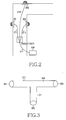
- FIG. 2 is a view showing a wall-embedded type antenna system for indoor wireless communication.
- the apparatus includes a plurality of antennas 201, 203 and 205, a divider 207 connected to the antennas 201, 203 and 205 via RF cables 211, 213 and 215, and an AP 209 connected to the divider 207 via an RF cable.
- the antennas 201, 203 and 205 are connected to the AP 209 by wire, interference between adjacent channels does not occur.
- a description on the above method has been in detail written in Korean patent application 10-2002-0062921. The system described in this application also must use the aforementioned CSMA/CA scheme.
- stations belonging to the service coverages of the second and the third antenna 203 and 205 must have knowledge of the state of each channel. However, for instance, when a multi-direction divider is not used and the station belonging to the service coverage of the first antenna 201 transmits data to the AP 209, the stations belonging to the service coverages of the second and the third antenna 203 and 205 recognize that a channel is in an idle state and can simultaneously transmit data.
- signals inputted to the second antenna 203 and the third antenna 205 are simultaneously transmitted to the AP 209 through the RF cables, data disruption can occur.
- Such an anomaly is called a hidden node problem.
- the divider 207 since it has been considered that the divider 207 only distributes power from the AP 209 to the antennas 201, 203 and 205, the divider 207 cannot be applied to the CSMA/CA scheme.
- a divider is very important.
- a divider generally used includes a T junction divider, a resistive power divider and a Wilkinson power divider.
- FIG. 3 is a view showing a conventional T junction divider.
- the T junction divider is a simple divider manufactured by dividing a line. Since the T junction divider can distribute power in omni-directions through ports 301, 303 and 305, the T junction divider can be applied to the system using the CSMA/CA scheme. However, since resistors are not used in lines 307, 309 and 311, the T junction divider has no loss of input power. However, since impedance matching in all ports is impossible, loss due to power reflection occurs.
- FIG. 4 is a circuit diagram showing a resistive power divider.
- the resistive power divider is manufactured by coupling resistive elements 407, 409 and 411 to ports 401, 403 and 405, respectively.
- the resistive power divider In the resistive power divider, the loss of input power occurs due to the resistive elements 407, 409 and 411.
- a desired power distribution ratio can be obtained and matching can be accomplished in all ports.
- the resistive power divider can distribute power in omni-directions just as the T junction divider.
- FIG. 5 is a circuit diagram showing a conventional Wilkinson power divider.
- the Wilkinson power divider is a power divider mainly used in an RF band or a micro frequency band.
- the Wilkinson power divider includes an input port 501, outputs ports 503 and 505, quarter wave microstrip lines 507 and 509 for port matching, and a balance resistor 511.
- the Wilkinson power divider uses the balance resistor 511 for port matching in an odd mode. Further, the Wilkinson power divider includes the balance resistor 511 for port matching in the odd mode connected in parallel to a power distribution port, the Wilkinson power divider has a high frequency characteristic and a power characteristic superior to those of the resistive power divider.
- the present invention has been made to solve the abovementioned problems occurring in conventional systems.
- a high frequency omni-directional 2-way power divider which includes one input terminal and two output terminals so that a signal inputted through the input terminal is uniformly distributed to the two output terminals, with the high frequency omni-directional 2-way power divider including: a first Wilkinson regular divider including one input terminal and a first and a second output terminal; a second Wilkinson regular divider including one input terminal and a third and a fourth output terminal, the third output terminals being connected to the first output terminal of the first Wilkinson regular divider; and a third Wilkinson regular divider including one input terminal and a fifth and a sixth output terminal, the fifth output terminal being connected to the second output terminal of the second Wilkinson regular divider and the sixth output terminal being connected to the fourth output terminal of the second Wilkinson regular divider.
- each of the quarter wave microstrip lines has a characteristic impedance of 70.7 ⁇ and a balance resistor has a value of 100 ⁇ .
- each of the input terminals has a characteristic impedance of 50 ⁇ .
- a high frequency omni-directional 3-way power divider which includes one input terminal and three output terminals so that a signal inputted through the input terminal is uniformly distributed to the three output terminals
- the high frequency omni-directional 3-way power divider including a first and a second high frequency 2-way divider, each of the first and the second high frequency 2-way dividers includes a Wilkinson regular divider having one input terminal and first and second output terminals; a first Wilkinson irregular divider having one input terminal and a first and a second output terminal, the first output terminal of the first Wilkinson irregular divider being connected to the first output terminal of the Wilkinson regular divider, a second Wilkinson irregular divider having one input terminal and first and second output terminals, the first output terminal of the second Wilkinson irregular divider being connected to the second output terminal of the Wilkinson regular divider, the second output terminal of the second Wilkinson irregular divider being connected to the second output terminal of the first output terminal of the first
- the high frequency omni-directional 3-way power divider distributes power by -9dB from one input terminal to remaining input terminals.
- power of -4.5 dB is distributed to each of the input terminals of the Wilkinson irregular dividers at a point at which input terminals of the Wilkinson regular dividers in the first and the second high frequency 2-way divider are connected with each other.
- a divider proposed through the present invention which will be described later not only uniformly distributes a signal through any port but also minimizes power loss.
- the apparatus proposed in the present invention will be called an omni-directional n-way power divider/combiner.
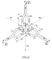
- FIG. 6 is a view showing an omni-directional 2-way power divider according to a first preferred embodiment of the present invention.
- the omni-directional 2-way power divider includes three input/output ports, that is, a first port 601, a second port 603 and a third port 605, six quarter wave microstrip lines 607, 609, 611. 613, 615 and 617, and three balance resistors 619, 621 and 623.
- Dotted lines 625, 627 and 629 in FIG. 6 are reference lines provided for analyzing the omni-directional 2-way power divider.
- the ports 601, 603 and 605 each have a characteristic impedance of 50 ⁇ .
- FIG 7a is a circuit diagram showing an odd mode equivalent circuit for the ports 601 and 603 obtained by dividing the omni-directional 2-way power divider of FIG. 6 with respect to the reference line 625.
- the portion in contact with the reference line 625 is short-circuited and the resistance of the balance resistor 619 cut by the reference line 625 becomes 50 ⁇ which corresponds to 1/2 of the original resistance.
- the quarter wave microstrip lines 609 and 611 of FIG. 6 represent quarter wave microstrip lines 703 and 705 of FIG 7a respectively, and the balance resistors 619 and 621 of FIG. 6 represent resistors 709 and 707 of FIG. 7a. Further, when the characteristic of a wave microstrip line is considered, the quarter wave microstrip line 607 of FIG. 6 can be omitted due to a short of the first port 601.
- the quarter wave microstrip line 703 of FIG. 7a can be omitted because electric current does not flow in the quarter wave microstrip line 703. Consequently, the equivalent circuit of FIG. 7a can be more simply shown as FIG. 7b.
- the equivalent circuit of FIG. 7b includes a quarter wave microstrip line 711 and three resistors 713, 715 and 717.
- impedance of a port 2 direction at a point 721 has a value of 100 ⁇ by the quarter wave microstrip line 711 and a resistor 713 of the port 2.
- impedance viewed at a point 723 is 50 ⁇ because the resistance 100 ⁇ viewed at the point 721 is connected in parallel to a resistor 715. Accordingly, it can be understood that impedance matching is accomplished.
- FIG. 8a is a circuit diagram showing an even mode equivalent circuit for the ports 601 and 603 obtained by dividing the omni-directional 2-way power divider of FIG. 6 with respect to the reference dotted line 625.
- a portion of FIG 6 in contact with the reference dotted line 625 is opened.
- the resistance of the balance resistor 619 cut by the reference dotted line 625 becomes 50 ⁇ which corresponds to 1/2 of the original resistance, similar to the odd mode.
- the even mode equivalent circuit of FIG. 8a includes two quarter wave microstrip lines 801 and 803 and three resistors 805, 807 and 809.
- a ABCD parameter and a Y parameter for the quarter wave microstrip line 803 and the resistor 807 of a lower portion may be expressed by the following Equations 1 and 2, respectively.
- a total Y parameter of the Y parameter for the quarter wave microstrip line 801 of the upper portion and the Y parameter for the quarter wave microstrip line 803 and the resistor 807 of the lower portion may be expressed by sum of the above Equations 2 and 4 because the quarter wave microstrip line 801 is connected in parallel to the quarter wave microstrip line 803 and the resistor 807.
- FIG 8b is an equivalent circuit obtained by simplifying the equivalent circuit of FIG 8a by the total ABCD parameter.
- impedance of a port 2 direction at a point 819 has a value of 25 ⁇ by an input resistor 811 and a quarter wave microstrip line 813 of the port 2.
- impedance at a point 821 is 50 ⁇ . Accordingly, it can be understood that impedance matching is accomplished.
- FIG. 9 is a graph illustrating a design result of the omni-directional 2-way power divider according to the preferred embodiment of the present invention.
- S 11 , S 22 , S 33 each show a power level smaller than -80 dB at 1 GHz, it can be understood that impedance matching is accomplished in each port.
- S 12 , S 13 , S 21 , S 23 , S 31 , S 32 each show a power level of about -6 dB. Accordingly, as shown in the design result, it can be understood that the omni-directional 2-way power divider according to the present invention enables signal transmission between any ports while maintaining impedance matching in all ports.
- an omni-directional 3-way power divider according to a second embodiment of the present invention is similar to the omni-directional 2-way power divider, the omni-directional 3-way power divider will be briefly described hereinafter.
- FIG. 10 is a circuit diagram showing the omni-directional 3-way power divider.
- the omni-directional 3-way power divider is constructed by connecting two omni-directional 2-way power dividers 1011 and 1013 with each other.
- power of -4.5 dB is distributed in each of the ports 1001, 1003, 1005 and 1007 and toward each of the ports in a point 1009 at which the omni-directional 2-way power dividers 1011 and 1013 are connected to each other, so that power of -9 dB is distributed in each of the ports 1001, 1003, 1005 and 1007.
- quarter wave microstrip lines 1019, 1021, 1027 and 1037 are added to the two omni-directional 2-way power dividers, so that power can be uniformly distributed, thereby enabling an expansion to the omni-directional 3-way power divider.
Landscapes
- Variable-Direction Aerials And Aerial Arrays (AREA)
- Amplifiers (AREA)
Abstract
Description
- The present invention relates to a divider and a combiner in a communication system, and more particularly to a power divider and a combiner in a Wireless Local Area Network ('WLAN') system.
- Generally, a WLAN is a data communication system that is substituted for a conventional wired LAN and allows for exchange of data by means of a radio frequency ('RF') signals, even without a wired network. That is, WLANs provide all advantages and functions of the conventional LAN technology, such as an Ethernet or a token ring, without being restrained by a wired network.
- A WLAN includes a plurality of access points ('APs') connected to a network by a wire and a plurality of stations connected to the AP wirelessly. The WLAN and the stations use the RF signal as a transmission medium. Accordingly, when a station frequently moves or a wire installation is difficult, the WLAN may be usefully utilized.
- The WLAN employs a Carrier Sense Multiple Access/Collisions Avoidance ('CSMA/CA') scheme as a protocol of a Media Access Control (MAC) layer. The CSMA/CA scheme is obtained by modifying a Carrier Sense Multiple Access/Collisions Detection ('CSMA/CD') scheme used in a wired LAN in accordance with the characteristics of the WLAN. In the CSMA/CD scheme, any station may transmit data regardless of sequence, data collision on a channel is detected, and data are retransmitted when data collision occurs. In contrast, in the CSMA/CA scheme, a station confirms whether or not a channel through which data are to be transmitted is being used, and the station transmits data when the channel is in an idle state. However, when the channel is being used, the station confirms availability of the channel at a preset time and then transmits data. Since the CSMA/CA scheme has no additional control message and a simple operation process as compared with the CSMA/CD scheme, the CSMA/CA scheme may be easily achieved. Therefore, the CSMA/CA scheme is being used in a WLAN system.
- In consideration of the characteristics of an RF signal, the RF signal used in such a WLAN cannot penetrate a wall in a building having a steel frame structure. Further, a shift phenomenon may occur in which the frequency band of the RF signal changes due to the presence of a wall.
- FIG 1 is a view showing a general example in which a conventional WLAN AP is installed inside a steel frame building.
- Referring to FIG. 1, the inside of the building is partitioned by
walls stations walls stations stations - A method for solving the aforementioned problem includes using an RF cable, a divider and a hom antenna.
- FIG. 2 is a view showing a wall-embedded type antenna system for indoor wireless communication. Referring to FIG. 2, the apparatus includes a plurality of
antennas divider 207 connected to theantennas RF cables AP 209 connected to thedivider 207 via an RF cable. In the apparatus, since theantennas AP 209 by wire, interference between adjacent channels does not occur. A description on the above method has been in detail written in Korean patent application 10-2002-0062921. The system described in this application also must use the aforementioned CSMA/CA scheme. In order for the prior application to use the CSMA/CA scheme, when a station belonging to the service coverage of thefirst antenna 201 transmits data, stations belonging to the service coverages of the second and thethird antenna first antenna 201 transmits data to the AP 209, the stations belonging to the service coverages of the second and thethird antenna second antenna 203 and thethird antenna 205 are simultaneously transmitted to theAP 209 through the RF cables, data disruption can occur. Such an anomaly is called a hidden node problem. However, since it has been considered that thedivider 207 only distributes power from theAP 209 to theantennas divider 207 cannot be applied to the CSMA/CA scheme. - In order to solve the above-described problem, a divider is very important. A divider generally used includes a T junction divider, a resistive power divider and a Wilkinson power divider.
- FIG. 3 is a view showing a conventional T junction divider. The T junction divider is a simple divider manufactured by dividing a line. Since the T junction divider can distribute power in omni-directions through
ports lines - FIG. 4 is a circuit diagram showing a resistive power divider. The resistive power divider is manufactured by coupling
resistive elements ports resistive elements outputs ports wave microstrip lines distribution outputs ports - Accordingly, the present invention has been made to solve the abovementioned problems occurring in conventional systems.
- It is the object of the present invention to provide a power divider capable of uniformly and omni-directionally distributing input power while minimizing the loss of the input power.
- This object is solved by the subject matter of the independent claims.
- Preferred embodiments are defined in the dependent claims.
- It is an aspect of the present invention to provide a power divider capable of enabling signal transmission between any ports while maintaining impedance matching in all ports.
- In order to accomplish the above, according to one aspect of the present, there is provided a high frequency omni-directional 2-way power divider which includes one input terminal and two output terminals so that a signal inputted through the input terminal is uniformly distributed to the two output terminals, with the high frequency omni-directional 2-way power divider including: a first Wilkinson regular divider including one input terminal and a first and a second output terminal; a second Wilkinson regular divider including one input terminal and a third and a fourth output terminal, the third output terminals being connected to the first output terminal of the first Wilkinson regular divider; and a third Wilkinson regular divider including one input terminal and a fifth and a sixth output terminal, the fifth output terminal being connected to the second output terminal of the second Wilkinson regular divider and the sixth output terminal being connected to the fourth output terminal of the second Wilkinson regular divider.
- According to the present invention, when one of the three input terminals contained in the first to the third Wilkinson regular dividers is used as the input terminal of the 2-way power divider, other two input terminals are used as output terminals to which power is uniformly distributed.
- According to the present invention, each of the quarter wave microstrip lines has a characteristic impedance of 70.7Ω and a balance resistor has a value of 100Ω.
- According to the present invention, each of the input terminals has a characteristic impedance of 50Ω.
- In order to accomplish the aforementioned objects, according to one aspect of the present invention, there is provided a high frequency omni-directional 3-way power divider which includes one input terminal and three output terminals so that a signal inputted through the input terminal is uniformly distributed to the three output terminals, the high frequency omni-directional 3-way power divider including a first and a second high frequency 2-way divider, each of the first and the second high frequency 2-way dividers includes a Wilkinson regular divider having one input terminal and first and second output terminals; a first Wilkinson irregular divider having one input terminal and a first and a second output terminal, the first output terminal of the first Wilkinson irregular divider being connected to the first output terminal of the Wilkinson regular divider, a second Wilkinson irregular divider having one input terminal and first and second output terminals, the first output terminal of the second Wilkinson irregular divider being connected to the second output terminal of the Wilkinson regular divider, the second output terminal of the second Wilkinson irregular divider being connected to the second output terminal of the first Wilkinson irregular divider; a first quarter wave microstrip line connected to a point at which the first terminal of the Wilkinson regular divider is connected to the first output terminal of the first Wilkinson irregular divider; and a second quarter wave microstrip line connected to a point at which the second terminal of the Wilkinson regular divider is connected to the first output terminal of the second Wilkinson irregular divider, wherein, input terminals of the Wilkinson regular dividers of the first and the second high frequency 2-way divider are connected with each other, and wherein, when one of the input terminals contained in the first and the second high frequency 2-way divider is used as the input terminal of the high frequency omni-directional 3-way power divider, other three input terminals are used as output terminals to which power is uniformly distributed.
- According to the present invention, the high frequency omni-directional 3-way power divider distributes power by -9dB from one input terminal to remaining input terminals.
- According to the present invention, power of -4.5 dB is distributed to each of the input terminals of the Wilkinson irregular dividers at a point at which input terminals of the Wilkinson regular dividers in the first and the second high frequency 2-way divider are connected with each other.
- The above object and other aspects, features and advantages of the present invention will be more apparent from the following detailed description taken in conjunction with the accompanying drawings, in which:
- FIG. 1 is a view showing a general example in which a conventional WLAN AP is installed inside a steel frame building;
- FIG. 2 is a view showing a wall-embedded type antenna system for indoor wireless communication;
- FIG. 3 is a view showing a T Junction divider;
- FIG. 4 is a circuit diagram showing a conventional resistive power divider;
- FIG 5 is a circuit diagram showing a conventional Wilkinson power divider;
- FIG. 6 is a view showing an omni-directional 2-way power divider according to a first preferred embodiment of the present invention;
- FIGs. 7a and 7b are equivalent circuit diagrams in an odd mode in an omni-directional 2-way power divider according to the first preferred embodiment of the present invention;
- FIGs. 8a and 8b are equivalent circuit diagrams in an even mode in an omni-directional 2-way power divider according to a preferred embodiment of the present invention;
- FIG 9 is a graph illustrating a design result of an omni-directional 2-way power divider according to the preferred embodiment of the present invention; and
- FIG 10 is a circuit diagram showing an omni-directional 3-way power divider according to a second preferred embodiment of the present invention.
- Hereinafter, preferred embodiments of the present invention will be described with reference to the accompanying drawings. A divider proposed through the present invention which will be described later not only uniformly distributes a signal through any port but also minimizes power loss. The apparatus proposed in the present invention will be called an omni-directional n-way power divider/combiner.
- In a detailed description provided below, two representative embodiments of the present invention are described that achieve the aforementioned technical subject. First, an omni-directional 2-way power divider of the present invention is described. Next, an omni-directional 3-way power divider is briefly described. It will be apparent to those of skill in the art that the power divider can be extended to an n-way power divider. Further, since a divider becomes a combiner by differently applying an input/output, a divider-centered description is given in the present invention.
- FIG. 6 is a view showing an omni-directional 2-way power divider according to a first preferred embodiment of the present invention. Referring to FIG. 6, the omni-directional 2-way power divider includes three input/output ports, that is, a
first port 601, asecond port 603 and athird port 605, six quarterwave microstrip lines balance resistors Dotted lines ports - Hereinafter, an odd mode and an even mode are described for analysis of the omni-directional 2-way power divider according to the preferred embodiment of the present invention.
- FIG 7a is a circuit diagram showing an odd mode equivalent circuit for the
ports reference line 625. Herein, in an analysis based on the odd mode, the portion in contact with thereference line 625 is short-circuited and the resistance of thebalance resistor 619 cut by thereference line 625 becomes 50Ω which corresponds to 1/2 of the original resistance. - By the above condition, the quarter
wave microstrip lines wave microstrip lines balance resistors resistors wave microstrip line 607 of FIG. 6 can be omitted due to a short of thefirst port 601. - In consideration of the characteristic of the odd mode, the quarter
wave microstrip line 703 of FIG. 7a can be omitted because electric current does not flow in the quarterwave microstrip line 703. Consequently, the equivalent circuit of FIG. 7a can be more simply shown as FIG. 7b. - The equivalent circuit of FIG. 7b includes a quarter
wave microstrip line 711 and threeresistors port 2 direction at apoint 721 has a value of 100Ω by the quarterwave microstrip line 711 and a resistor 713 of theport 2. Further, impedance viewed at apoint 723 is 50Ω because the resistance 100Ω viewed at thepoint 721 is connected in parallel to aresistor 715. Accordingly, it can be understood that impedance matching is accomplished. - FIG. 8a is a circuit diagram showing an even mode equivalent circuit for the
ports line 625. Herein, in an analysis based on the even mode, a portion of FIG 6 in contact with the reference dottedline 625 is opened. Further, the resistance of thebalance resistor 619 cut by the reference dottedline 625 becomes 50Ω which corresponds to 1/2 of the original resistance, similar to the odd mode. - Referring to FIG 8a, the even mode equivalent circuit of FIG. 8a includes two quarter
wave microstrip lines resistors wave microstrip line 803 and theresistor 807 of a lower portion may be expressed by the followingEquations 

- Next, in FIG. 8a, a ABCD parameter and a Y parameter for the quarter
wave microstrip line 801 of an upper portion may be expressed by the followingEquations 3 and 4, respectively.

- In FIG. 8a, a total Y parameter of the Y parameter for the quarter
wave microstrip line 801 of the upper portion and the Y parameter for the quarterwave microstrip line 803 and theresistor 807 of the lower portion may be expressed by sum of theabove Equations 2 and 4 because the quarterwave microstrip line 801 is connected in parallel to the quarterwave microstrip line 803 and theresistor 807.
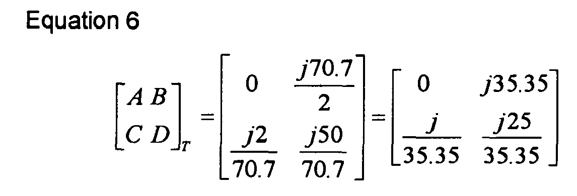
- FIG 8b is an equivalent circuit obtained by simplifying the equivalent circuit of FIG 8a by the total ABCD parameter. Referring to FIG. 8b, impedance of a
port 2 direction at apoint 819 has a value of 25Ω by aninput resistor 811 and a quarterwave microstrip line 813 of theport 2. Further, because the impedance viewed at thepoint 819 is connected in series to aresistor 815, impedance at apoint 821 is 50Ω. Accordingly, it can be understood that impedance matching is accomplished. - It will be recognized that the aforementioned method can be similarly applied to the
reference points second port 603 and thethird port 605. - An S parameter of the omni-directional 2-way power divider of the present invention may be expressed by the following Equation 7.


- As shown in the above Equation 7, in the omni-directional 2-way power divider according to the present invention, since impedance matching is accomplished in the three ports, a value of S11, S22, S33 becomes 0. Further, it can be understood that the other power is uniformly distributed.
- Further, in the divider, matching is accomplished in each port and signal transmission between adjacent ports is possible.
- FIG. 9 is a graph illustrating a design result of the omni-directional 2-way power divider according to the preferred embodiment of the present invention. Referring to FIG. 9, since S11, S22, S33 each show a power level smaller than -80 dB at 1 GHz, it can be understood that impedance matching is accomplished in each port. Further, S12, S13, S21, S23, S31, S32 each show a power level of about -6 dB. Accordingly, as shown in the design result, it can be understood that the omni-directional 2-way power divider according to the present invention enables signal transmission between any ports while maintaining impedance matching in all ports.
- Next, since an omni-directional 3-way power divider according to a second embodiment of the present invention is similar to the omni-directional 2-way power divider, the omni-directional 3-way power divider will be briefly described hereinafter.
- FIG. 10 is a circuit diagram showing the omni-directional 3-way power divider. Referring to FIG. 10, the omni-directional 3-way power divider is constructed by connecting two omni-directional 2-
way power dividers ports point 1009 at which the omni-directional 2-way power dividers ports way power dividers wave microstrip lines way power divider 1011, two quarterwave microstrip lines way power divider 1013, and then the values of the quarterwave microstrip lines 
- As shown in the above Equation 8, power is uniformly distributed to all ports.
- Finally, four quarter
wave microstrip lines - While the invention has been shown and described with reference to certain preferred embodiments, it will be understood by those skilled in the art that various changes in form and details may be made therein without departing from the scope of the invention as defined by the appended claims.
Claims (10)
- A high frequency omni-directional 2-way power divider which includes one input terminal and two output terminals so that a signal inputted is uniformly distributed to the two output terminals, the high frequency omni-directional 2-way power divider comprising:a first divider including one input terminal and first and second output terminals;a second divider including one input terminal and third and fourth output terminals, the third output terminal being connected to the first output terminal of the first divider, anda third divider including one input terminal and fifth and sixth output terminals, the fifth output terminal being connected to the second output terminal of the first divider and the sixth output terminal being connected to the fourth output terminal of the second divider,wherein, when one of the three input terminals contained in the first to the third divider is used as the input terminal of the 2-way power divider, the other two input terminals function as output terminals to which power is uniformly distributed.
- The high frequency omni-directional 2-way power divider as claimed in claim 1, wherein said first divider, second divider and third divider are a first Wilkinson regular, second Wilkinson regular divider and third Wilkinson regular divider respectively.
- The high frequency omni-directional 2-way power divider as claimed in claim 1 or 2, wherein each divider includes two quarter wave microstrip lines and one balance resistor.
- The high frequency omni-directional 2-way power divider as claimed in claim 3, wherein each of the two quarter wave microstrip lines has a characteristic impedance of 70.7Ω.
- The high frequency omni-directional 2-way power divider as claimed in claim 3, wherein the balance resistor has a value of 100Ω .
- The high frequency omni-directional 2-way power divider as claimed in one of claims 1 to 5, wherein each input terminal has a characteristic impedance of 50Ω.
- A high frequency omni-directional 3-way power divider which includes one input terminal and three output terminals so that a signal inputted is uniformly distributed to the three output terminals, the high frequency omni-directional 3-way power divider comprising a first and a second high frequency omni-directional 2-way power divider, each of the first and the second high frequency omni-directional 2-way power dividers comprising:a regular divider having one input terminal and first and second output terminals;a first irregular divider having one input terminal and first and second output terminals, the first output terminal of the first irregular divider being connected to the first output terminal of the regular divider;a second irregular divider having one input terminal and first and second output terminals, the first output terminal of the second irregular divider being connected to the second output terminal of the regular divider, the second output terminal of the second irregular divider being connected to the second output terminal of the first irregular divider,a first quarter wave microstrip line connected to a point at which the first terminal of the regular divider is connected to the first output terminal of the first irregular divider, anda second quarter wave microstrip line connected to a point at which the second terminal of the regular divider is connected to the first output terminal of the second irregular divider,wherein, input terminals of the regular divider and of the first and the second dividers are connected with each other, andwherein, when one of the input terminals contained in the first and the second dividers is used as the input terminal of the high frequency omni-directional 3-way power divider, the other three input terminals function as output terminals to which power is uniformly distributed.
- The high frequency omni-directional 3-way power divider as claimed in claim 7, wherein said regular divider is a Wilkinson regular divider, said first irregular divider is a first Wilkinson irregular divider, and said second irregular divider is a second Wilkinson irregular divider.
- The high frequency omni-directional 3-way power divider as claimed in claim 7 or 8, wherein the high frequency omni-directional 3-way power divider distributes power by -9 dB from one input terminal to the remaining input terminals.
- The high frequency omni-directional 3-way power divider as claimed in claim 6, wherein power of -4.5 dB is distributed to each of the input terminals of the Wilkinson irregular dividers at a point at which input terminals of the Wilkinson regular dividers in the first and the second high frequency 2-way divider are connected with each other.
Applications Claiming Priority (1)
| Application Number | Priority Date | Filing Date | Title |
|---|---|---|---|
| KR1020040061395A KR100754635B1 (en) | 2004-08-04 | 2004-08-04 | Power Dividers / Synthesizers in Communication Systems |
Publications (1)
| Publication Number | Publication Date |
|---|---|
| EP1624522A1 true EP1624522A1 (en) | 2006-02-08 |
Family
ID=35159806
Family Applications (1)
| Application Number | Title | Priority Date | Filing Date |
|---|---|---|---|
| EP05016894A Withdrawn EP1624522A1 (en) | 2004-08-04 | 2005-08-03 | Power divider and combiner in communication system |
Country Status (3)
| Country | Link |
|---|---|
| US (1) | US7205865B2 (en) |
| EP (1) | EP1624522A1 (en) |
| KR (1) | KR100754635B1 (en) |
Cited By (2)
| Publication number | Priority date | Publication date | Assignee | Title |
|---|---|---|---|---|
| FR2970816A1 (en) * | 2011-01-24 | 2012-07-27 | St Microelectronics Sa | RADIOFREQUENCY COMBINER |
| FR2970817A1 (en) * | 2011-01-24 | 2012-07-27 | St Microelectronics Sa | RADIOFREQUENCY SEPARATOR |
Families Citing this family (14)
| Publication number | Priority date | Publication date | Assignee | Title |
|---|---|---|---|---|
| KR100998309B1 (en) | 2009-02-27 | 2010-12-03 | 주식회사 에이스테크놀로지 | How to design a power divider |
| US8216912B2 (en) | 2009-08-26 | 2012-07-10 | International Business Machines Corporation | Method, structure, and design structure for a through-silicon-via Wilkinson power divider |
| US8928429B2 (en) | 2011-05-17 | 2015-01-06 | City University Of Hong Kong | Multiple-way ring cavity power combiner and divider |
| US9503133B2 (en) | 2012-12-03 | 2016-11-22 | Dockon Ag | Low noise detection system using log detector amplifier |
| US9263787B2 (en) | 2013-03-15 | 2016-02-16 | Dockon Ag | Power combiner and fixed/adjustable CPL antennas |
| US9048943B2 (en) | 2013-03-15 | 2015-06-02 | Dockon Ag | Low-power, noise insensitive communication channel using logarithmic detector amplifier (LDA) demodulator |
| JP6416195B2 (en) | 2013-03-15 | 2018-10-31 | ドックオン エージー | Frequency selective logarithmic amplifier with natural frequency demodulation capability |
| US9236892B2 (en) | 2013-03-15 | 2016-01-12 | Dockon Ag | Combination of steering antennas, CPL antenna(s), and one or more receive logarithmic detector amplifiers for SISO and MIMO applications |
| US11183974B2 (en) | 2013-09-12 | 2021-11-23 | Dockon Ag | Logarithmic detector amplifier system in open-loop configuration for use as high sensitivity selective receiver without frequency conversion |
| US11082014B2 (en) | 2013-09-12 | 2021-08-03 | Dockon Ag | Advanced amplifier system for ultra-wide band RF communication |
| WO2015038191A1 (en) | 2013-09-12 | 2015-03-19 | Dockon Ag | Logarithmic detector amplifier system for use as high sensitivity selective receiver without frequency conversion |
| CN107947755B (en) * | 2016-10-11 | 2021-06-29 | 康普技术有限责任公司 | energy absorption circuit |
| CN108511888B (en) | 2017-02-28 | 2020-12-08 | 华为技术有限公司 | An antenna and communication equipment |
| CN112313831B (en) * | 2019-05-29 | 2023-02-21 | 松下知识产权经营株式会社 | Three distributors |
Citations (4)
| Publication number | Priority date | Publication date | Assignee | Title |
|---|---|---|---|---|
| US2784381A (en) * | 1948-10-05 | 1957-03-05 | Bell Telephone Labor Inc | Hybrid ring coupling arrangements |
| US3701056A (en) * | 1969-08-25 | 1972-10-24 | Iwatsu Electric Co Ltd | Resistive film bleeder resistor for use in an branch circuit |
| US5455546A (en) * | 1994-09-22 | 1995-10-03 | Glenayre Electronics, Inc. | High power radio frequency divider/combiner |
| US20020158706A1 (en) * | 1999-03-09 | 2002-10-31 | Edwards David John | Degenerate mode combiner |
Family Cites Families (10)
| Publication number | Priority date | Publication date | Assignee | Title |
|---|---|---|---|---|
| US3963990A (en) * | 1974-02-27 | 1976-06-15 | Communications Satellite Corporation (Comsat) | Interference reduction circuit |
| US4419636A (en) * | 1981-10-22 | 1983-12-06 | Hong Yu | Low frequency wide band signal coupler |
| US4679010A (en) * | 1985-12-20 | 1987-07-07 | Itt Gallium Arsenide Technology Center, A Division Of Itt Corporation | Microwave circulator comprising a plurality of directional couplers connected together by isolation amplifiers |
| US4875024A (en) * | 1988-12-05 | 1989-10-17 | Ford Aerospace Corporation | Low loss power splitter |
| FR2666186B1 (en) * | 1990-08-24 | 1994-05-06 | Etat Francais Cnet | BIDIRECTIONAL DUPLEXER FOR POLARIZED HYPERFREQUENCY WAVES REALIZABLE IN PARTICULAR IN MONOLITHIC TECHNOLOGY ON GALLIUM ARSENIDE. |
| KR100287062B1 (en) * | 1997-12-26 | 2001-04-16 | 정선종 | Plannar four-way power divider with eight-port |
| JP2000216606A (en) * | 1998-12-09 | 2000-08-04 | Ricoh Co Ltd | Power distribution combiner |
| JP2003518262A (en) | 1999-10-06 | 2003-06-03 | ワーナー・ミュージック・グループ・インコーポレイテッド | Recording and playback control system |
| KR20020072021A (en) * | 2001-03-08 | 2002-09-14 | 주식회사 흥창 | Power divider/combiner |
| JP3592264B2 (en) * | 2001-06-22 | 2004-11-24 | 埼玉日本電気株式会社 | Power distribution combining method and power distribution combining circuit |
-
2004
- 2004-08-04 KR KR1020040061395A patent/KR100754635B1/en not_active Expired - Fee Related
-
2005
- 2005-03-14 US US11/080,006 patent/US7205865B2/en not_active Expired - Fee Related
- 2005-08-03 EP EP05016894A patent/EP1624522A1/en not_active Withdrawn
Patent Citations (4)
| Publication number | Priority date | Publication date | Assignee | Title |
|---|---|---|---|---|
| US2784381A (en) * | 1948-10-05 | 1957-03-05 | Bell Telephone Labor Inc | Hybrid ring coupling arrangements |
| US3701056A (en) * | 1969-08-25 | 1972-10-24 | Iwatsu Electric Co Ltd | Resistive film bleeder resistor for use in an branch circuit |
| US5455546A (en) * | 1994-09-22 | 1995-10-03 | Glenayre Electronics, Inc. | High power radio frequency divider/combiner |
| US20020158706A1 (en) * | 1999-03-09 | 2002-10-31 | Edwards David John | Degenerate mode combiner |
Non-Patent Citations (2)
| Title |
|---|
| D'AGOSTINO S ET AL: "Innovative power distributed amplifier using the Wilkinson combiner", 1 April 1995, IEE PROCEEDINGS: MICROWAVES, ANTENNAS AND PROPAGATION, IEE, STEVENAGE, HERTS, GB, PAGE(S) 97-101, ISSN: 1350-2417, XP006004215 * |
| WELLER T M ET AL: "Membrane technology (MIST-T) applied to microstrip: a 33 GHz Wilkinson power divider", 23 May 1994, MICROWAVE SYMPOSIUM DIGEST, 1994., IEEE MTT-S INTERNATIONAL SAN DIEGO, CA, USA 23-27 MAY 1994, NEW YORK, NY, USA,IEEE, PAGE(S) 911-914, ISBN: 0-7803-1778-5, XP010586438 * |
Cited By (6)
| Publication number | Priority date | Publication date | Assignee | Title |
|---|---|---|---|---|
| FR2970816A1 (en) * | 2011-01-24 | 2012-07-27 | St Microelectronics Sa | RADIOFREQUENCY COMBINER |
| FR2970817A1 (en) * | 2011-01-24 | 2012-07-27 | St Microelectronics Sa | RADIOFREQUENCY SEPARATOR |
| US8712466B2 (en) | 2011-01-24 | 2014-04-29 | Stmicroelectronics Sa | Radio frequency splitter |
| US8843087B2 (en) | 2011-01-24 | 2014-09-23 | Stmicroelectronics Sa | Radio frequency combiner |
| US9231642B2 (en) | 2011-01-24 | 2016-01-05 | Stmicroelectronics Sa | Radio frequency splitter |
| US9853345B2 (en) | 2011-01-24 | 2017-12-26 | Stmicroelectronics Sa | Radio frequency splitter |
Also Published As
| Publication number | Publication date |
|---|---|
| KR100754635B1 (en) | 2007-09-05 |
| KR20060012759A (en) | 2006-02-09 |
| US7205865B2 (en) | 2007-04-17 |
| US20060028297A1 (en) | 2006-02-09 |
Similar Documents
| Publication | Publication Date | Title |
|---|---|---|
| US7205865B2 (en) | Power divider and combiner in communication system | |
| EP1511203B1 (en) | High-speed wireless personal area network system for extending service area | |
| US20040162037A1 (en) | Multi-channel WLAN transceiver with antenna diversity | |
| EP1480349A2 (en) | Indoor local area network system using ultra wide-band communication system | |
| CA2529637A1 (en) | Antenna steering and hidden node recognition for an access point | |
| CN114760719B (en) | Method, apparatus, device and storage medium for discovering and connecting to soft access device | |
| CN114389720B (en) | 5G radio frequency testing device | |
| CN101129034B (en) | A sectorized wireless communication network operating according to the 802.11 specification | |
| AU2019373420A1 (en) | Integrated leaky feeder and mesh network system | |
| US20080240023A1 (en) | Central frequency modification without communication disruption | |
| DE602004009643T2 (en) | Extension of the radio frequency coverage area for a home wireless network system | |
| Gimenez-Guzman et al. | On the Benefits of Channel Bonding in Dense, Decentralized Wi‐Fi 4 Networks | |
| EP2590472B1 (en) | WiFi apparatus for wireless internet and wireless internet system using the same | |
| US20060268803A1 (en) | Apparatus and method for transmitting/receiving data in a wireless local area network mesh communication system | |
| CN103916944A (en) | Distributed antenna system and power distribution method thereof | |
| EP3914035A1 (en) | Wireless network bridging method and wireless network transmission device using the same | |
| TWI670984B (en) | Network communication device, wireless access point, wireless repeater | |
| CN107041015B (en) | Method for avoiding network transmission data collision | |
| CN116801266B (en) | Wireless network coverage system and AP equipment | |
| US20230284268A1 (en) | Method for selecting operation channels in a communication network and communication network implementing said method | |
| EP4138512B1 (en) | A wi-fi mesh network | |
| EP4025004B1 (en) | A method for establishing communication in a wireless network, and corresponding wireless communication system | |
| CN119233381A (en) | Power sharing combined RRU and base station | |
| Henry | THE IMPLEMENTATION OF A WIRELESS LAN | |
| CN101547176B (en) | Device for realizing 802.11nMIMO technology in cable network |
Legal Events
| Date | Code | Title | Description |
|---|---|---|---|
| PUAI | Public reference made under article 153(3) epc to a published international application that has entered the european phase |
Free format text: ORIGINAL CODE: 0009012 |
|
| 17P | Request for examination filed |
Effective date: 20050803 |
|
| AK | Designated contracting states |
Kind code of ref document: A1 Designated state(s): AT BE BG CH CY CZ DE DK EE ES FI FR GB GR HU IE IS IT LI LT LU LV MC NL PL PT RO SE SI SK TR |
|
| AX | Request for extension of the european patent |
Extension state: AL BA HR MK YU |
|
| AKX | Designation fees paid |
Designated state(s): DE FI FR GB SE |
|
| 17Q | First examination report despatched |
Effective date: 20060510 |
|
| STAA | Information on the status of an ep patent application or granted ep patent |
Free format text: STATUS: THE APPLICATION IS DEEMED TO BE WITHDRAWN |
|
| 18D | Application deemed to be withdrawn |
Effective date: 20090218 |