EP1624331A1 - Flat panel display device - Google Patents
Flat panel display device Download PDFInfo
- Publication number
- EP1624331A1 EP1624331A1 EP05291401A EP05291401A EP1624331A1 EP 1624331 A1 EP1624331 A1 EP 1624331A1 EP 05291401 A EP05291401 A EP 05291401A EP 05291401 A EP05291401 A EP 05291401A EP 1624331 A1 EP1624331 A1 EP 1624331A1
- Authority
- EP
- European Patent Office
- Prior art keywords
- display device
- fixing plate
- circuit board
- display module
- display
- Prior art date
- Legal status (The legal status is an assumption and is not a legal conclusion. Google has not performed a legal analysis and makes no representation as to the accuracy of the status listed.)
- Withdrawn
Links
- 230000005489 elastic deformation Effects 0.000 claims abstract description 3
- 239000000853 adhesive Substances 0.000 claims description 9
- 230000001070 adhesive effect Effects 0.000 claims description 9
- 239000000463 material Substances 0.000 claims description 6
- 239000002390 adhesive tape Substances 0.000 claims description 4
- 238000010276 construction Methods 0.000 description 2
- 238000009434 installation Methods 0.000 description 2
- 238000012986 modification Methods 0.000 description 2
- 230000004048 modification Effects 0.000 description 2
- 229910052782 aluminium Inorganic materials 0.000 description 1
- XAGFODPZIPBFFR-UHFFFAOYSA-N aluminium Chemical compound [Al] XAGFODPZIPBFFR-UHFFFAOYSA-N 0.000 description 1
- 239000011324 bead Substances 0.000 description 1
- -1 for example Substances 0.000 description 1
- 239000004973 liquid crystal related substance Substances 0.000 description 1
- 229910052751 metal Inorganic materials 0.000 description 1
- 239000002184 metal Substances 0.000 description 1
- 238000000034 method Methods 0.000 description 1
- 239000012811 non-conductive material Substances 0.000 description 1
- 230000003014 reinforcing effect Effects 0.000 description 1
Images


Classifications
-
- G—PHYSICS
- G02—OPTICS
- G02F—OPTICAL DEVICES OR ARRANGEMENTS FOR THE CONTROL OF LIGHT BY MODIFICATION OF THE OPTICAL PROPERTIES OF THE MEDIA OF THE ELEMENTS INVOLVED THEREIN; NON-LINEAR OPTICS; FREQUENCY-CHANGING OF LIGHT; OPTICAL LOGIC ELEMENTS; OPTICAL ANALOGUE/DIGITAL CONVERTERS
- G02F1/00—Devices or arrangements for the control of the intensity, colour, phase, polarisation or direction of light arriving from an independent light source, e.g. switching, gating or modulating; Non-linear optics
- G02F1/01—Devices or arrangements for the control of the intensity, colour, phase, polarisation or direction of light arriving from an independent light source, e.g. switching, gating or modulating; Non-linear optics for the control of the intensity, phase, polarisation or colour
- G02F1/13—Devices or arrangements for the control of the intensity, colour, phase, polarisation or direction of light arriving from an independent light source, e.g. switching, gating or modulating; Non-linear optics for the control of the intensity, phase, polarisation or colour based on liquid crystals, e.g. single liquid crystal display cells
- G02F1/133—Constructional arrangements; Operation of liquid crystal cells; Circuit arrangements
- G02F1/1333—Constructional arrangements; Manufacturing methods
- G02F1/133308—Support structures for LCD panels, e.g. frames or bezels
-
- G—PHYSICS
- G02—OPTICS
- G02F—OPTICAL DEVICES OR ARRANGEMENTS FOR THE CONTROL OF LIGHT BY MODIFICATION OF THE OPTICAL PROPERTIES OF THE MEDIA OF THE ELEMENTS INVOLVED THEREIN; NON-LINEAR OPTICS; FREQUENCY-CHANGING OF LIGHT; OPTICAL LOGIC ELEMENTS; OPTICAL ANALOGUE/DIGITAL CONVERTERS
- G02F1/00—Devices or arrangements for the control of the intensity, colour, phase, polarisation or direction of light arriving from an independent light source, e.g. switching, gating or modulating; Non-linear optics
- G02F1/01—Devices or arrangements for the control of the intensity, colour, phase, polarisation or direction of light arriving from an independent light source, e.g. switching, gating or modulating; Non-linear optics for the control of the intensity, phase, polarisation or colour
- G02F1/13—Devices or arrangements for the control of the intensity, colour, phase, polarisation or direction of light arriving from an independent light source, e.g. switching, gating or modulating; Non-linear optics for the control of the intensity, phase, polarisation or colour based on liquid crystals, e.g. single liquid crystal display cells
- G02F1/133—Constructional arrangements; Operation of liquid crystal cells; Circuit arrangements
- G02F1/1333—Constructional arrangements; Manufacturing methods
-
- G—PHYSICS
- G02—OPTICS
- G02F—OPTICAL DEVICES OR ARRANGEMENTS FOR THE CONTROL OF LIGHT BY MODIFICATION OF THE OPTICAL PROPERTIES OF THE MEDIA OF THE ELEMENTS INVOLVED THEREIN; NON-LINEAR OPTICS; FREQUENCY-CHANGING OF LIGHT; OPTICAL LOGIC ELEMENTS; OPTICAL ANALOGUE/DIGITAL CONVERTERS
- G02F1/00—Devices or arrangements for the control of the intensity, colour, phase, polarisation or direction of light arriving from an independent light source, e.g. switching, gating or modulating; Non-linear optics
- G02F1/01—Devices or arrangements for the control of the intensity, colour, phase, polarisation or direction of light arriving from an independent light source, e.g. switching, gating or modulating; Non-linear optics for the control of the intensity, phase, polarisation or colour
- G02F1/13—Devices or arrangements for the control of the intensity, colour, phase, polarisation or direction of light arriving from an independent light source, e.g. switching, gating or modulating; Non-linear optics for the control of the intensity, phase, polarisation or colour based on liquid crystals, e.g. single liquid crystal display cells
- G02F1/133—Constructional arrangements; Operation of liquid crystal cells; Circuit arrangements
- G02F1/1333—Constructional arrangements; Manufacturing methods
- G02F1/1345—Conductors connecting electrodes to cell terminals
- G02F1/13452—Conductors connecting driver circuitry and terminals of panels
-
- G—PHYSICS
- G02—OPTICS
- G02F—OPTICAL DEVICES OR ARRANGEMENTS FOR THE CONTROL OF LIGHT BY MODIFICATION OF THE OPTICAL PROPERTIES OF THE MEDIA OF THE ELEMENTS INVOLVED THEREIN; NON-LINEAR OPTICS; FREQUENCY-CHANGING OF LIGHT; OPTICAL LOGIC ELEMENTS; OPTICAL ANALOGUE/DIGITAL CONVERTERS
- G02F1/00—Devices or arrangements for the control of the intensity, colour, phase, polarisation or direction of light arriving from an independent light source, e.g. switching, gating or modulating; Non-linear optics
- G02F1/01—Devices or arrangements for the control of the intensity, colour, phase, polarisation or direction of light arriving from an independent light source, e.g. switching, gating or modulating; Non-linear optics for the control of the intensity, phase, polarisation or colour
- G02F1/13—Devices or arrangements for the control of the intensity, colour, phase, polarisation or direction of light arriving from an independent light source, e.g. switching, gating or modulating; Non-linear optics for the control of the intensity, phase, polarisation or colour based on liquid crystals, e.g. single liquid crystal display cells
- G02F1/133—Constructional arrangements; Operation of liquid crystal cells; Circuit arrangements
- G02F1/1333—Constructional arrangements; Manufacturing methods
- G02F1/133308—Support structures for LCD panels, e.g. frames or bezels
- G02F1/133314—Back frames
-
- G—PHYSICS
- G02—OPTICS
- G02F—OPTICAL DEVICES OR ARRANGEMENTS FOR THE CONTROL OF LIGHT BY MODIFICATION OF THE OPTICAL PROPERTIES OF THE MEDIA OF THE ELEMENTS INVOLVED THEREIN; NON-LINEAR OPTICS; FREQUENCY-CHANGING OF LIGHT; OPTICAL LOGIC ELEMENTS; OPTICAL ANALOGUE/DIGITAL CONVERTERS
- G02F2201/00—Constructional arrangements not provided for in groups G02F1/00 - G02F7/00
- G02F2201/46—Fixing elements
-
- Y—GENERAL TAGGING OF NEW TECHNOLOGICAL DEVELOPMENTS; GENERAL TAGGING OF CROSS-SECTIONAL TECHNOLOGIES SPANNING OVER SEVERAL SECTIONS OF THE IPC; TECHNICAL SUBJECTS COVERED BY FORMER USPC CROSS-REFERENCE ART COLLECTIONS [XRACs] AND DIGESTS
- Y10—TECHNICAL SUBJECTS COVERED BY FORMER USPC
- Y10S—TECHNICAL SUBJECTS COVERED BY FORMER USPC CROSS-REFERENCE ART COLLECTIONS [XRACs] AND DIGESTS
- Y10S248/00—Supports
- Y10S248/917—Video display screen support
-
- Y—GENERAL TAGGING OF NEW TECHNOLOGICAL DEVELOPMENTS; GENERAL TAGGING OF CROSS-SECTIONAL TECHNOLOGIES SPANNING OVER SEVERAL SECTIONS OF THE IPC; TECHNICAL SUBJECTS COVERED BY FORMER USPC CROSS-REFERENCE ART COLLECTIONS [XRACs] AND DIGESTS
- Y10—TECHNICAL SUBJECTS COVERED BY FORMER USPC
- Y10S—TECHNICAL SUBJECTS COVERED BY FORMER USPC CROSS-REFERENCE ART COLLECTIONS [XRACs] AND DIGESTS
- Y10S248/00—Supports
- Y10S248/917—Video display screen support
- Y10S248/918—Ancillary device support associated with a video display screen
Definitions
- the present invention relates to a display device, and more particularly, to a display device having a fixing plate for fixing a circuit board thereto for driving a display module of the display device.
- Flat display devices are used as monitors of desktop computers and also used in various electronic devices such as notebook computers, personal digital assistants (PDA) and portable phones.
- Examples of such flat display devices include a liquid crystal display (LCD), a plasma display panel (PDP) and a field emission display (FED).
- LCD liquid crystal display
- PDP plasma display panel
- FED field emission display
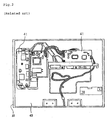
- Fig. 1 illustrates a construction of a related art flat display device
- Fig. 2 illustrates a structure in which a circuit board is fixed in the related art flat display device.
- a display device includes a plastic rear cover 30, a metallic frame 40, a display module 20, and a plastic front cover 10 connected to the rear cover 30.
- the frame 40 is disposed on a rear surface of the display module 20, and a circuit board 41 for controlling an operation of the display module 20 is connected on a rear surface of the frame 40.
- the circuit board 41 is fixed to the frame 40 with a fixing member such as a screw, and the frame 40 supports the circuit board 41.
- the display module 20 displays an image in accordance with a video signal and a control signal outputted from the circuit board 41.
- the related art flat display device undesirably has increased thickness and weight because it uses a thick metallic frame 40. Further, the related art flat display device undesirably requires a complicated assembly process because the circuit board 41 must be fixed to the frame 40 with a fixing member such as a screw.
- the present invention is directed to a display device that substantially obviates one or more problems due to limitations and disadvantages of the
- An object of the present invention is to provide a display device having an improved installation structure for a circuit board thereof, thereby making it possible to greatly reduce the total thickness and weight thereof.
- Another object of the present invention is to provide a display device having an improved installation structure for a circuit board thereof, thereby making it possible to easily install a circuit board thereof on a display module thereof.
- a display device includes a display module for displaying a video image, a circuit board for providing a video signal and a control signal to the display module, and a fixing plate fixed on a rear surface of the display module and having a fixing portion for fixing the circuit board to the fixing plate.
- a display device in another aspect of the present invention, includes a display module for displaying a video image, a circuit board for providing a video signal and a control signal to the display module, and a fixing plate fixed on a rear surface of the display module, the circuit board being inserted into and fixed to the fixing plate through elastic deformation of the fixing plate.
- Fig. 1 illustrates a construction of a related art flat display device
- Fig. 2 illustrates a structure in which a circuit board is fixed in a related art flat display device
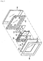
- Fig. 3 is an exploded perspective view of a display device according to the present invention.
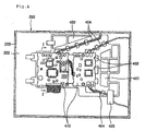
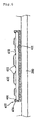
- Figs. 4 and 5 illustrate a structure in which a circuit board is fixed to a fixing plate in a display device according to the present invention.
- Fig. 6 illustrates an alternative structure in which a circuit board is fixed to a fixing plate in a display device according to the present invention.
- Fig. 3 is an exploded perspective view of a display device according to the present invention
- Figs. 4 and 5 illustrate a structure in which a circuit board is fixed to a fixing plate in a display device according to the present invention.
- the inventive display device includes a front cover 100, a rear cover 300 connected to the front cover 100, a display module 200 disposed between the front and rear covers 100 and 300, a fixing plate 400 connected on a rear surface of the display module 200, and a circuit board 410 fixed to the fixing plate 400 and supplying a video signal and a control signal to the display module 200.
- the front and rear covers 100 and 300 constitute a housing of the display device, and may be made of plastic.
- the display module 200 is fixed to the front or rear cover 100 or 300, and displays a video in accordance with inputted video and control signals.
- the display module 200 includes a display panel 201 for displaying video, a mold frame 202 for supporting a rear surface of the display panel 201, a backlight unit (not shown) installed in the mold frame 202 to provide a light source to the display panel 201, and a rectangular frame-type metal chassis 203 for supporting the display panel 201, the mold frame 202 and the backlight unit.
- the mold frame 202 may be made of plastic.
- a fixing plate 400 for fixing at least one circuit board 410 (which provides a video signal and a control signal to the display panel 201) is located on the mold frame 202 of the display module 200.
- the fixing plate 400 is fixed on the mold frame 202 with an insulating adhesive material, such as tape 405 or an insulating adhesive.
- the fixing plate 400 is preferably made of non-conductive material, for example, plastic.
- the fixing plate 400 has a recess 401 formed therein that corresponds to the size and shape of the circuit board 410.
- the circuit board 410 is inserted into and fixed to the recess 401.
- Locking members 402 are formed at the periphery of the recess 401, and lock the circuit board 410 inserted into the recess 401.
- the locking members 402 are elastically deformable and have have elasticity suitable for fixing the inserted circuit board 410 to the fixing plate 400 without using a separate fastening member.
- the circuit board 410 is completely inserted into the fixing plate 400 (specifically, the recess 401), and circuit components 411 such as various ICs (integrated circuits) are mounted on the circuit board 410 in such a way to protrude outside the fixing plate 400.
- circuit components 411 such as various ICs (integrated circuits) are mounted on the circuit board 410 in such a way to protrude outside the fixing plate 400.
- the fixing member may be configured as a deflectable snap-in locking tab 422 formed on the fixing plate 400 so as to secure the circuit board 410 to the fixing plate 400.
- the snap-in locking tab 422 has a hook portion 424 at a distal end thereof with an inclined surface 426. The inclined surface 426 is contacted by the circuit board 410 being installed to the fixing plate 400, and causes the locking tab 422 to deflect outwardly so that the circuit board 410 can be located under and secured by the hook portion 424 of the locking tab 422.
- Fig. 6 shows that the fixing plate 400 may be configured without the recess 401 shown in Fig. 5 for receiving the circuit board 410.
- the fixing plate 400 is preferably formed of non-combustible or low combustible material so as to resist sparks or flames that may be generated at the circuit board 410, and preferably has at least one or more convex beads 403 formed thereon for reinforcing the stiffness thereof. Also, the fixing plate 400 preferably has one or more guide grooves 404 therein for guiding electric wires connected respectively to the display module 200, an external power source, and external electronic devices.
- a porous aluminum shield 500 for preventing the spread of an electromagnetic wave and a flame that may be generated at the circuit board 410 is preferably formed between the display module 200 and the rear cover 300.
- the fixing plate 400 is fixed on a rear surface of the mold frame 202 of the display module 200 with an adhesive material, such as adhesive tape 405. Thereafter, when being pushed into the recess 401 of the fixing plate 400, the circuit board 410 is inserted into the recess 401 by elastically deforming the elastic recess 401, and is then supported and fixed by the elastic recess 401. Thereafter, the shield 500, the front cover 100 and the rear cover 300 are connected with each other, whereby the inventive display device is completely assembled.
- an adhesive material such as adhesive tape 405.
- the present invention fixes the circuit board for driving the display module to the thin light plastic fixing plate, thereby reducing the thickness and weight of the display device. Also, the present invention makes it possible to easily fix the circuit board to the fixing plate, thereby facilitating the assembly of the display device.
Landscapes
- Physics & Mathematics (AREA)
- Nonlinear Science (AREA)
- Mathematical Physics (AREA)
- Chemical & Material Sciences (AREA)
- Crystallography & Structural Chemistry (AREA)
- General Physics & Mathematics (AREA)
- Optics & Photonics (AREA)
- Devices For Indicating Variable Information By Combining Individual Elements (AREA)
Abstract

Description
- The present invention relates to a display device, and more particularly, to a display device having a fixing plate for fixing a circuit board thereto for driving a display module of the display device.
- Flat display devices are used as monitors of desktop computers and also used in various electronic devices such as notebook computers, personal digital assistants (PDA) and portable phones. Examples of such flat display devices include a liquid crystal display (LCD), a plasma display panel (PDP) and a field emission display (FED).
- Fig. 1 illustrates a construction of a related art flat display device, and Fig. 2 illustrates a structure in which a circuit board is fixed in the related art flat display device. Referring to Figs. 1 and 2, a display device includes a plastic
rear cover 30, ametallic frame 40, adisplay module 20, and aplastic front cover 10 connected to therear cover 30. - The
frame 40 is disposed on a rear surface of thedisplay module 20, and acircuit board 41 for controlling an operation of thedisplay module 20 is connected on a rear surface of theframe 40. Thecircuit board 41 is fixed to theframe 40 with a fixing member such as a screw, and theframe 40 supports thecircuit board 41. Thedisplay module 20 displays an image in accordance with a video signal and a control signal outputted from thecircuit board 41. - The related art flat display device undesirably has increased thickness and weight because it uses a thick
metallic frame 40. Further, the related art flat display device undesirably requires a complicated assembly process because thecircuit board 41 must be fixed to theframe 40 with a fixing member such as a screw. - Accordingly, the present invention is directed to a display device that substantially obviates one or more problems due to limitations and disadvantages of the
- An object of the present invention is to provide a display device having an improved installation structure for a circuit board thereof, thereby making it possible to greatly reduce the total thickness and weight thereof.
- Another object of the present invention is to provide a display device having an improved installation structure for a circuit board thereof, thereby making it possible to easily install a circuit board thereof on a display module thereof.
- Additional advantages, objects, and features of the invention will be set forth in part in the description which follows and in part will become apparent to those having ordinary skill in the art upon examination of the following or may be learned from practice of the invention. The objectives and other advantages of the invention may be realized and attained by the structure particularly pointed out in the written description and claims hereof as well as the appended drawings.
- To achieve these objects and other advantages and in accordance with the purpose of the invention, as embodied and broadly described herein, a display device includes a display module for displaying a video image, a circuit board for providing a video signal and a control signal to the display module, and a fixing plate fixed on a rear surface of the display module and having a fixing portion for fixing the circuit board to the fixing plate.
- In another aspect of the present invention, a display device includes a display module for displaying a video image, a circuit board for providing a video signal and a control signal to the display module, and a fixing plate fixed on a rear surface of the display module, the circuit board being inserted into and fixed to the fixing plate through elastic deformation of the fixing plate.
- It is to be understood that both the foregoing general description and the following detailed description of the present invention are exemplary and explanatory and are intended to provide further explanation of the invention as claimed.
- The accompanying drawings, which are included to provide a further understanding of the invention and are incorporated in and constitute a part of this application, illustrate embodiment(s) of the invention and together with the description serve to explain the principle of the invention. In the drawings:
- Fig. 1 illustrates a construction of a related art flat display device;
- Fig. 2 illustrates a structure in which a circuit board is fixed in a related art flat display device;
- Fig. 3 is an exploded perspective view of a display device according to the present invention;
- Figs. 4 and 5 illustrate a structure in which a circuit board is fixed to a fixing plate in a display device according to the present invention; and
- Fig. 6 illustrates an alternative structure in which a circuit board is fixed to a fixing plate in a display device according to the present invention.
- Reference will now be made in detail to the preferred embodiments of the present invention, examples of which are illustrated in the accompanying drawings. Wherever possible, the same reference numbers will be used throughout the drawings to refer to the same or like parts.
- Fig. 3 is an exploded perspective view of a display device according to the present invention, and Figs. 4 and 5 illustrate a structure in which a circuit board is fixed to a fixing plate in a display device according to the present invention.
- Referring to Fig. 3, the inventive display device includes a
front cover 100, arear cover 300 connected to thefront cover 100, adisplay module 200 disposed between the front andrear covers fixing plate 400 connected on a rear surface of thedisplay module 200, and acircuit board 410 fixed to thefixing plate 400 and supplying a video signal and a control signal to thedisplay module 200. The front andrear covers - The
display module 200 is fixed to the front orrear cover display module 200 includes adisplay panel 201 for displaying video, amold frame 202 for supporting a rear surface of thedisplay panel 201, a backlight unit (not shown) installed in themold frame 202 to provide a light source to thedisplay panel 201, and a rectangular frame-type metal chassis 203 for supporting thedisplay panel 201, themold frame 202 and the backlight unit. Themold frame 202 may be made of plastic. - As shown in Figs. 4 and 5, a
fixing plate 400 for fixing at least one circuit board 410 (which provides a video signal and a control signal to the display panel 201) is located on themold frame 202 of thedisplay module 200. Thefixing plate 400 is fixed on themold frame 202 with an insulating adhesive material, such astape 405 or an insulating adhesive. Thefixing plate 400 is preferably made of non-conductive material, for example, plastic. Thefixing plate 400 has arecess 401 formed therein that corresponds to the size and shape of thecircuit board 410. - The
circuit board 410 is inserted into and fixed to therecess 401.Locking members 402 are formed at the periphery of therecess 401, and lock thecircuit board 410 inserted into therecess 401. Thelocking members 402 are elastically deformable and have have elasticity suitable for fixing the insertedcircuit board 410 to thefixing plate 400 without using a separate fastening member. - As shown in Fig. 5, the
circuit board 410 is completely inserted into the fixing plate 400 (specifically, the recess 401), andcircuit components 411 such as various ICs (integrated circuits) are mounted on thecircuit board 410 in such a way to protrude outside thefixing plate 400. - As shown in Fig. 6, the fixing member may be configured as a deflectable snap-in
locking tab 422 formed on thefixing plate 400 so as to secure thecircuit board 410 to thefixing plate 400. More specifically, the snap-inlocking tab 422 has ahook portion 424 at a distal end thereof with an inclined surface 426. The inclined surface 426 is contacted by thecircuit board 410 being installed to thefixing plate 400, and causes thelocking tab 422 to deflect outwardly so that thecircuit board 410 can be located under and secured by thehook portion 424 of thelocking tab 422. In addition, Fig. 6 shows that thefixing plate 400 may be configured without therecess 401 shown in Fig. 5 for receiving thecircuit board 410. - The
fixing plate 400 is preferably formed of non-combustible or low combustible material so as to resist sparks or flames that may be generated at thecircuit board 410, and preferably has at least one or moreconvex beads 403 formed thereon for reinforcing the stiffness thereof. Also, thefixing plate 400 preferably has one ormore guide grooves 404 therein for guiding electric wires connected respectively to thedisplay module 200, an external power source, and external electronic devices. - As shown in Fig. 3, a
porous aluminum shield 500 for preventing the spread of an electromagnetic wave and a flame that may be generated at thecircuit board 410 is preferably formed between thedisplay module 200 and therear cover 300. - In the inventive display device, the
fixing plate 400 is fixed on a rear surface of themold frame 202 of thedisplay module 200 with an adhesive material, such asadhesive tape 405. Thereafter, when being pushed into therecess 401 of thefixing plate 400, thecircuit board 410 is inserted into therecess 401 by elastically deforming theelastic recess 401, and is then supported and fixed by theelastic recess 401. Thereafter, theshield 500, thefront cover 100 and therear cover 300 are connected with each other, whereby the inventive display device is completely assembled. - As stated above, the present invention fixes the circuit board for driving the display module to the thin light plastic fixing plate, thereby reducing the thickness and weight of the display device. Also, the present invention makes it possible to easily fix the circuit board to the fixing plate, thereby facilitating the assembly of the display device.
- It will be apparent to those skilled in the art that various modifications and variations can be made in the present invention. Thus, it is intended that the present invention covers the modifications and variations of this invention provided they come within the scope of the appended claims and their equivalents.
Claims (21)
- A display device comprising:a display module to display a video image;a circuit board to provide a signal to the display module; anda fixing plate fixed on a surface of the display module and having an elastically deformable fixing member to fix the circuit board to the fixing plate.
- The display device according to claim 1, wherein the fixing plate includes a concave recess formed therein corresponding to a shape and size of the circuit board, so that the circuit board may be inserted into the recess and fixed by the fixing member.
- The display device according to claim 2, wherein the fixing member comprises a locking member formed at a periphery of the recess so as to support the circuit board inserted into the recess.
- The display device according to claim 1, wherein the fixing plate is fixed on a rear surface of the display module with an insulating adhesive tape.
- The display device according to claim 1, wherein the fixing plate is fixed on a rear surface of the display module with an insulating adhesive.
- The display device according to claim 1, wherein the fixing plate is non-combustible.
- The display device according to claim 1, wherein the fixing plate is non-conductive.
- The display device according to claim 1, wherein the fixing plate has a concave guide groove for guiding an electric wire connected to the circuit board.
- The display device according to claim 1, wherein the fixing member comprises a deflectable tab formed on the fixing plate so as to secure the circuit board to the fixing plate.
- The display device according to claim 9, wherein the deflectable tab comprises a snap-in locking tab.
- A display device comprising:a display module to display a video image;a circuit board to provide a signal to the display module; anda fixing plate fixed on a surface of the display module, the circuit board being fixed to fixing plate through elastic deformation of the fixing plate.
- The display device according to claim 11, wherein the fixing plate has a recess therein, the circuit board being inserted and seated into the recess.
- The display device according to claim 12, wherein the fixing member comprises a locking member formed at a periphery of the recess so as to support the circuit board inserted into the recess.
- The display device according to claim 11, wherein the fixing plate is fixed on a rear surface of the display module with an insulating adhesive tape.
- The display device according to claim 11, wherein the fixing plate is fixed on a rear surface of the display module with an insulating adhesive.
- The display device according to claim 11, wherein the fixing plate is non-combustible.
- The display device according to claim 11, wherein the fixing plate is non-conductive.
- The display device according to claim 11, wherein the fixing plate has a concave guide groove for guiding an electric wire connected to the circuit board.
- A display device comprising:a display module to display a video image;a circuit board to provide a signal to the display module; anda fixing plate fixed on a surface of the display module to receive the circuit board thereon, the fixing plate being fixed on the surface of the display module with an adhesive material.
- The display device according to claim 19, wherein the adhesive material is an adhesive tape.
- The display device according to claim 19, wherein the adhesive material is an adhesive.
Applications Claiming Priority (1)
| Application Number | Priority Date | Filing Date | Title |
|---|---|---|---|
| KR1020040062075A KR100617116B1 (en) | 2004-08-06 | 2004-08-06 | Video display device |
Publications (1)
| Publication Number | Publication Date |
|---|---|
| EP1624331A1 true EP1624331A1 (en) | 2006-02-08 |
Family
ID=34942458
Family Applications (1)
| Application Number | Title | Priority Date | Filing Date |
|---|---|---|---|
| EP05291401A Withdrawn EP1624331A1 (en) | 2004-08-06 | 2005-06-29 | Flat panel display device |
Country Status (5)
| Country | Link |
|---|---|
| US (1) | US7508655B2 (en) |
| EP (1) | EP1624331A1 (en) |
| KR (1) | KR100617116B1 (en) |
| CN (1) | CN100361004C (en) |
| TW (1) | TWI269582B (en) |
Families Citing this family (30)
| Publication number | Priority date | Publication date | Assignee | Title |
|---|---|---|---|---|
| WO2006098365A1 (en) * | 2005-03-15 | 2006-09-21 | Matsushita Electric Industrial Co., Ltd. | Display device |
| KR100646563B1 (en) * | 2005-07-04 | 2006-11-14 | 삼성에스디아이 주식회사 | Plasma display |
| JP2007279577A (en) | 2006-04-11 | 2007-10-25 | Sony Corp | Electronic equipment |
| JP4725792B2 (en) * | 2006-04-11 | 2011-07-13 | ソニー株式会社 | Electronics |
| JP4191204B2 (en) * | 2006-05-12 | 2008-12-03 | エルピーダメモリ株式会社 | Semiconductor device and manufacturing method thereof |
| KR100741132B1 (en) * | 2006-06-20 | 2007-07-19 | 삼성에스디아이 주식회사 | Plasma display device |
| CN101179911B (en) * | 2006-11-09 | 2010-09-29 | 瀚斯宝丽股份有限公司 | Sealing Mechanism for Flat Panel Display |
| CN101261387B (en) * | 2007-03-07 | 2011-08-24 | 奇美电子股份有限公司 | Backlight module, liquid crystal display device using the backlight module, and assembly method |
| JP5259110B2 (en) * | 2007-03-27 | 2013-08-07 | 三菱電機株式会社 | Display device |
| US7940518B2 (en) * | 2007-04-03 | 2011-05-10 | Pandigital, Inc. | Dual frame electronic display |
| EP2153273B1 (en) * | 2007-06-01 | 2017-05-10 | LG Display Co., Ltd. | Display device |
| WO2009025025A1 (en) * | 2007-08-20 | 2009-02-26 | Mitsubishi Electric Corporation | Display device |
| CN101449899A (en) * | 2007-12-07 | 2009-06-10 | 鸿富锦精密工业(深圳)有限公司 | Digital photo-frame |
| CN101930259A (en) * | 2009-06-25 | 2010-12-29 | 鸿富锦精密工业(深圳)有限公司 | Monitors and Computers |
| KR101710647B1 (en) * | 2009-08-25 | 2017-02-27 | 삼성전자 주식회사 | Display apparatus and portable computer having the same |
| KR101598372B1 (en) * | 2009-09-18 | 2016-02-29 | 엘지디스플레이 주식회사 | Liquid crystal display device |
| CN102542932A (en) * | 2011-01-04 | 2012-07-04 | 康准电子科技(昆山)有限公司 | Display |
| US8654517B2 (en) * | 2011-01-04 | 2014-02-18 | Microsoft Corporation | Structural chassis for a display device |
| WO2012120739A1 (en) * | 2011-03-04 | 2012-09-13 | パナソニック株式会社 | Lighting apparatus |
| JP2012253094A (en) * | 2011-05-31 | 2012-12-20 | Sony Corp | Electronic apparatus |
| CN102243390A (en) * | 2011-07-06 | 2011-11-16 | 深圳市华星光电技术有限公司 | Liquid crystal display device and back plate of backlight module of liquid crystal display device |
| US8861198B1 (en) | 2012-03-27 | 2014-10-14 | Amazon Technologies, Inc. | Device frame having mechanically bonded metal and plastic |
| US8922983B1 (en) * | 2012-03-27 | 2014-12-30 | Amazon Technologies, Inc. | Internal metal support structure for mobile device |
| US8804321B2 (en) * | 2012-05-25 | 2014-08-12 | Steelcase, Inc. | Work and videoconference assembly |
| CN104238173B (en) * | 2014-09-16 | 2017-12-05 | 深圳市华星光电半导体显示技术有限公司 | Flat display devices |
| CN104715681B (en) * | 2015-02-12 | 2017-07-28 | 明基电通有限公司 | For the induction installation and face equipment of the backlight intensity for detecting panel module |
| US9541961B1 (en) | 2015-08-25 | 2017-01-10 | Microsoft Technology Licensing, Llc | Shielding via display chassis |
| US10007302B2 (en) * | 2016-02-15 | 2018-06-26 | Neocoil, Llc | Magnetic resonance imaging compatible mobile computing device |
| KR102730876B1 (en) * | 2019-06-04 | 2024-11-18 | 삼성전자주식회사 | Display apparatus |
| US12200909B2 (en) | 2020-10-01 | 2025-01-14 | Nvidia Corporation | Rack form-factor reservoir for datacenter cooling systems |
Citations (4)
| Publication number | Priority date | Publication date | Assignee | Title |
|---|---|---|---|---|
| DE3313080A1 (en) * | 1983-04-12 | 1984-10-18 | Brown, Boveri & Cie Ag, 6800 Mannheim | Device for contacting a display unit to a liquid crystal layer |
| US4727285A (en) * | 1984-07-06 | 1988-02-23 | Sharp Kabushiki Kaisha | Display device and printed circuit board |
| US20010000763A1 (en) * | 1998-08-18 | 2001-05-03 | Seiko Epson Corporation | Circuit board connecting structure, electro-optical device, electronic apparatus provided with the same, and manufacturing method for electro-optical device |
| WO2004008233A1 (en) * | 2002-07-11 | 2004-01-22 | Diehl Ako Stiftung & Co. Kg | Backlit liquid crystal display, particularly for use as a display module behind the operating panel of a large household appliance |
Family Cites Families (20)
| Publication number | Priority date | Publication date | Assignee | Title |
|---|---|---|---|---|
| US5268816A (en) * | 1982-09-28 | 1993-12-07 | Lexmark International, Inc. | Movable display screen for a computer |
| US5293262A (en) * | 1988-03-15 | 1994-03-08 | Mitsubishi Denki Kabushiki Kaisha | Liquid crystal display device having heat-insulating members and driving circuit boards attached to rear edges of light box |
| JPH05203923A (en) * | 1991-10-31 | 1993-08-13 | Matsushita Electric Ind Co Ltd | Liquid crystal display board holding device |
| US5422751A (en) * | 1992-10-14 | 1995-06-06 | Apple Computer, Inc. | Liquid crystal display assembly employing front bezel, frame holding liquid crystal cell attached to bezel, and light source and back plate attached to bezel |
| JP2885693B2 (en) * | 1996-04-23 | 1999-04-26 | 静岡日本電気株式会社 | LCD holding structure for small electronic devices |
| JP2000066231A (en) * | 1998-08-25 | 2000-03-03 | Seiko Epson Corp | Liquid crystal display |
| JP3473445B2 (en) * | 1998-09-30 | 2003-12-02 | 三菱電機株式会社 | Screen manufacturing method using flat display panel |
| JP2000181362A (en) * | 1998-12-17 | 2000-06-30 | Alps Electric Co Ltd | Liquid crystal display device |
| JP3708779B2 (en) * | 1999-03-29 | 2005-10-19 | セイコーエプソン株式会社 | Liquid crystal display device, flat display device, and electronic apparatus equipped with the same |
| KR200218685Y1 (en) * | 1999-06-28 | 2001-04-02 | 김순택 | LCD assembly |
| JP2001108968A (en) * | 1999-10-01 | 2001-04-20 | Matsushita Electric Ind Co Ltd | Electronic equipment with liquid crystal display |
| JP3301540B2 (en) * | 1999-12-09 | 2002-07-15 | 日本精機株式会社 | Liquid crystal display |
| JP2002196312A (en) * | 2000-12-25 | 2002-07-12 | Hitachi Ltd | Liquid crystal display |
| KR100793729B1 (en) * | 2001-09-27 | 2008-01-10 | 삼성전자주식회사 | LCD Display |
| TW583529B (en) * | 2001-11-15 | 2004-04-11 | Wistron Corp | Liquid crystal display computer with a removable device frame |
| JP2003345265A (en) * | 2002-05-27 | 2003-12-03 | Matsushita Electric Ind Co Ltd | Plasma display device |
| KR100471064B1 (en) * | 2002-06-11 | 2005-03-10 | 삼성전자주식회사 | Displaying apparatus |
| JP3757923B2 (en) * | 2002-09-20 | 2006-03-22 | セイコーエプソン株式会社 | Electronics |
| JP4551633B2 (en) * | 2003-07-02 | 2010-09-29 | パナソニック株式会社 | Flat panel display |
| US7173678B2 (en) * | 2004-06-25 | 2007-02-06 | Northrop Grumman Corporation | Non-ruggedized COTS display packaging for severe environment applications |
-
2004
- 2004-08-06 KR KR1020040062075A patent/KR100617116B1/en not_active Expired - Lifetime
-
2005
- 2005-06-16 US US11/153,614 patent/US7508655B2/en active Active
- 2005-06-20 CN CNB2005100783750A patent/CN100361004C/en not_active Expired - Fee Related
- 2005-06-29 EP EP05291401A patent/EP1624331A1/en not_active Withdrawn
- 2005-07-26 TW TW094125230A patent/TWI269582B/en not_active IP Right Cessation
Patent Citations (4)
| Publication number | Priority date | Publication date | Assignee | Title |
|---|---|---|---|---|
| DE3313080A1 (en) * | 1983-04-12 | 1984-10-18 | Brown, Boveri & Cie Ag, 6800 Mannheim | Device for contacting a display unit to a liquid crystal layer |
| US4727285A (en) * | 1984-07-06 | 1988-02-23 | Sharp Kabushiki Kaisha | Display device and printed circuit board |
| US20010000763A1 (en) * | 1998-08-18 | 2001-05-03 | Seiko Epson Corporation | Circuit board connecting structure, electro-optical device, electronic apparatus provided with the same, and manufacturing method for electro-optical device |
| WO2004008233A1 (en) * | 2002-07-11 | 2004-01-22 | Diehl Ako Stiftung & Co. Kg | Backlit liquid crystal display, particularly for use as a display module behind the operating panel of a large household appliance |
Also Published As
| Publication number | Publication date |
|---|---|
| KR20060013203A (en) | 2006-02-09 |
| CN1731481A (en) | 2006-02-08 |
| US7508655B2 (en) | 2009-03-24 |
| KR100617116B1 (en) | 2006-08-31 |
| TWI269582B (en) | 2006-12-21 |
| US20060028790A1 (en) | 2006-02-09 |
| CN100361004C (en) | 2008-01-09 |
| TW200607343A (en) | 2006-02-16 |
Similar Documents
| Publication | Publication Date | Title |
|---|---|---|
| US7508655B2 (en) | Display device | |
| KR100487435B1 (en) | liquid crystal display device module having a mounting frame combination structure | |
| CN1257426C (en) | Structure for mounting flat-panel displays | |
| US7623195B2 (en) | Structure for assembling lamp wires for backlight assembly into liquid crystal display module | |
| US6891718B2 (en) | Structure for assembling flat display | |
| CN1466025A (en) | Computer system with replaceable liquid crystal display | |
| US20040066473A1 (en) | Display device | |
| US6618240B1 (en) | Computer having a flat panel display | |
| KR100487438B1 (en) | Liquid Crystal Display Device | |
| US20060187374A1 (en) | Backlight assembly | |
| US20080106670A1 (en) | Backlight module having a fastening structure and liquid crystal display using the same | |
| JP4694789B2 (en) | Panel member unit, electronic device and mounting member | |
| KR100319202B1 (en) | Liquid crystal display device | |
| US7474364B2 (en) | Structure for mounting an inverter | |
| KR20060082471A (en) | Liquid crystal display | |
| JP4572593B2 (en) | Liquid crystal display | |
| JP4695228B2 (en) | Panel member unit, electronic device and mounting member | |
| KR20050060821A (en) | Liquid crystal display structure for a car audio | |
| TW556139B (en) | Liquid crystal display unit and its housing component | |
| KR100698123B1 (en) | Socket Fixing Structure of Image Display Device | |
| KR0114102Y1 (en) | Pcb fixing device in monitor | |
| KR20060061869A (en) | Liquid crystal display with bending protection against external shock | |
| KR20060016945A (en) | Video display shield | |
| KR20070038200A (en) | LCD Display |
Legal Events
| Date | Code | Title | Description |
|---|---|---|---|
| PUAI | Public reference made under article 153(3) epc to a published international application that has entered the european phase |
Free format text: ORIGINAL CODE: 0009012 |
|
| AK | Designated contracting states |
Kind code of ref document: A1 Designated state(s): AT BE BG CH CY CZ DE DK EE ES FI FR GB GR HU IE IS IT LI LT LU MC NL PL PT RO SE SI SK TR |
|
| AX | Request for extension of the european patent |
Extension state: AL BA HR LV MK YU |
|
| 17P | Request for examination filed |
Effective date: 20060704 |
|
| AKX | Designation fees paid |
Designated state(s): DE FR GB |
|
| 17Q | First examination report despatched |
Effective date: 20090225 |
|
| STAA | Information on the status of an ep patent application or granted ep patent |
Free format text: STATUS: THE APPLICATION IS DEEMED TO BE WITHDRAWN |
|
| 18D | Application deemed to be withdrawn |
Effective date: 20090708 |