EP1622267A1 - Line termination circuit - Google Patents
Line termination circuit Download PDFInfo
- Publication number
- EP1622267A1 EP1622267A1 EP04025776A EP04025776A EP1622267A1 EP 1622267 A1 EP1622267 A1 EP 1622267A1 EP 04025776 A EP04025776 A EP 04025776A EP 04025776 A EP04025776 A EP 04025776A EP 1622267 A1 EP1622267 A1 EP 1622267A1
- Authority
- EP
- European Patent Office
- Prior art keywords
- resistance
- transmission line
- mos transistor
- channel type
- line
- Prior art date
- Legal status (The legal status is an assumption and is not a legal conclusion. Google has not performed a legal analysis and makes no representation as to the accuracy of the status listed.)
- Granted
Links
Images


Classifications
-
- H—ELECTRICITY
- H03—ELECTRONIC CIRCUITRY
- H03K—PULSE TECHNIQUE
- H03K19/00—Logic circuits, i.e. having at least two inputs acting on one output; Inverting circuits
- H03K19/0005—Modifications of input or output impedance
-
- H—ELECTRICITY
- H04—ELECTRIC COMMUNICATION TECHNIQUE
- H04L—TRANSMISSION OF DIGITAL INFORMATION, e.g. TELEGRAPHIC COMMUNICATION
- H04L25/00—Baseband systems
- H04L25/02—Details ; arrangements for supplying electrical power along data transmission lines
- H04L25/0264—Arrangements for coupling to transmission lines
- H04L25/0298—Arrangement for terminating transmission lines
Definitions
- the present invention relates to a signal transmission technology, more particularly to a technology for a termination circuit for matching a plurality of segments of impedance of a transmission line.
- DDR2 double data rate 2
- JEDEC Joint Electron Device Engineering Council
- the termination circuit on the controller side in a DDR2 interface is activated when a controller receives data, and it is inactivated when the controller transmits data. It is stipulated that the matched impedance of a transmission line should be 75ohms. Therefore, if a controller and memory are connected 1 to 1, the termination resistance value is made to be 75ohms. However, if a controller and memory are connected 1 to 2, the terminal resistance value can be switched to 150ohms. Furthermore, the termination circuit is required to form Thevenin termination.
- FIG. 1 One configuration of a termination circuit for meeting such a requirement is shown in Fig. 1.
- resistors 101a, 101b, 101c and 101d are disposed in each data transmission line leading to memory 200 in a controller 100.
- the resistors 101a and 101c are connected in parallel between a transmission line and a power supply line, and the resistors 101b and 101d are connected in parallel between the transmission line and a ground line.
- the resistance value of each of the resistors 101a, 101b, 101c and 101d is 300ohms. Therefore, this circuit forms Thevenin termination and its termination resistance value becomes 75ohms.
- FIG. 2 One detailed configuration of the termination circuit on the semiconductor substrate in a semiconductor device is shown in Fig. 2.
- P-channel type metal oxide semiconductor (MOS) transistors 111a and 111c provided between a transmission line 102 and a power supply line 103 correspond to the resistors 101a and 101c, respectively
- N-channel type MOS transistors 111b and 111d correspond to the resistors 101b and 101c, respectively.
- P-channel type MOS transistors 111e and N-channel type MOS transistor 111f are used to connect/ disconnect the P-channel type MOS transistor 111a and 111c and the N-channel type MOS transistors 111b and 111d to/from the transmission line 102, and are formed in such a way that the resistance value (so-called "on resistance") between the drain terminal and the source terminal can be made sufficiently low when operating them in a saturation region.
- the P-channel type MOS transistors (hereinafter called “P-type transistor”) 111a and 111c are switched on if the signal level of its gate terminal is L (low level), and the N-channel type MOS transistors (hereinafter called “N-type transistor”) 111b and 111d are switched on if the signal level of its gate terminal is H (high level) .
- its gate width is formed in such a way that the on resistance of each of the P-type transistors 111a and 111c and the N-type transistors 111b and 111d can become 300ohms. Therefore, if the respective signal levels of the gate terminals of these transistors 111a, 111b, 111c and 111d are all controlled so as to be switched on, this circuit forms Thevenin termination and its termination resistance value becomes 75ohms.
- the termination circuit shown in Fig. 2 utilizes the respective on resistance of transistors 111a, 111b, 111c and 111d, the termination circuit has the following problems.
- the terminal resistance value varies depending on a transmission signal if viewed from the transmission line 102 side, and the signal transmission quality of the transmission line 102 degrades.
- Japanese Patent Application No. 2002-344300 discloses a technology for suppressing the dispersion of termination resistance values by enabling a transistor used to operate as a termination resistor in a non-saturation region and also controlling the gate terminal voltage of a transistor based on a reference resistance to obtain proper on resistance.
- this technology requires an analog circuit for generating gate terminal voltage for proper on resistance in a transistor based on the reference resistance.
- a termination circuit in one aspect of the present invention terminates a transmission line.
- the termination circuit comprises a resistance unit which is formed by connecting a P-channel type metal oxide semiconductor (MOS) transistor and an N-channel type MOS transistor in parallel, and Thevenin termination is formed by providing this resistance unit between the transmission line and the power line and between the transmission line and the ground line.
- MOS metal oxide semiconductor
- the potential range of the transmission line in which the respective resistance characteristics of a P-channel type MOS transistor and an N-channel type MOS transistor both degrade is very narrow. Therefore, if the connection of both the transistors is used as termination resistance, as described above, the degradation of the signal transmission quality of the transmission line can be suppressed more, compared with a case where both the transistors are used without being combined by their parallel connection.
- the P-channel type and the N-channel type MOS transistors can also be formed in such a way that the sum of the respective gate threshold voltage of the P-channel type and N-channel type MOS transistors composing the above-mentioned resistance unit can drop below the power supply voltage of the above-mentioned circuit.
- the resistance unit is formed in such a way as to meet the above-mentioned requirements, the respective resistance characteristics of the parallel connection of P-channel type and N-channel type MOS transistors at the time of on operation both do not always degrade simultaneously. Therefore, the change of the resistance characteristic of the resistance unit due to the signal level of the transmission line can be far more sufficiently suppressed.
- the above-mentioned termination circuit of the present invention can also further insert a plurality of resistance units between the above-mentioned transmission line and the above-mentioned power line and between the transmission line and the above-mentioned ground line and further comprise a control unit for individually controlling each of the resistance units to switch the on/off operation of the P-channel type and the N-channel type MOS transistors composing the resistance unit.
- the transmission line can be more appropriately matched.
- serial connection between the above-mentioned parallel connection of the plurality of resistance units and a resistance device can also be provided between the above-mentioned transmission line and the above-mentioned power supply line and between the transmission line and the above-mentioned ground line.
- a poly-silicon resistor or the like can be used for the resistance device.
- the gate width of a MOS transistor composing the above-mentioned resistance unit can also be different from the respective gate width of the other MOS transistors composing the resistance unit.
- the resistance value of the resistance unit can be adjusted over a wider range or in finer steps, and accordingly, the transmission line can be more appropriately matched.
- the present invention includes a semiconductor device in which the above-mentioned termination circuit of the present invention is formed, and also includes an electronic device provided with this semiconductor device.
- the matching characteristic of a termination circuit using a transistor as a termination resistor can be improved.
- Fig. 3 shows the configuration of the termination circuit for implementing the present invention.
- the same reference numerals are attached to the same lines as in Fig. 2.
- this termination circuit is formed on a single semiconductor substrate in a semiconductor device 1.
- This semiconductor device 1 is, for example, a central processing unit (CPU) , and is provided for an electronic device 2, such as a computer or the like.
- the termination circuit shown in Fig. 3 comprises a termination unit 10 for forming Thevenin termination and a control unit 40 for controlling both the switching of activation/inactivation of the terminal circuit and switching of a termination resistance value.
- the termination unit 10 comprises both a first termination unit 10a and a second termination unit 10b for each transmission line 102. Although the circuit configuration of the first termination unit is described below, the second termination unit 10b also has the same circuit configuration.
- a pair of a P-type transistor 11a and an N-type transistor 11b is connected in parallel between the drain terminal and the source terminal to form a resistance unit.
- a control line 41a individually led from the control unit 40 is connected both to the gate terminal of the P-type transistor 11a and to the input of an inverter 20a.
- the output of this inverter 20a is connected to the gate terminal of the N-type transistor 11b. Therefore, if the signal level of the control line 41a becomes L, the gate terminal level of the P-type transistor 11a becomes L, and the gate terminal level of the N-type transistor 11b becomes H by the operation of the inverter 20a. Therefore, the P-type transistor 11a and the N-type transistor 11b are both switched on simultaneously.
- the resistance characteristic (proportional relationship between voltage change ⁇ Vds and current change ⁇ Ids between the drain terminal and the source terminal) of the P-type transistor 11a at the time of on operation degrades. If the gate threshold voltage of the N-type transistor 11b and voltage between the gate terminal and the source terminal at the time of on operation (that is, voltage VDD of the power supply line 103) are expressed by VthN and Vgs, respectively, the resistance characteristic at the time of on operation degrades when the potential of the transmission line 102 exceeds Vgs-VthN.
- the potential range of the transmission line in which the respective resistance characteristics of the P-type transistor 11a and the N-type transistor 11b both degrade is very narrow. Therefore, if the connection of both the transistors is used as termination resistance, as described above, the degradation of the signal transmission quality of the transmission line can be suppressed more, compared with a case where both the transistors are used without being combined by their parallel connection.
- the P-type transistor 11a and the N-type transistor 11b are formed in such a way that the relationship between the gate threshold voltage VthP of the P-type transistor 11a and the gate threshold voltage VthN of the N-type transistor 11b, which are a pair of transistors composing the resistance unit, satisfies the following equation, the far better signal transmission quality of the transmission line 102 can be obtained.
- Vgs is voltage between the gate terminal and the source terminal (that is, potential VDD of the power supply line 103) at the time of on operation.
- the signal level of the transmission line 102 is lower than the potential VDD of the power supply line 103.
- the resistance unit is formed in such a way as to satisfy the above-mentioned equation, the respective resistance characteristics of the parallel-connected P-type transistor 11a and N-type transistor 11b at the time of on operation both do not always degrade simultaneously, regardless of the signal level of the transmission line 102. Therefore, the change of the resistance characteristic of the resistance unit due to the signal level of the transmission line 102 can be suppressed far more sufficiently.
- equation (1) canbe satisfied if the P-type transistor 11a and the N-type transistor 11b are formed in such a way that the sum of the respective gate threshold voltage of the P-type transistor 11a and the N-type transistor 11b that compose the resistance unit can become lower than the power supply voltage of the circuit shown in Fig. 3.
- transistors 12a, 12b, ..., 1na, 1nb and inverters 20b, .., 20n, respectively are also connected similarly, and furthermore, the respective drain terminals and source terminals of transistors 11a and 11b, 12a and 12b, ..., 1na and 1nb, which are these n pairs in total of the respective resistance units, are connected in parallel.
- a control line 42a individually led from the control unit 40 is connected both to the gate terminal of the N-type transistor 11d and to the input of an inverter 30a.
- the output of this inverter 30a is connected to the gate terminal of the P-type transistor 11c. Therefore, if the signal level of the control line 42a becomes H, the gate terminal level of the N-type transistor 11d becomes H, and the gate terminal level of the P-type transistor 11c becomes L by the operation of the inverter 30a. Therefore, the P-type transistor 11c and the N-type transistor 11d are both switched on simultaneously.
- transistors 12c, 12d, ..., 1nc, 1nd and inverters 30b, ..., 30n, respectively are also connected similarly, and furthermore, the respective drain terminals and source terminals of transistors 11c and 11d, 12c and 12d, ..., 1nc and 1nd, which are these n pairs in total of the respective resistance units, are connected in parallel.
- the respective drain terminals of transistors 11a and 11b, 12a and 12b, ..., 1na and 1nb are connected to the power supply line 103, and their respective source terminals are connected to the transmission line 102 through a poly-silicon resistor 31.
- the respective drain terminals of transistors 11c, 11d, 12c, 12d, ..., 1nc, 1nd are connected to the transmission line 102 through a poly-silicon resistor 32, and their respective source terminals are connected to the ground line 104.
- control unit 40 for switching the on/off operation of each transistor in the termination unit is described.
- a power supply side resistance accuracy adjustment control signal line 51 is connected to one of the two inputs of each OR circuits 41, and a ground side resistance accuracy adjustment control signal line 52 is connected to one of the two inputs of each AND circuits 42.
- An on/off signal line 53 is connected both to the other input of each the AND circuits 42 and to the input of an inverter 43. The output of the inverter 43 is connected to the other input of each the OR circuits 41.
- transistors 11a and 11b, 12a and 12b, ..., 1na and 1nb, 11c and 11d, 12c and 12d, ..., 1nc and 1nd are all always switched off. Namely, in this case, transistors 11a, 11b, 12a, 12b, ..., 1na, 1nb, 11c, 11d, 12c, 12d, ..., 1nc, 1nd, which are termination resistors, are all severed from the transmission line 102.
- these transistors provided for the second termination unit 10b whose circuit configuration is the same as the first termination unit 10a, are also severed from the transmission line 102. Therefore, in this case, the termination circuit shown in Fig. 3 is always inactive against the transmission line 102.
- Each outputs of the OR circuits 41 is connected to one of the two inputs of each OR circuits 45, and each outputs of the AND circuits 42 is connected to one of the two inputs of each AND circuits 46.
- a termination resistance value selection signal line 54 is connected both to one of the two inputs of each the AND circuits 46 and to the input of an inverter 44.
- the output of the inverter 44 is connected to the other input of each the OR circuits 45.
- the transistors provided for the second termination unit 10b of the termination unit 10 are all severed from the transmission line 102. Therefore, in this case, the second termination unit 10b always becomes inactive, and only the first termination unit 10a gives influences to the transmission line 102.
- the level of the termination resistance value selection line 54 is H, as long as not specified otherwise.
- the first termination unit 10a can be regarded as the resistance 101a and 101b shown in Fig. 2, it is clear that the second termination unit 10b with the same configuration as the first termination unit 10a can be regarded as the resistance 101c and 101d.
- the termination unit 10 shown in Fig. 3 forms the resistance termination circuit with the Thevenin termination shown in Fig. 2.
- the termination resistance value of the termination circuit shown in Fig. 3 can be switched while maintaining Thevenin termination.
- the termination circuit shown in Fig. 3 can also be made inactive against the transmission line 102.
- each resistance value composing Thevenin termination can be adjusted.
- the poly-silicon resistor 31 or 32 can also be deleted and short-circuited.
- the parallel connections of the transistors 11a and 11b, 12a, and 12b, ..., 1na and 1nb can also directly inserted between the transmission line 102 and the ground line 104.
- the parallel connections of the transistors 11c and 11d, 12c and 12d, ..., 1nc and 1nd can be inserted between the transmission line 102 and the ground line 104.
- a better resistance characteristic can be obtained by using a pure resistance device, such as a poly-silicon resistor than by utilizing the on resistance of a transistor. Therefore, the configuration shown in Fig. 3 using poly-silicon resistors 31 and 32 can provide the transmission line 102 with better signal transmission quality.
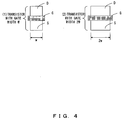
- Fig. 4 shows the respective structures of MOS transistors each with different gate width.
- (1) and (2) show the structures of a transistor with gate width w and a transistor with gate width 2w (twice of that of (1)), respectively.
- the on resistance value of a MOS transistor is inversely proportional to gate width. Therefore, in Fig. 4, transistor (1) provides an on resistance value twice that of transistor (2). In other words, if as shown in Fig. 3, each pair of transistors composing the resistance unit is different, each resistance value composing Thevenin termination can be adjusted over a range wider or in finer steps than in a case where each pair of transistors is the same, by switching the respective signal levels of the power supply side resistance accuracy adjustment control signal line 51 and the ground side resistance accuracy adjustment control signal line 52.
Landscapes
- Engineering & Computer Science (AREA)
- Power Engineering (AREA)
- Computer Hardware Design (AREA)
- Computing Systems (AREA)
- General Engineering & Computer Science (AREA)
- Mathematical Physics (AREA)
- Physics & Mathematics (AREA)
- Computer Networks & Wireless Communication (AREA)
- Signal Processing (AREA)
- Logic Circuits (AREA)
- Dc Digital Transmission (AREA)
- Dram (AREA)
- Semiconductor Integrated Circuits (AREA)
- Networks Using Active Elements (AREA)
Abstract
Description
- The present invention relates to a signal transmission technology, more particularly to a technology for a termination circuit for matching a plurality of segments of impedance of a transmission line.
- In a memory interface based on double data rate 2 (DDR2) rating stipulated by Joint Electron Device Engineering Council (JEDEC), it is required that a termination circuit should be provided on the controller side of memory.
- It is required that the termination circuit on the controller side in a DDR2 interface is activated when a controller receives data, and it is inactivated when the controller transmits data. It is stipulated that the matched impedance of a transmission line should be 75ohms. Therefore, if a controller and memory are connected 1 to 1, the termination resistance value is made to be 75ohms. However, if a controller and memory are connected 1 to 2, the terminal resistance value can be switched to 150ohms. Furthermore, the termination circuit is required to form Thevenin termination.
- One configuration of a termination circuit for meeting such a requirement is shown in Fig. 1.
- In Fig. 1, four
resistors memory 200 in acontroller 100. Theresistors resistors resistors - In this case, if one resistor between the transmission line and the power supply line (for example,
resistor 101c) and one resistor between the transmission line and the ground line (for example,resistor 101d) of the fourresistors resistors resistors - One detailed configuration of the termination circuit on the semiconductor substrate in a semiconductor device is shown in Fig. 2. In Fig. 2, P-channel type metal oxide semiconductor (MOS)
transistors transmission line 102 and apower supply line 103 correspond to theresistors type MOS transistors resistors - P-channel
type MOS transistors 111e and N-channeltype MOS transistor 111f are used to connect/ disconnect the P-channeltype MOS transistor type MOS transistors transmission line 102, and are formed in such a way that the resistance value (so-called "on resistance") between the drain terminal and the source terminal can be made sufficiently low when operating them in a saturation region. - The P-channel type MOS transistors (hereinafter called "P-type transistor") 111a and 111c are switched on if the signal level of its gate terminal is L (low level), and the N-channel type MOS transistors (hereinafter called "N-type transistor") 111b and 111d are switched on if the signal level of its gate terminal is H (high level) . In this case, its gate width is formed in such a way that the on resistance of each of the P-
type transistors type transistors transistors - In this case, if one of the P-
type transistors type transistor 111c) and one of the N-type transistors type transistor 111d) are controlled so as to be switched off, its terminal resistance value becomes 150ohms while the Thevenin termination are maintained by the remaining transistors (for example, P-type transistor 111a and N-type transistor 111b). Furthermore, if the signal level of each of the gate terminals of the P-type transistor 111e and the N-type transistor 111f is controlled so as to be switched off, the termination circuit is inactivated. - Since the termination circuit shown in Fig. 2 utilizes the respective on resistance of
transistors - (1) If the gate threshold voltage of each of the P-
type transistors transmission line 102 drops below the VthP, and the resistance value between thetransmission line 102 and thepower supply line 103 exceeds a target value. - (2) If the gate threshold voltage of each of the N-
type transistors transmission line 102 exceeds Vgs-VthN, and the resistance value between thetransmission line 102 and theground line 104 exceeds a target value. - Therefore, the terminal resistance value varies depending on a transmission signal if viewed from the
transmission line 102 side, and the signal transmission quality of thetransmission line 102 degrades. - For this problem, for example, Japanese Patent Application No. 2002-344300 discloses a technology for suppressing the dispersion of termination resistance values by enabling a transistor used to operate as a termination resistor in a non-saturation region and also controlling the gate terminal voltage of a transistor based on a reference resistance to obtain proper on resistance.
- However, this technology requires an analog circuit for generating gate terminal voltage for proper on resistance in a transistor based on the reference resistance.
- For example, in the termination circuit of a memory interface, a lot of transistors must be provided as resistors since there are a lot of transmission lines. However, it is often difficult in connection with other circuits to unify a plurality of wiring layouts to the gate terminal of each transistor. Therefore, in the technology disclosed in the Japanese Patent Application No. 2002-344300, voltage to be supplied to the gate terminal cannot be unified among transistors due to these different wiring layouts. As a result, the on operation resistance values cannot be unified, and the transmission line cannot always be sufficiently matched.
- It is an object of the present invention to improve the matching characteristic of a termination circuit using a transistor as a termination resistor.
- A termination circuit in one aspect of the present invention terminates a transmission line. The termination circuit comprises a resistance unit which is formed by connecting a P-channel type metal oxide semiconductor (MOS) transistor and an N-channel type MOS transistor in parallel, and Thevenin termination is formed by providing this resistance unit between the transmission line and the power line and between the transmission line and the ground line.
- The potential range of the transmission line in which the respective resistance characteristics of a P-channel type MOS transistor and an N-channel type MOS transistor both degrade is very narrow. Therefore, if the connection of both the transistors is used as termination resistance, as described above, the degradation of the signal transmission quality of the transmission line can be suppressed more, compared with a case where both the transistors are used without being combined by their parallel connection.
- In the above-mentioned termination circuit of the present invention, the P-channel type and the N-channel type MOS transistors can also be formed in such a way that the sum of the respective gate threshold voltage of the P-channel type and N-channel type MOS transistors composing the above-mentioned resistance unit can drop below the power supply voltage of the above-mentioned circuit.
- As long as the resistance unit is formed in such a way as to meet the above-mentioned requirements, the respective resistance characteristics of the parallel connection of P-channel type and N-channel type MOS transistors at the time of on operation both do not always degrade simultaneously. Therefore, the change of the resistance characteristic of the resistance unit due to the signal level of the transmission line can be far more sufficiently suppressed.
- The above-mentioned termination circuit of the present invention can also further insert a plurality of resistance units between the above-mentioned transmission line and the above-mentioned power line and between the transmission line and the above-mentioned ground line and further comprise a control unit for individually controlling each of the resistance units to switch the on/off operation of the P-channel type and the N-channel type MOS transistors composing the resistance unit.
- According to this configuration, since the resistance value of each resistance unit can be adjusted, the transmission line can be more appropriately matched.
- In this case, the serial connection between the above-mentioned parallel connection of the plurality of resistance units and a resistance device can also be provided between the above-mentioned transmission line and the above-mentioned power supply line and between the transmission line and the above-mentioned ground line.
- In this case, for the resistance device, a poly-silicon resistor or the like can be used.
- According to this configuration, since a resistance device with a resistance characteristic better than the resistance unit is inserted, the change of the resistance characteristic of the resistance unit due to the signal level of the transmission line can be suppressed far more sufficiently.
- The gate width of a MOS transistor composing the above-mentioned resistance unit can also be different from the respective gate width of the other MOS transistors composing the resistance unit.
- According to this configuration, the resistance value of the resistance unit can be adjusted over a wider range or in finer steps, and accordingly, the transmission line can be more appropriately matched.
- The present invention includes a semiconductor device in which the above-mentioned termination circuit of the present invention is formed, and also includes an electronic device provided with this semiconductor device.
- As described above, according to the present invention, the matching characteristic of a termination circuit using a transistor as a termination resistor can be improved.
- The present invention will be more apparent from the following detailed description when the accompanying drawings are referenced, in which
- Fig. 1 shows one configuration of the termination circuit;
- Fig. 2 shows the one detailed configuration on a semiconductor device of the termination circuit shown in Fig. 1;
- Fig. 3 shows the configuration of the termination circuit for implementing the present invention; and
- Fig. 4 shows the typical structures of MOS transistors each with different gate width.
- The preferred embodiments of the present invention are described below with reference to the drawings.
- Fig. 3 shows the configuration of the termination circuit for implementing the present invention. In Fig. 3, the same reference numerals are attached to the same lines as in Fig. 2.
- In this preferred embodiment, this termination circuit is formed on a single semiconductor substrate in a
semiconductor device 1. Thissemiconductor device 1 is, for example, a central processing unit (CPU) , and is provided for anelectronic device 2, such as a computer or the like. - The termination circuit shown in Fig. 3 comprises a
termination unit 10 for forming Thevenin termination and acontrol unit 40 for controlling both the switching of activation/inactivation of the terminal circuit and switching of a termination resistance value. - The
termination unit 10 comprises both afirst termination unit 10a and asecond termination unit 10b for eachtransmission line 102. Although the circuit configuration of the first termination unit is described below, thesecond termination unit 10b also has the same circuit configuration. - A pair of a P-
type transistor 11a and an N-type transistor 11b is connected in parallel between the drain terminal and the source terminal to form a resistance unit. Acontrol line 41a individually led from thecontrol unit 40 is connected both to the gate terminal of the P-type transistor 11a and to the input of aninverter 20a. The output of thisinverter 20a is connected to the gate terminal of the N-type transistor 11b. Therefore, if the signal level of thecontrol line 41a becomes L, the gate terminal level of the P-type transistor 11a becomes L, and the gate terminal level of the N-type transistor 11b becomes H by the operation of theinverter 20a. Therefore, the P-type transistor 11a and the N-type transistor 11b are both switched on simultaneously. - As described above, if the potential of the
transmission line 102 drops below the gate threshold voltage VthP, the resistance characteristic (proportional relationship between voltage change ΔVds and current change ΔIds between the drain terminal and the source terminal) of the P-type transistor 11a at the time of on operation degrades. If the gate threshold voltage of the N-type transistor 11b and voltage between the gate terminal and the source terminal at the time of on operation (that is, voltage VDD of the power supply line 103) are expressed by VthN and Vgs, respectively, the resistance characteristic at the time of on operation degrades when the potential of thetransmission line 102 exceeds Vgs-VthN. However, the potential range of the transmission line in which the respective resistance characteristics of the P-type transistor 11a and the N-type transistor 11b both degrade is very narrow. Therefore, if the connection of both the transistors is used as termination resistance, as described above, the degradation of the signal transmission quality of the transmission line can be suppressed more, compared with a case where both the transistors are used without being combined by their parallel connection. - The P-
type transistor 11a and the N-type transistor 11b are formed in such a way that the relationship between the gate threshold voltage VthP of the P-type transistor 11a and the gate threshold voltage VthN of the N-type transistor 11b, which are a pair of transistors composing the resistance unit, satisfies the following equation, the far better signal transmission quality of thetransmission line 102 can be obtained.
- In the above-mentioned equation (1), Vgs is voltage between the gate terminal and the source terminal (that is, potential VDD of the power supply line 103) at the time of on operation. In this case, the signal level of the
transmission line 102 is lower than the potential VDD of thepower supply line 103. - If the resistance unit is formed in such a way as to satisfy the above-mentioned equation, the respective resistance characteristics of the parallel-connected P-
type transistor 11a and N-type transistor 11b at the time of on operation both do not always degrade simultaneously, regardless of the signal level of thetransmission line 102. Therefore, the change of the resistance characteristic of the resistance unit due to the signal level of thetransmission line 102 can be suppressed far more sufficiently. - By transforming equation (1), the following equation (2) can be obtained.

- Specifically, equation (1) canbe satisfied if the P-
type transistor 11a and the N-type transistor 11b are formed in such a way that the sum of the respective gate threshold voltage of the P-type transistor 11a and the N-type transistor 11b that compose the resistance unit can become lower than the power supply voltage of the circuit shown in Fig. 3. - Other pairs of
transistors inverters 20b, .., 20n, respectively, are also connected similarly, and furthermore, the respective drain terminals and source terminals oftransistors - In a pair of the P-
type transistor 11c and the N-type transistor 11d, the drain terminal and the source terminal are connected in parallel to form a resistance unit. Acontrol line 42a individually led from thecontrol unit 40 is connected both to the gate terminal of the N-type transistor 11d and to the input of aninverter 30a. The output of thisinverter 30a is connected to the gate terminal of the P-type transistor 11c. Therefore, if the signal level of thecontrol line 42a becomes H, the gate terminal level of the N-type transistor 11d becomes H, and the gate terminal level of the P-type transistor 11c becomes L by the operation of theinverter 30a. Therefore, the P-type transistor 11c and the N-type transistor 11d are both switched on simultaneously. - Other pairs of
transistors 12c, 12d, ..., 1nc, 1nd andinverters 30b, ..., 30n, respectively, are also connected similarly, and furthermore, the respective drain terminals and source terminals oftransistors - The respective drain terminals of
transistors power supply line 103, and their respective source terminals are connected to thetransmission line 102 through a poly-silicon resistor 31. The respective drain terminals oftransistors transmission line 102 through a poly-silicon resistor 32, and their respective source terminals are connected to theground line 104. - Next, the circuit configuration of the
control unit 40 for switching the on/off operation of each transistor in the termination unit is described. - A power supply side resistance accuracy adjustment control signal line 51 is connected to one of the two inputs of each OR
circuits 41, and a ground side resistance accuracy adjustment control signal line 52 is connected to one of the two inputs of each ANDcircuits 42. An on/offsignal line 53 is connected both to the other input of each the ANDcircuits 42 and to the input of aninverter 43. The output of theinverter 43 is connected to the other input of each the ORcircuits 41. - Therefore, if the level of the on/off
signal line 53 is L, all of the outputs of theOR circuits 41 are always H, and all of the outputs of the ANDcircuits 42 are always L. Therefore, thetransistors transistors transmission line 102. Furthermore, in this case, these transistors provided for thesecond termination unit 10b, whose circuit configuration is the same as thefirst termination unit 10a, are also severed from thetransmission line 102. Therefore, in this case, the termination circuit shown in Fig. 3 is always inactive against thetransmission line 102. - In the following description, it is assumed that the level of the on/off
signal line 53 is H, as long as not specified otherwise. - Each outputs of the
OR circuits 41 is connected to one of the two inputs of each OR circuits 45, and each outputs of the ANDcircuits 42 is connected to one of the two inputs of each ANDcircuits 46. In this case, a termination resistance valueselection signal line 54 is connected both to one of the two inputs of each the ANDcircuits 46 and to the input of aninverter 44. The output of theinverter 44 is connected to the other input of each the OR circuits 45. - Therefore, if the level of the termination resistance value
selection signal line 54 is L, all of the outputs of the OR circuits 45 always become H, and all of the outputs of the ANDcircuits 46 always become L. Therefore, the transistors provided for thesecond termination unit 10b of thetermination unit 10 are all severed from thetransmission line 102. Therefore, in this case, thesecond termination unit 10b always becomes inactive, and only thefirst termination unit 10a gives influences to thetransmission line 102. - In the following description, it is assumed that the level of the termination resistance
value selection line 54 is H, as long as not specified otherwise. - If the signal levels of some of the power supply side resistance value accuracy adjustment control signal lines 51 are L, ones connected to the power supply side resistance accuracy adjustment control signal line 51 through the
OR circuits 41 of the n pairs in total oftransistors transistors transmission line 102 and thepower supply line 103. Namely, this serial combination resistance can be regarded as theresistance 101a shown in Fig. 2. - Similarly, if the signal levels of some of the ground side resistance accuracy adjustment control signal lines 52 are H, ones connected to the ground side resistance accuracy adjustment control signal line 52 through the AND
circuits 42 of the n pairs in total oftransistors transistors transmission line 102 and theground line 104. Namely, this serial combination resistance can be regarded as theresistance 101b shown in Fig. 2. - As described above, since the
first termination unit 10a can be regarded as theresistance second termination unit 10b with the same configuration as thefirst termination unit 10a can be regarded as theresistance termination unit 10 shown in Fig. 3 forms the resistance termination circuit with the Thevenin termination shown in Fig. 2. - In this case, as described above, since the
second termination unit 10b can be made inactive against thetransmission line 102 by switching the level of the termination resistance valueselection signal line 54 to L, the termination resistance value of the termination circuit shown in Fig. 3 can be switched while maintaining Thevenin termination. By switching the level of the on/offsignal line 53 to L, the termination circuit shown in Fig. 3 can also be made inactive against thetransmission line 102. - Furthermore, by switching the respective signal levels of the power supply side resistance accuracy adjustment control signal line 51 and ground side resistance accuracy adjustment control signal line 52 to switch the selection of pairs of transistors to be switched on, that is, by switching the combination of the resistance units, each resistance value composing Thevenin termination can be adjusted.
- In the circuit configuration shown in Fig. 3, the poly-
silicon resistor transistors transmission line 102 and theground line 104. Alternatively, the parallel connections of thetransistors transmission line 102 and theground line 104. However, a better resistance characteristic can be obtained by using a pure resistance device, such as a poly-silicon resistor than by utilizing the on resistance of a transistor. Therefore, the configuration shown in Fig. 3 using poly-silicon resistors transmission line 102 with better signal transmission quality. - In Fig. 3, one of different characters, "W=1", "W=2", ..., "W=n" is attached to the side of each of the parallel connections of the
transistors - Here, Fig. 4 is described. Fig. 4 shows the respective structures of MOS transistors each with different gate width. In Fig. 4, (1) and (2) show the structures of a transistor with gate width w and a transistor with
gate width 2w (twice of that of (1)), respectively. - Generally, the on resistance value of a MOS transistor is inversely proportional to gate width. Therefore, in Fig. 4, transistor (1) provides an on resistance value twice that of transistor (2). In other words, if as shown in Fig. 3, each pair of transistors composing the resistance unit is different, each resistance value composing Thevenin termination can be adjusted over a range wider or in finer steps than in a case where each pair of transistors is the same, by switching the respective signal levels of the power supply side resistance accuracy adjustment control signal line 51 and the ground side resistance accuracy adjustment control signal line 52.
- The present invention is not limited to the above-mentioned preferred embodiments, and any variations or modifications are available as long as the subject matter of the present invention is not deviated.
Claims (20)
- A termination circuit for terminating a transmission line (102), comprising
a resistance unit which is formed by connecting a P-channel type metal oxide semiconductor (MOS) transistor (1na,1nd) and an N-channel MOS transistor (1nb,1nc) in parallel,
wherein
Thevenin termination is formed by providing said resistance unit between the transmission line (102) and a power supply line (103) and between the transmission line (102) and a ground line (104). - The termination circuit according to claim 1, wherein
the P-channel type MOS transistor (1na,1nd) and N-channel type MOS transistor (1nb,1nc) that form said resistance unit are formed in such a way that the sum of the respective gate threshold voltage of the P-channel type MOS transistor (1na,1nd) and N-channel type MOS transistor (1nb, 1nc) can become lower than the power supply voltage of said circuit. - The termination circuit according to claim 1, wherein
a plurality of said resistance units are connected in parallel between the transmission line (102) and the power supply line (103) and between the transmission line (102) and the ground line (104), and
the termination circuit further comprises a control unit (40) for controlling the switching of the on/off operation of the P-channel type MOS transistor (1na,1nd) and the N-channel type MOS transistor (1nb,1nc) composing said resistance unit by individually controlling each of the resistance units. - The termination circuit according to claim 3, wherein
the parallel connection of said plurality of resistance units and a resistance device (31,32) are connected in series between the transmission line (102) and the power line (103) and between the transmission line (102) and the ground line (104). - The termination circuit according to claim 4, wherein
said resistance device (31,32) is a poly-silicon resistor. - The termination circuit according to claim 3, wherein
the gate width of a MOS transistor (1na,1nd,1nb,1nc) composing said resistance unit is different from the respective gate width of all the other MOS transistors composing said resistance unit. - The termination circuit according to claim 4, wherein
the gate width of a MOS transistor (1na,1nd,1nb,1nc) composing said resistance unit is different from the respective gate width of all the other MOS transistors composing said resistance unit. - The termination circuit according to claim 5, wherein
the gate width of a MOS transistor (1na,1nd,1nb,1nc) composing said resistance unit is different from the respective gate width of all the other MOS transistors composing said resistance unit. - A semiconductor device (1) including a termination circuit for terminating a transmission line (102), wherein
said termination circuit comprisesa resistance unit which is formed by connecting a P-channel type metal oxide semiconductor (MOS) transistor (1na,1nd) and an N-channel MOS transistor (1nb,1nc) in parallel,
whereinThevenin termination is formed by providing said resistance unit between the transmission line (102) and a power supply line (103) and between the transmission line (102) and a ground line (104), and
said termination circuit is formed on a semiconductor substrate. - The semiconductor device (1) according to claim 9, wherein
the P-channel type MOS transistor (1na,1nd) and N-channel type MOS transistor (1nb,1nc) that form said resistance unit are formed in such a way that the sum of the respective gate threshold voltage of the P-channel type MOS transistor (1na,1nd) and N-channel type MOS transistor (1nb,1nc) can become lower than the power supply voltage of said circuit. - The semiconductor device (1) according to claim 9, wherein
a plurality of said resistance units are connected in parallel between the transmission line (102) and the power supply line (103) and between the transmission line (102) and the ground line (104), and
said termination circuit further comprises a control unit (40) for controlling the switching of the on/off operation of the P-channel type MOS transistor (1na,1nd) and the N-channel type MOS transistor (1nb,1nc) composing said resistance unit by individually controlling each of the resistance units. - The semiconductor device (1) according to claim 11, wherein
the parallel connection of said plurality of resistance units and a resistance device (31,32) are connected in series between the transmission line (102) and the power line (103) and between the transmission line (102) and the ground line (104). - The semiconductor device (1) according to claim 12, wherein
said resistance device (31,32) is a poly-silicon resistor. - The semiconductor device (1) according to claim 11, wherein
the gate width of a MOS transistor (1na,1nd,1nb,1nc) composing said resistance unit is different from the respective gate width of all the other MOS transistors composing said resistance unit. - An electronic device (2) including a semiconductor device (1) including a termination circuit for terminating a transmission line (102), wherein
said termination circuit comprisesa resistance unit which is formed by connecting a P-channel type metal oxide semiconductor (MOS) transistor (1na,1nd) and an N-channel MOS transistor (1nb,1nc) in parallel,
whereinThevenin termination is formed by providing said resistance unit between the transmission line (102) and a power supply line (103) and between the transmission line (102) and a ground line (104), and
said termination circuit is formed on a semiconductor substrate. - The electronic device (2) according to claim 15, wherein
the P-channel type MOS transistor (1na,1nd) and N-channel type MOS transistor (1nb,1nc) that form said resistance unit are formed in such a way that the sum of the respective gate threshold voltage of the P-channel type MOS transistor (1na,1nd) and N-channel type MOS transistor (1nb, 1nc) can become lower than the power supply voltage of said circuit. - The electronic device (2) according to claim 15, wherein
a plurality of said resistance units are connected in parallel between the transmission line (102) and the power supply line (103) and between the transmission line (102) and the ground line (104), and
said termination circuit further comprises a control unit (40) for controlling the switching of the on/off operation of the P-channel type MOS transistor (1na,1nd) and the N-channel type MOS transistor (1nb,1nc) composing said resistance unit by individually controlling each of the resistance units. - The electronic device (2) according to claim 17, wherein
the parallel connection of said plurality of resistance units and a resistance device (31,32) are connected in series between the transmission line (102) and the power line (103) and between the transmission line (102) and the ground line (104). - The electronic device (2) according to claim 18, wherein
said resistance device (31, 32) is a poly-silicon resistor. - The electronic device (2) according to claim 17, wherein
the gate width of a MOS transistor (1na,1nd,1nb,1nc) composing said resistance unit is different from the respective gate width of all the other MOS transistors composing said resistance unit.
Applications Claiming Priority (1)
| Application Number | Priority Date | Filing Date | Title |
|---|---|---|---|
| JP2004221673A JP4559151B2 (en) | 2004-07-29 | 2004-07-29 | Termination circuit, semiconductor device, and electronic device |
Publications (2)
| Publication Number | Publication Date |
|---|---|
| EP1622267A1 true EP1622267A1 (en) | 2006-02-01 |
| EP1622267B1 EP1622267B1 (en) | 2009-10-21 |
Family
ID=35355225
Family Applications (1)
| Application Number | Title | Priority Date | Filing Date |
|---|---|---|---|
| EP04025776A Expired - Lifetime EP1622267B1 (en) | 2004-07-29 | 2004-10-29 | Line termination circuit |
Country Status (4)
| Country | Link |
|---|---|
| US (1) | US7154981B2 (en) |
| EP (1) | EP1622267B1 (en) |
| JP (1) | JP4559151B2 (en) |
| DE (1) | DE602004023713D1 (en) |
Families Citing this family (17)
| Publication number | Priority date | Publication date | Assignee | Title |
|---|---|---|---|---|
| US7411415B2 (en) * | 2004-02-25 | 2008-08-12 | Ashfaq Shaikh | Bus termination scheme having concurrently powered-on transistors |
| TWI250751B (en) * | 2004-10-01 | 2006-03-01 | Realtek Semiconductor Corp | Apparatus and method for IP allocation |
| CN103589650A (en) | 2005-03-18 | 2014-02-19 | 米克罗比亚公司 | Production of carotenoids in oleaginous yeast and fungi |
| US7940077B2 (en) * | 2006-09-05 | 2011-05-10 | Lecroy Corporation | Adjustable resistance |
| WO2008042338A2 (en) | 2006-09-28 | 2008-04-10 | Microbia, Inc. | Production of carotenoids in oleaginous yeast and fungi |
| US8175555B2 (en) | 2007-05-07 | 2012-05-08 | Analogix Semiconductor, Inc. | Apparatus and method for termination powered differential interface periphery |
| US9041241B2 (en) | 2007-05-07 | 2015-05-26 | Analogix Semiconductor, Inc. | Systems and methods for powering a charging circuit of a communications interface |
| US8035359B2 (en) | 2007-05-07 | 2011-10-11 | Analogix Semiconductor, Inc. | Apparatus and method for recovery of wasted power from differential drivers |
| US8063504B2 (en) * | 2007-05-07 | 2011-11-22 | Analogix Semiconductor, Inc. | Systems and methods for powering circuits for a communications interface |
| US8775104B2 (en) * | 2007-12-17 | 2014-07-08 | Jose R. Marti | Method and system for protecting an electrical power transmission network |
| JP5059580B2 (en) | 2007-12-20 | 2012-10-24 | ルネサスエレクトロニクス株式会社 | Termination circuit |
| WO2009122462A1 (en) | 2008-03-31 | 2009-10-08 | 富士通株式会社 | Terminal circuit, semiconductor device, and electronic device |
| JP5234776B2 (en) * | 2008-11-25 | 2013-07-10 | 日本電信電話株式会社 | Laser drive circuit |
| KR20110128858A (en) | 2009-02-12 | 2011-11-30 | 모사이드 테크놀로지스 인코퍼레이티드 | Termination Circuit for On-Die Termination |
| US8330624B2 (en) * | 2009-08-10 | 2012-12-11 | Eric Groft | Enhancements to meterless remote parking monitoring systems |
| JP5907749B2 (en) * | 2011-02-17 | 2016-04-26 | 株式会社日立国際電気 | Video signal multiplex transmission apparatus and imaging apparatus including the same |
| JP5978700B2 (en) | 2012-03-27 | 2016-08-24 | 富士通株式会社 | Driver circuit and semiconductor device |
Citations (2)
| Publication number | Priority date | Publication date | Assignee | Title |
|---|---|---|---|---|
| US6147520A (en) * | 1997-12-18 | 2000-11-14 | Lucent Technologies, Inc. | Integrated circuit having controlled impedance |
| US20020053923A1 (en) * | 2000-09-15 | 2002-05-09 | Samsung Electronics Co., Ltd. | Programmable termination circuit and method |
Family Cites Families (5)
| Publication number | Priority date | Publication date | Assignee | Title |
|---|---|---|---|---|
| JPH05276004A (en) * | 1992-03-30 | 1993-10-22 | Mitsubishi Electric Corp | Output circuit |
| JP3693877B2 (en) * | 1999-04-08 | 2005-09-14 | 三菱電機株式会社 | Digital signal output circuit |
| US6351136B1 (en) * | 1999-12-08 | 2002-02-26 | Intel Corporation | Passive voltage limiter |
| JP4676646B2 (en) * | 2001-05-11 | 2011-04-27 | ルネサスエレクトロニクス株式会社 | Impedance adjustment circuit and semiconductor device |
| US7020818B2 (en) * | 2004-03-08 | 2006-03-28 | Intel Corporation | Method and apparatus for PVT controller for programmable on die termination |
-
2004
- 2004-07-29 JP JP2004221673A patent/JP4559151B2/en not_active Expired - Fee Related
- 2004-10-29 DE DE602004023713T patent/DE602004023713D1/en not_active Expired - Lifetime
- 2004-10-29 EP EP04025776A patent/EP1622267B1/en not_active Expired - Lifetime
- 2004-11-08 US US10/982,778 patent/US7154981B2/en not_active Expired - Lifetime
Patent Citations (2)
| Publication number | Priority date | Publication date | Assignee | Title |
|---|---|---|---|---|
| US6147520A (en) * | 1997-12-18 | 2000-11-14 | Lucent Technologies, Inc. | Integrated circuit having controlled impedance |
| US20020053923A1 (en) * | 2000-09-15 | 2002-05-09 | Samsung Electronics Co., Ltd. | Programmable termination circuit and method |
Also Published As
| Publication number | Publication date |
|---|---|
| EP1622267B1 (en) | 2009-10-21 |
| JP2006042136A (en) | 2006-02-09 |
| US7154981B2 (en) | 2006-12-26 |
| JP4559151B2 (en) | 2010-10-06 |
| US20060022701A1 (en) | 2006-02-02 |
| DE602004023713D1 (en) | 2009-12-03 |
Similar Documents
| Publication | Publication Date | Title |
|---|---|---|
| EP1622267B1 (en) | Line termination circuit | |
| JP5090083B2 (en) | Semiconductor device | |
| US7961031B2 (en) | Semiconductor switch circuit | |
| US6507226B2 (en) | Power device driving circuit and associated methods | |
| US6611157B2 (en) | Differential signal output circuit | |
| US6204692B1 (en) | Driver circuit unit | |
| US10079603B1 (en) | Configurable, multi-functional driver circuit | |
| US7391825B2 (en) | Comparator circuit having reduced pulse width distortion | |
| US6492686B1 (en) | Integrated circuit having buffering circuitry with slew rate control | |
| TWI683539B (en) | Amplifier having a switchable current bias circuit | |
| US20060097769A1 (en) | Level shift circuit and semiconductor circuit device including the level shift circuit | |
| US6580292B2 (en) | Universal PECL/LVDS output structure | |
| US6501252B2 (en) | Power supply circuit | |
| US8063689B2 (en) | Output stage system | |
| TW201838327A (en) | Transconductance amplifier | |
| EP1717955B1 (en) | Buffer circuit | |
| JP2002152031A (en) | I / O buffer circuit | |
| EP3282581A1 (en) | Buffer stage and control circuit | |
| US20120119826A1 (en) | Semiconductor integrated circuit for minimizing a deviation of an internal power supply from a desired value | |
| US7816989B2 (en) | Differential amplifier | |
| JP2022079823A (en) | Delay circuit | |
| CN111416603B (en) | Transmission gate circuit | |
| US10360174B1 (en) | Universal serial bus circuit | |
| KR100696231B1 (en) | Semiconductor devices | |
| JP2002118454A (en) | Semiconductor integrated circuit |
Legal Events
| Date | Code | Title | Description |
|---|---|---|---|
| PUAI | Public reference made under article 153(3) epc to a published international application that has entered the european phase |
Free format text: ORIGINAL CODE: 0009012 |
|
| AK | Designated contracting states |
Kind code of ref document: A1 Designated state(s): AT BE BG CH CY CZ DE DK EE ES FI FR GB GR HU IE IT LI LU MC NL PL PT RO SE SI SK TR |
|
| AX | Request for extension of the european patent |
Extension state: AL HR LT LV MK |
|
| 17P | Request for examination filed |
Effective date: 20060724 |
|
| 17Q | First examination report despatched |
Effective date: 20060824 |
|
| AKX | Designation fees paid |
Designated state(s): DE FR |
|
| 17Q | First examination report despatched |
Effective date: 20060824 |
|
| GRAP | Despatch of communication of intention to grant a patent |
Free format text: ORIGINAL CODE: EPIDOSNIGR1 |
|
| GRAS | Grant fee paid |
Free format text: ORIGINAL CODE: EPIDOSNIGR3 |
|
| GRAA | (expected) grant |
Free format text: ORIGINAL CODE: 0009210 |
|
| AK | Designated contracting states |
Kind code of ref document: B1 Designated state(s): DE FR |
|
| REF | Corresponds to: |
Ref document number: 602004023713 Country of ref document: DE Date of ref document: 20091203 Kind code of ref document: P |
|
| PLBE | No opposition filed within time limit |
Free format text: ORIGINAL CODE: 0009261 |
|
| STAA | Information on the status of an ep patent application or granted ep patent |
Free format text: STATUS: NO OPPOSITION FILED WITHIN TIME LIMIT |
|
| 26N | No opposition filed |
Effective date: 20100722 |
|
| REG | Reference to a national code |
Ref country code: FR Ref legal event code: PLFP Year of fee payment: 13 |
|
| REG | Reference to a national code |
Ref country code: FR Ref legal event code: PLFP Year of fee payment: 14 |
|
| REG | Reference to a national code |
Ref country code: FR Ref legal event code: PLFP Year of fee payment: 15 |
|
| PGFP | Annual fee paid to national office [announced via postgrant information from national office to epo] |
Ref country code: FR Payment date: 20200914 Year of fee payment: 17 |
|
| PGFP | Annual fee paid to national office [announced via postgrant information from national office to epo] |
Ref country code: DE Payment date: 20201013 Year of fee payment: 17 |
|
| REG | Reference to a national code |
Ref country code: DE Ref legal event code: R119 Ref document number: 602004023713 Country of ref document: DE |
|
| PG25 | Lapsed in a contracting state [announced via postgrant information from national office to epo] |
Ref country code: DE Free format text: LAPSE BECAUSE OF NON-PAYMENT OF DUE FEES Effective date: 20220503 |
|
| PG25 | Lapsed in a contracting state [announced via postgrant information from national office to epo] |
Ref country code: FR Free format text: LAPSE BECAUSE OF NON-PAYMENT OF DUE FEES Effective date: 20211031 |