EP1620940B1 - Quadrature modulator and calibration method - Google Patents
Quadrature modulator and calibration method Download PDFInfo
- Publication number
- EP1620940B1 EP1620940B1 EP04728374A EP04728374A EP1620940B1 EP 1620940 B1 EP1620940 B1 EP 1620940B1 EP 04728374 A EP04728374 A EP 04728374A EP 04728374 A EP04728374 A EP 04728374A EP 1620940 B1 EP1620940 B1 EP 1620940B1
- Authority
- EP
- European Patent Office
- Prior art keywords
- signal
- phase
- modulator
- branch
- quadrature
- Prior art date
- Legal status (The legal status is an assumption and is not a legal conclusion. Google has not performed a legal analysis and makes no representation as to the accuracy of the status listed.)
- Expired - Lifetime
Links
- 238000000034 method Methods 0.000 title claims abstract description 24
- 238000012360 testing method Methods 0.000 claims abstract description 38
- 230000004044 response Effects 0.000 claims abstract description 6
- 238000001228 spectrum Methods 0.000 claims description 15
- 230000010363 phase shift Effects 0.000 claims description 6
- 230000001360 synchronised effect Effects 0.000 claims description 6
- 230000002238 attenuated effect Effects 0.000 claims description 3
- 238000001914 filtration Methods 0.000 claims description 3
- 238000010586 diagram Methods 0.000 description 7
- 230000008569 process Effects 0.000 description 4
- 230000009467 reduction Effects 0.000 description 3
- 238000004891 communication Methods 0.000 description 2
- 230000000694 effects Effects 0.000 description 2
- 238000012545 processing Methods 0.000 description 2
- WYROLENTHWJFLR-ACLDMZEESA-N queuine Chemical compound C1=2C(=O)NC(N)=NC=2NC=C1CN[C@H]1C=C[C@H](O)[C@@H]1O WYROLENTHWJFLR-ACLDMZEESA-N 0.000 description 2
- 230000008901 benefit Effects 0.000 description 1
- 230000008859 change Effects 0.000 description 1
- 238000013461 design Methods 0.000 description 1
- 238000001514 detection method Methods 0.000 description 1
- 238000005259 measurement Methods 0.000 description 1
- 230000007246 mechanism Effects 0.000 description 1
- 230000033458 reproduction Effects 0.000 description 1
- 229920006395 saturated elastomer Polymers 0.000 description 1
- 230000003595 spectral effect Effects 0.000 description 1
- 239000000758 substrate Substances 0.000 description 1
Images




Classifications
-
- H—ELECTRICITY
- H04—ELECTRIC COMMUNICATION TECHNIQUE
- H04L—TRANSMISSION OF DIGITAL INFORMATION, e.g. TELEGRAPHIC COMMUNICATION
- H04L27/00—Modulated-carrier systems
- H04L27/32—Carrier systems characterised by combinations of two or more of the types covered by groups H04L27/02, H04L27/10, H04L27/18 or H04L27/26
- H04L27/34—Amplitude- and phase-modulated carrier systems, e.g. quadrature-amplitude modulated carrier systems
- H04L27/36—Modulator circuits; Transmitter circuits
- H04L27/362—Modulation using more than one carrier, e.g. with quadrature carriers, separately amplitude modulated
- H04L27/364—Arrangements for overcoming imperfections in the modulator, e.g. quadrature error or unbalanced I and Q levels
-
- H—ELECTRICITY
- H04—ELECTRIC COMMUNICATION TECHNIQUE
- H04L—TRANSMISSION OF DIGITAL INFORMATION, e.g. TELEGRAPHIC COMMUNICATION
- H04L27/00—Modulated-carrier systems
- H04L27/32—Carrier systems characterised by combinations of two or more of the types covered by groups H04L27/02, H04L27/10, H04L27/18 or H04L27/26
- H04L27/34—Amplitude- and phase-modulated carrier systems, e.g. quadrature-amplitude modulated carrier systems
- H04L27/36—Modulator circuits; Transmitter circuits
-
- H—ELECTRICITY
- H03—ELECTRONIC CIRCUITRY
- H03C—MODULATION
- H03C3/00—Angle modulation
- H03C3/38—Angle modulation by converting amplitude modulation to angle modulation
- H03C3/40—Angle modulation by converting amplitude modulation to angle modulation using two signal paths the outputs of which have a predetermined phase difference and at least one output being amplitude-modulated
-
- H—ELECTRICITY
- H03—ELECTRONIC CIRCUITRY
- H03C—MODULATION
- H03C3/00—Angle modulation
- H03C3/38—Angle modulation by converting amplitude modulation to angle modulation
- H03C3/40—Angle modulation by converting amplitude modulation to angle modulation using two signal paths the outputs of which have a predetermined phase difference and at least one output being amplitude-modulated
- H03C3/406—Angle modulation by converting amplitude modulation to angle modulation using two signal paths the outputs of which have a predetermined phase difference and at least one output being amplitude-modulated using a feedback loop containing mixers or demodulators
Definitions
- the invention relates to a quadrature modulator, a radio communication device comprising a quadrature modulator, and a method of calibrating the quadrature modulator or radio communication device.
- carrier leakage reduction and side band rejection have typically been carried out using one of two conventional methodologies.
- One of these methodologies depends on circuit matching, dynamic swapping, and the use of polyphase filters, all of which are carried out in the design phase.
- the second type of methodology deals with an imperfect chip but relies on user calibration methods while the chip is in use.
- US-A-6,298,096 describes a transmit modulator which uses a quadrature modulator and which has a predistortion block which produces a predistorted output signal.
- the predistortion block pre-compensates for errors introduced by the quadrature modulator based on a set of predistortion parameters.
- the quadrature modulator receives the output signals from the predistortion block.
- the quadrature modulator up-converts the I and Q channel signals and combines them. In the process, the quadrature modulator introduces errors.
- a sinusoidal wave at frequency f cal is applied to the input of the predistortion block and a transformer is coupled to the output of the quadrature modulator.
- the transformer produces a digital representation of a spectrum of the output of the quadrature modulator converted to baseband. Spurious energy produced by the quadrature modulator errors but reduced by the effect of the predistortion block is generated at f cal and 2*f cal.
- a quadratic polynomial minimization calculator receives the output of the transformer.
- the quadratic polynomial minimization calculator determines a subsequent value of the predistortion parameters based upon a quadratic relationship between energies present in the digital representation of the spectrum of the output of the quadrature modulator at frequencies f cal and 2*f cal and the values of the previous predistortion parameters.
- Analog transceiver components create errors, such as gain and offset errors in a receiver or a transmitter portion, which are compensated by adjusting digital signal processing in the computing portion of the transceiver. Errors can be measured in a calibration procedure and determined compensating values stored in a memory device of the transceiver.
- EP 0598 585 describes a Cartesian amplifier in which an input signal is preprocessed and split into two quadrature components. Both quadrature components are passed, in parallel, through an error amplifier (4), after which they are re-combined and up-converted to RF. The output of the amplifier is used to provide a feedback signal. This feedback is downconverted from RF to baseband and resolved into two quadrature components which are fed to the respective inputs of the error amplifier (4). Periodically the pre-processor (3) is switched into a calibration mode in which test signals are applied to the amplifier instead of the input signal. At these times the signal strength of the output of the power amplifier is measured and used to provide pre- distortion factors in the signal preprocessor (3) to improve amplifier linearity.
- One aspect of the invention relates to a method of calibrating a quadrature modulator.
- the method includes: applying a first test tone signal to an in-phase modulation branch input of the modulator and a ninety degree phase-shifted version of the first test tone signal to a quadrature modulation branch input of the modulator; measuring the level of a local oscillator (LO) feedthrough in an output signal of the modulator and in response adjusting base band dc offset voltages to minimize the LO feedthrough; applying a second test tone signal to the in-phase modulation branch input and a ninety degree phase-shifted version of the second test tone signal to the quadrature modulation branch input; and measuring the level of an undesired upper sideband frequency component in the output signal and in response adjusting base band gains the in-phase and quadrature modulation branches and a LO phase error to minimize the undesired side band.
- LO local oscillator
- the level of the local oscillator (LO) feedthrough or the undesired sideband in the output signal is measured by: shifting the frequency spectrum of the output signal such that a lower sideband frequency component (LSB) is down-converted to zero IF; filtering the spectrum-shifted signal to pass through either the LO feedthrough or the undesired sideband, such as an upper sideband; and measuring the amplitude of the filtered, spectrum-shifted signal.
- LSB sideband frequency component
- a quadrature modulator which includes an in-phase modulation branch and a quadrature modulation branch.
- the in-phase modulation branch receives an analog in-phase base band signal as an input, and includes a first dc offset adjustment circuit, a first base band gain adjustment circuit, and a first mixer.
- the quadrature modulation branch receives an analog quadrature based band signal as an input, and includes a second dc offset adjustment circuit, a second base band gain adjustment circuit, and a second mixer.
- a local oscillator means provides a local oscillator signal to the first mixer and a phase shifted version of the local oscillator signal to the second mixer.
- a summer sums the outputs of the first and second mixers.
- An envelope detector detects an output signal of the modulator and provides a signal representative of the amplitude of the output signal.
- a band pass filter filters the amplitude signal.
- a signal strength indicator circuit measures the strength of the filtered amplitude signal, and provides a compensation signal for adjusting the phase shift of the local oscillator and the dc offsets and base band gains of the in-phase and quadrature base band signals.
- the envelope detector is a synchronous detector and the signal strength indicator is a log indicator.
- Means are provided for applying a first test tone signal to the in-phase modulation branch input and a ninety degree phase-shifted version of the first test tone signal to the quadrature modulation branch input.
- the compensation signal is employed to minimize carrier leakage in the output signal by adjusting the base band dc offsets in the in-phase and quadrature branches.
- a second test tone signal is then applied to the in-phase modulation branch input and a ninety degree phase-shifted version of the second test tone signal is applied to the quadrature modulation branch input.
- the second test tone has a frequency that is substantially one half of the frequency of the first test tone.
- the compensation signal to is employed minimize an undesired upper sideband frequency component in the output signal by adjusting the base band gains the in-phase and quadrature modulation branches and the phase shift of the local oscillator signal.
- the preferred synchronous envelope detector comprises a Gilbert cell having at least one differential transistor pair in an upper branch and at least one transistor in a lower branch, the upper and lower branches being interconnected, with each of the upper and lower branches having input terminals.
- a resistor divider network is connected between the input terminals of the upper branch and the input terminals of the lower branch. The resistive values of the network are selected such that a selected input signal having a signal level sufficient to saturate the transistors of the upper branch is attenuated so as to not saturate the transistors of the lower branch.
- a low pass filter is connected to the upper branch of transistors, and an output signal of the detector is provided at the low pass filter.
- Fig. 1 is a system block diagram of a prior art quadrature modulator.
- Fig. 2 illustrates the existence of various non-idealities in the quadrature modulator of Fig. 1 .
- Fig. 3 illustrates the waveform of a two-tone signal in the time domain.
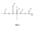
- Fig. 4 illustrates the output spectrum of the prior art quadrature modulator in the frequency domain when the base band input is a test tone.
- Fig. 5 is a system block diagram of a quadrature modulator according to the preferred embodiment which includes circuitry for calibrating the modulator.
- Fig. 6 illustrates the output spectrum of the preferred quadrature modulator in the frequency domain when a first test tone is applied thereto for the purposes of a calibration phase to eliminate carrier leakage
- Fig. 7 illustrates the output spectrum of the preferred quadrature modulator in the frequency domain when a second test tone, being one half the frequency of the first test tone, is applied to the modulator for the purposes of a second calibration phase to eliminate an undesired side band;
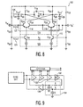
- Fig. 8 is a circuit diagram for an envelope detector employed in the preferred embodiment.
- Fig. 9 is a circuit diagram for a signal strength indicator and band pass filter employed on the preferred embodiment.
- Fig. 1 shows a quadrature transmitter 8 which includes an in-phase modulation branch 10 and a quadrature modulation branch 12.
- the in-phase branch 10 includes, in series arrangement, a base band dc offset adjustment block 16, a low pass filter 18, a base band gain adjustment amplifier 20, and mixer 22.
- the mixer 22 mixes an in-phase signal I(t) (an analog signal carrying digital information) with a sinusoidal carrier signal A c cos( ⁇ t )generated by a local oscillator (LO) 24.
- the quadrature phase branch 12 includes, in series arrangement, a dc base band offset adjustment block 17, a low pass filter 19, a gain adjustment amplifier 21, and a mixer 23.
- the mixer 23 mixes a quadrature signal Q(t) with a carrier signal A s sin( ⁇ t+ ⁇ e )that is generated by the local oscillator 24 and phase shifted 90°, in the ideal case, by a phase shift circuit such as a phase locked loop (PLL) 26.
- ⁇ e represents the phase shift error.
- the outputs of the mixers 22 and 23 are summed by a summer 28, the output of which is fed to a digitally programmable attenuator 30.
- the transmitter 8 operates on differential signals, and so the output of the attenuator 30 is fed to a transformer 32 which converts the differential signals to a single ended signal to be radiated through an antenna 34.
- a digital signal processor (DSP) 36 controls various circuits such as the DC offset adjustment blocks 16, 17, the gain amplifiers 20, 21, the PLL 26 and the attenuator 30.
- the DSP 36 also executes a calibration algorithm which is described in greater detail below.
- ⁇ LO is the local oscillator frequency
- I(t), Q(t) are the in-phase and quadrature signals, as discussed above.
- Equation [3] is referred to as the local oscillator (LO) feed-through or carrier leakage term because this component of the output spectrum is centered at ⁇ LO . It will be seen that if the dc offset adjustment can be properly adjusted at blocks 16 and 17, the LO feed-through can be eliminated or reduced.
- LO local oscillator
- Equation [4] is referred to as the "upper side band” (USB) term since this component of the output spectrum is centered at a frequency, ⁇ LO + ⁇ B which is higher than the local oscillator frequency.
- equation [5] is referred to as the "lower side band” (LSB) term since this component of the output spectrum is centered at ⁇ LO - ⁇ B , which is lower than the local oscillator frequency.
- the LSB will be the stronger frequency component and hence the desired signal, and the USB will be the weaker, and hence undesired signal.
- a base band gain mismatch, A I ⁇ A Q , a local oscillator level mismatch, A C ⁇ A S , and the local oscillator phase error ⁇ e are responsible for the residual USB term.
- the proper control of these system parameters can minimize the undesired sideband.
- efforts to minimize the undesired sideband to less than 50 dBc in the analog domain requires base band and high frequency gain matching on the order of 0.05dB and phase matching of 0.4 degrees. Conventional analog circuits do not allow such matching levels to be achieved.
- the present invention measures the output signal s(t) and adjusts the following system parameters A I , A Q ; V OI , V OQ ; and ⁇ e until the LO feed-through and USB components are minimized. This is accomplished by taking advantage of the fact that the LSB component will typically have a greater magnitude than the USB component or the LO feed-through.
- Fig. 3 exemplifies a two tone signal 40 in the time domain which is a sum of two sinusoidal components, A St cos( ⁇ st t ) + A we cos( ⁇ we t ), where the first component has a much higher amplitude than the second component. It will be seen from Fig.
- the envelope 42 (shown in stippled lines) of the two tone signal 40 is a sinusoid having the amplitude of the weak signal and a frequency equal to the difference between the two tones. More particularly, the envelope of the two tone signal 40 can be written as A St + A we cos( ⁇ st t - ⁇ we t ). Thus, if, for example, the weaker signal is the USB component and the stronger signal is the LSB component, measuring the envelope of such a two tone signal will enable the opportunity to adjust system parameters to reduce the level of the weaker or undesired signal.
- the output s ( t ) of the transmitter is not a two component signal but will have many frequency components.
- Fig. 4 illustrates a typical frequency spectrum for s ( t ) .
- the central axis is centered on the local oscillator frequency, e.g., at 1 GHz.
- Frequency component 44 represents the LO feed-through
- component 46 represents the USB
- component 48 represents the LSB.
- strong and weak 3 rd harmonics exist, as represented by components 50 and 52, respectively. Accordingly, as the output signal s ( t ) has multiple frequency components in addition to the desired component, the preferred embodiment filters at least some of the frequency components so that a two tone signal is substantially present.
- the higher harmonics being relatively small in amplitude, will not materially affect the shape of the envelope.
- the higher harmonics decrease substantially faster than the main signal the user will be able to reduce them by proper choice of the main signal levels (e.g. for every 1 dB reduction in the level of the LSB as in Fig. 4 , the 3 rd harmonics go down 3 dB).
- Fig. 5 is a system block diagram of a quadrature modulator 100 according to the preferred embodiment of the invention which employs a high dynamic range envelope detector 102, a band pass filter 104, and a signal strength indicator circuit 106.
- the detector 102 is positioned to detect s ( t ) at point A, at the output the attenuator 30.
- the detector 102 provides a signal at point B which represents the envelope of s ( t ) .
- This envelope is then filtered by the band pass filter 104 so as to allow through (at point C) the frequency component that should be minimized.
- the logarithmic signal strength indicator circuit 106 measures the strength of the passed-through frequency component and provides a signal 108 which is then used by the DSP 36 to adjust the system parameters of the modulator.
- the modulator is preferably calibrated in a two phase process. In the first phase, the LO feed-through is minimized and in the second phase the USB component is minimized, although in alternative embodiments these phases may be executed reversed in order.
- a first test tone e.g., 4 MHz
- the tones are generated by the DSP 36 or alternatively by any other known tone generator.
- the output spectrum at point A is as shown in Fig. 4 , having the desired LSB component 46, and smaller LO feed-through and USB components 44, 48 plus 2 nd and 3 rd harmonic components.
- the envelope detector 102 essentially shifts the frequency spectrum of the detected s ( t ) such that at point A, as shown in Fig.
- the LSB component 46 is shifted to zero frequency
- the LO feed-through component 44 is shifted to the frequency of the test tone, 4 MHz
- the USB component 48 is shifted to a frequency that is double that of the test tone.
- the band pass filter 104 is preferably configured with a sharp passband centered at 4 MHz which passes through substantially only the LO feed-through (as schematically illustrated in Fig. 6 ) 44, and thus controls the presence of various other undesired components.
- the logarithmic signal strength indicator 106 measures the level of the LO feed-through 44 and generates a signal which is used by the DSP 36 to minimize the LO feed-through 44.
- the LO feed-through 44 even though it may arise as a result of leakage through the substrate of the chip can be nulled out by adjusting the DC offset voltages V OI and V OQ so as to cause the LO feed-through 44 to cancel out at point A.
- V OI and V OQ are independent of each other and need to be separately nulled, thus requiring a two dimensional search to find the optimum values for the DC offsets.
- a second test tone at half the frequency of the first test tone e.g., 2 MHz, is applied to the I and Q base band inputs of the modulator.
- the frequency spectrum at point C resembles that shown in Fig. 7 , wherein the USB component 48 is separated from the LSB component 46 by twice the value of the second test tone signal.
- the signal strength indicator 106 generates the signal 108 which is used by the DSP 36 to adjust the base band gains A I or As at gain adjustment blocks 20, 21 and the local oscillator phase error ⁇ e at PLL 26 in order to minimize the USB component. This also requires a two dimensional search.
- the calibration process is of the "set and forget" type. It may be applied upon power up of the modulator, or at certain discrete instances such as inactive time slots. There is no need to continuously adjust the system parameters.
- the band pass filter 104 will reduce the effect of the strong 3 rd harmonic distortion component 50.
- the weak 3 rd harmonic component 52 falls directly on the sideband signal 48 after the envelope detector.
- the level of this distortion product is typically more than 60 dBc and is not likely to cause any problems. Its level can be reduced by 3dB for every dB of reduction in the main test tone signals I(t).and Q(t) during the calibration phase.
- a bandpass filter can be arranged prior to the envelope detector but that requires costly high Q filters that are impractical.
- the band pass filter can be a programmable band pass filter disposed after the detector to filter out undesired sidebands and harmonic products.
- the modulator 100 provides a large dynamic range capacity, for a number of reasons.
- the RF output level may need to be programmable, which is why the quadrature modulator 100 includes attenuators 30.
- the detector circuitry preferably detects the signal after the attenuation to minimize signal non-ideality at the point of delivery. Consequently, the level of the LSB component 46 could change dramatically.
- the level of the detected frequency component e.g. the LO-feed-through or USB component 48, e.g. from 15 dBc as a starting point to 50 dBc.
- the dynamic range of the detected signal can be quite high, e.g., 75 dB. For example, assuming a conventional -20 dBm.
- the signal strength indicator 106 should be sensitive to signals from -20 dBm to -95 dBm. In order to measure such a varying signal with consistent accuracy the signal strength indicator 106 is preferably implemented as a log amplifier/detector, as explained in greater detail below.
- a problem may exist since various undesired frequency components are present. These are all detected at the same time but controlled by different mechanisms. This is preferably solved by using a sharp band pass filter as described previously, followed by a limiter for the log detector.
- the band pass filter 104 pre-selects the frequency component for minimization and the limiter effectively eliminates the other undesired signals that can reduce the measurement accuracy.
- the limiter captures only the slightly stronger signals when two or more signals are present.
- Fig. 8 is a circuit diagram of the preferred embodiment of the envelope detector 102.
- the circuit which is based in part on a Gilbert cell provides considerably more dynamic range and superior signal to noise ratio than conventional envelope detectors, such as diode-based detectors.
- the circuit includes an upper tree 114 which includes two differential transistor pairs 116 and 118, comprising transistors Q 2A, Q 3A , Q 2B and Q 3B .
- the circuit 110 also includes a lower tree 120 which includes a second set of transistors Q 1 A and Q 1 B .
- the upper tree 114 is connected to the lower tree 120, as shown.
- a differential input signal is applied directly to the bases of the transistors of the upper tree 114 at input terminals V in + and V in - .
- the differential input signal is highly attenuated by a resistor divider network R 2 A , R 3 A , and R 2 B ,R 3 B and fed to the bases of the transistors of the lower tree 120.
- the lower tree 120 is highly degenerated in comparison to the upper tree 114.
- the upper tree transistors switch hard while the degenerated lower tree transistors see the input signal as well as its envelope. Referring back to figure 3 the upper tree only sees the zero crossings of the signal 40 and not aware of the envelope 42.
- the lower tree sees the whole signal 40.
- the upper and lower trees 114, 120 are used as a multiplier.
- the input signal applied to the upper tree 114 has a signal level exceeding the threshold voltage V T of the transistors (typically about 4V T , where V T ⁇ 25 mV pp ) whereas the amplitude of the input signal applied to the degenerate lower tree 120 is considerably lower than the threshold voltage (assuming that R 4 is zero ohms) due to R 2A , R 3A and R 2B , R 3B attenuators.
- the upper tree transistors are saturated and thus switch hard such that current flows through one side of the upper tree or the other, depending on the polarity of the input signal. This is schematically represented by square wave train 122.
- the transistors of the degenerated lower tree 120 do not switch hard, and the lower tree functions as an amplifier which is further linearized by the presence of R 4 , whereby the currents in the collects of Q 1 A and Q 1 B are reproductions of the voltages applied to the bases thereof.
- This is schematically represented by sinusoidal signal 124.
- the collectors of Q 2 A , Q 3 A and Q 2 B , Q 3 B all have a positive polarity, thus effectively multiplying the input signed by a synchronors square wave, as schematically represented by signal 126.
- a set of low pass filters comprising R 6 A C 2 A ; R 5' A , C 1 A + C 1 B ; R 5 B , C 1 A + C 1 B ; and R 6 B , C 2 B average the result so that at V out + and V out - the output is a differential low frequency signal 42 as shown in Figure 3 . Consequently, the output of the circuit 102 represents the envelope of the input signal. The net result is that the circuit shifts the spectral content of the input signal such that the frequency of the desired component, the LSB term in this example, is down converted to zero IF.
- R 1A , R 2A , R 3A and R 1B , R 2B , R 3B plus R 4 not part of a conventional Gilbert cell, provide simultaneous biasing for the upper tree and biasing plus attenuation for the lower tree for the optimal synchronous detector operation.
- Fig. 9 is a circuit diagram of the preferred embodiment of the signal strength indicator 106.
- the circuit employ a series of cascading amplifiers 130, 132 as known in the art per se to provide an output signal which is substantially equivalent to the log of the input signal. This enables a linear range of values, e.g. 1 to 5 volts, to represent variations in the level of the input signal on the order of 10 5 .
- a low pass filter 134 is incorporated in the feedback path in conjunction with an additional amplifier 136.
- the circuit effectively provides the band pass filter 104 of Fig. 5 with the low corner frequency being established by the values of R and C, and the high corner frequency being set by the bandwidth of the cascaded series of amplifiers. This results in a first order band pass filter. Higher order tunable active filters could also be placed between the synch detector of Fig. 9 and the secondary detector.
Landscapes
- Engineering & Computer Science (AREA)
- Computer Networks & Wireless Communication (AREA)
- Signal Processing (AREA)
- Digital Transmission Methods That Use Modulated Carrier Waves (AREA)
- Amplitude Modulation (AREA)
- Liquid Crystal (AREA)
- Analysing Materials By The Use Of Radiation (AREA)
Abstract
Description
- The invention relates to a quadrature modulator, a radio communication device comprising a quadrature modulator, and a method of calibrating the quadrature modulator or radio communication device.
- In a quadrature modulator, carrier leakage reduction and side band rejection have typically been carried out using one of two conventional methodologies. One of these methodologies depends on circuit matching, dynamic swapping, and the use of polyphase filters, all of which are carried out in the design phase. The second type of methodology deals with an imperfect chip but relies on user calibration methods while the chip is in use.
US-A-6,298,096 describes a transmit modulator which uses a quadrature modulator and which has a predistortion block which produces a predistorted output signal. The predistortion block pre-compensates for errors introduced by the quadrature modulator based on a set of predistortion parameters. The quadrature modulator receives the output signals from the predistortion block. The quadrature modulator up-converts the I and Q channel signals and combines them. In the process, the quadrature modulator introduces errors. In calibration mode, a sinusoidal wave at frequency f cal is applied to the input of the predistortion block and a transformer is coupled to the output of the quadrature modulator. The transformer produces a digital representation of a spectrum of the output of the quadrature modulator converted to baseband. Spurious energy produced by the quadrature modulator errors but reduced by the effect of the predistortion block is generated at f cal and 2*f cal. A quadratic polynomial minimization calculator receives the output of the transformer. The quadratic polynomial minimization calculator determines a subsequent value of the predistortion parameters based upon a quadratic relationship between energies present in the digital representation of the spectrum of the output of the quadrature modulator at frequencies f cal and 2*f cal and the values of the previous predistortion parameters.
InUS-A- 5,881,376 methods and systems for calibrating transceivers are described. Analog transceiver components create errors, such as gain and offset errors in a receiver or a transmitter portion, which are compensated by adjusting digital signal processing in the computing portion of the transceiver. Errors can be measured in a calibration procedure and determined compensating values stored in a memory device of the transceiver. These values can then be retrieved when the transceiver is initialized for usage during signal processing of signals received by and transmitted by the transceiver.
EP 0598 585 describes a Cartesian amplifier in which an input signal is preprocessed and split into two quadrature components. Both quadrature components are passed, in parallel, through an error amplifier (4), after which they are re-combined and up-converted to RF. The output of the amplifier is used to provide a feedback signal. This feedback is downconverted from RF to baseband and resolved into two quadrature components which are fed to the respective inputs of the error amplifier (4). Periodically the pre-processor (3) is switched into a calibration mode in which test signals are applied to the amplifier instead of the input signal. At these times the signal strength of the output of the power amplifier is measured and used to provide pre- distortion factors in the signal preprocessor (3) to improve amplifier linearity. - One example of the second methodology is disclosed in
U.S. 6,169,463 to Mohindra et al. which discloses a quadrature modulator with set and forget carrier leakage compensation. Upon the power-up of the quadrature modulator, carrier leakage is measured in the in-phase and quadrature branches through the use of a synchronous detector. A state machine starts signal generators which inject compensation signals into the in-phase and quadrature branches, respectively, so that DC offsets in these branches are reduced thereby reducing the carrier leakage. Mohindra does not, however, disclose the rejection of undesired side bands. Mohindra proposes a simple detection scheme which can be difficult to implement since it does not distinguish between carrier leakage and side-tones or other errors. Also the large dynamic range of the signals that have to be suppressed require cumbersome and slow "gain-set" and "error-detect" sequences that have to be implemented in software. - It is desirable to not only suppress the carrier leakage but also to reduce undesired sidebands using minimal, and low cost, circuitry. It is also desirable to minimize the search for appropriate circuit parameters to reduce these undesirable circuit parameters.
- One aspect of the invention relates to a method of calibrating a quadrature modulator. The method includes: applying a first test tone signal to an in-phase modulation branch input of the modulator and a ninety degree phase-shifted version of the first test tone signal to a quadrature modulation branch input of the modulator; measuring the level of a local oscillator (LO) feedthrough in an output signal of the modulator and in response adjusting base band dc offset voltages to minimize the LO feedthrough; applying a second test tone signal to the in-phase modulation branch input and a ninety degree phase-shifted version of the second test tone signal to the quadrature modulation branch input; and measuring the level of an undesired upper sideband frequency component in the output signal and in response adjusting base band gains the in-phase and quadrature modulation branches and a LO phase error to minimize the undesired side band.
- In the preferred embodiment, the level of the local oscillator (LO) feedthrough or the undesired sideband in the output signal is measured by: shifting the frequency spectrum of the output signal such that a lower sideband frequency component (LSB) is down-converted to zero IF; filtering the spectrum-shifted signal to pass through either the LO feedthrough or the undesired sideband, such as an upper sideband; and measuring the amplitude of the filtered, spectrum-shifted signal.
- Another aspect of the invention relates to a quadrature modulator which includes an in-phase modulation branch and a quadrature modulation branch. The in-phase modulation branch receives an analog in-phase base band signal as an input, and includes a first dc offset adjustment circuit, a first base band gain adjustment circuit, and a first mixer. The quadrature modulation branch receives an analog quadrature based band signal as an input, and includes a second dc offset adjustment circuit, a second base band gain adjustment circuit, and a second mixer. A local oscillator means provides a local oscillator signal to the first mixer and a phase shifted version of the local oscillator signal to the second mixer. A summer sums the outputs of the first and second mixers. An envelope detector detects an output signal of the modulator and provides a signal representative of the amplitude of the output signal. A band pass filter filters the amplitude signal. A signal strength indicator circuit measures the strength of the filtered amplitude signal, and provides a compensation signal for adjusting the phase shift of the local oscillator and the dc offsets and base band gains of the in-phase and quadrature base band signals.
- In the preferred embodiment the envelope detector is a synchronous detector and the signal strength indicator is a log indicator. Means are provided for applying a first test tone signal to the in-phase modulation branch input and a ninety degree phase-shifted version of the first test tone signal to the quadrature modulation branch input. The compensation signal is employed to minimize carrier leakage in the output signal by adjusting the base band dc offsets in the in-phase and quadrature branches. A second test tone signal is then applied to the in-phase modulation branch input and a ninety degree phase-shifted version of the second test tone signal is applied to the quadrature modulation branch input. The second test tone has a frequency that is substantially one half of the frequency of the first test tone. The compensation signal to is employed minimize an undesired upper sideband frequency component in the output signal by adjusting the base band gains the in-phase and quadrature modulation branches and the phase shift of the local oscillator signal.
- The preferred synchronous envelope detector comprises a Gilbert cell having at least one differential transistor pair in an upper branch and at least one transistor in a lower branch, the upper and lower branches being interconnected, with each of the upper and lower branches having input terminals. A resistor divider network is connected between the input terminals of the upper branch and the input terminals of the lower branch. The resistive values of the network are selected such that a selected input signal having a signal level sufficient to saturate the transistors of the upper branch is attenuated so as to not saturate the transistors of the lower branch. A low pass filter is connected to the upper branch of transistors, and an output signal of the detector is provided at the low pass filter.
-
Fig. 1 is a system block diagram of a prior art quadrature modulator. -
Fig. 2 illustrates the existence of various non-idealities in the quadrature modulator ofFig. 1 . -
Fig. 3 illustrates the waveform of a two-tone signal in the time domain. -
Fig. 4 illustrates the output spectrum of the prior art quadrature modulator in the frequency domain when the base band input is a test tone. -
Fig. 5 is a system block diagram of a quadrature modulator according to the preferred embodiment which includes circuitry for calibrating the modulator. -
Fig. 6 illustrates the output spectrum of the preferred quadrature modulator in the frequency domain when a first test tone is applied thereto for the purposes of a calibration phase to eliminate carrier leakage; -
Fig. 7 illustrates the output spectrum of the preferred quadrature modulator in the frequency domain when a second test tone, being one half the frequency of the first test tone, is applied to the modulator for the purposes of a second calibration phase to eliminate an undesired side band; -
Fig. 8 is a circuit diagram for an envelope detector employed in the preferred embodiment. -
Fig. 9 is a circuit diagram for a signal strength indicator and band pass filter employed on the preferred embodiment. -
Fig. 1 shows aquadrature transmitter 8 which includes an in-phase modulation branch 10 and aquadrature modulation branch 12. The in-phase branch 10 includes, in series arrangement, a base band dcoffset adjustment block 16, alow pass filter 18, a base bandgain adjustment amplifier 20, andmixer 22. Themixer 22 mixes an in-phase signal I(t) (an analog signal carrying digital information) with a sinusoidal carrier signal Ac cos(ωt)generated by a local oscillator (LO) 24. Thequadrature phase branch 12 includes, in series arrangement, a dc base band offsetadjustment block 17, alow pass filter 19, again adjustment amplifier 21, and amixer 23. Themixer 23 mixes a quadrature signal Q(t) with a carrier signal As sin(ωt+φe)that is generated by thelocal oscillator 24 and phase shifted 90°, in the ideal case, by a phase shift circuit such as a phase locked loop (PLL) 26. φe represents the phase shift error. - The outputs of the
mixers summer 28, the output of which is fed to a digitallyprogrammable attenuator 30. In the preferred embodiment thetransmitter 8 operates on differential signals, and so the output of theattenuator 30 is fed to atransformer 32 which converts the differential signals to a single ended signal to be radiated through anantenna 34. - A digital signal processor (DSP) 36 controls various circuits such as the DC offset adjustment blocks 16, 17, the
gain amplifiers PLL 26 and theattenuator 30. TheDSP 36 also executes a calibration algorithm which is described in greater detail below. - A number of imperfections or non-idealities are present in the
quadrature transmitter 8 as shown, and in other quadrature transmitters similar thereto. These non-idealities arise, inter alia, from the following sources, as indicated inFig. 2 : - AI, AQ
- Baseband gain in the in-phase and quadrature branches, respectively, which may not be equal
- VOI, VOQ
- Built-in equivalent dc offset voltage in the in-phase and quadrature branches, respectively, which may not be zero
- AC, AS
- Local oscillator amplitudes in the in-phase and quadrature branches, respectively, which may not be equal
- VOC, VOS
- Local oscillator equivalent offset voltages in the in-phase and quadrature branches, respectively, which may not be zero
- φe
- Local oscillator quadrature phase error
- Consequently, the transmit signal, s(t), can be written in the following general form:

where
ωLO is the local oscillator frequency, and
I(t), Q(t) are the in-phase and quadrature signals, as discussed above.
It will be seen from equation [1] that if the non-idealities are eliminated, s(t)reduces to an ideal quadrature signal:
- If the input baseband signals are defined as I(t) = VI cos(ωBt) and Q(t) = VQ sin(ωBt), expanding equation [1] yields three major terms as follows:


- Equation [3] is referred to as the local oscillator (LO) feed-through or carrier leakage term because this component of the output spectrum is centered at ωLO. It will be seen that if the dc offset adjustment can be properly adjusted at
blocks - Equation [4] is referred to as the "upper side band" (USB) term since this component of the output spectrum is centered at a frequency, ωLO + ωB which is higher than the local oscillator frequency. Similarly, equation [5] is referred to as the "lower side band" (LSB) term since this component of the output spectrum is centered at ωLO - ωB, which is lower than the local oscillator frequency.
- Assuming positive parameters, the LSB will be the stronger frequency component and hence the desired signal, and the USB will be the weaker, and hence undesired signal. From equation [4], it will be seen that a base band gain mismatch, AI ≠ AQ, a local oscillator level mismatch, AC ≠ AS, and the local oscillator phase error φe are responsible for the residual USB term. The proper control of these system parameters can minimize the undesired sideband. However, efforts to minimize the undesired sideband to less than 50 dBc in the analog domain requires base band and high frequency gain matching on the order of 0.05dB and phase matching of 0.4 degrees. Conventional analog circuits do not allow such matching levels to be achieved.
- Rather than trying to improve matching and phase control by either improved layouts or dynamic techniques, the present invention measures the output signal s(t) and adjusts the following system parameters AI, AQ ; VOI , VOQ; and φe until the LO feed-through and USB components are minimized. This is accomplished by taking advantage of the fact that the LSB component will typically have a greater magnitude than the USB component or the LO feed-through.
Fig. 3 exemplifies a twotone signal 40 in the time domain which is a sum of two sinusoidal components, ASt cos(ω stt) + Awe cos(ω wet), where the first component has a much higher amplitude than the second component. It will be seen fromFig. 3 that the envelope 42 (shown in stippled lines) of the twotone signal 40 is a sinusoid having the amplitude of the weak signal and a frequency equal to the difference between the two tones. More particularly, the envelope of the twotone signal 40 can be written as ASt + Awe cos(ω stt - ω wet). Thus, if, for example, the weaker signal is the USB component and the stronger signal is the LSB component, measuring the envelope of such a two tone signal will enable the opportunity to adjust system parameters to reduce the level of the weaker or undesired signal. - In practice, however, the output s(t) of the transmitter, is not a two component signal but will have many frequency components.
Fig. 4 illustrates a typical frequency spectrum for s(t). In this plot, the central axis is centered on the local oscillator frequency, e.g., at 1 GHz.Frequency component 44 represents the LO feed-through,component 46 represents the USB andcomponent 48 represents the LSB. In addition, strong and weak 3rd harmonics exist, as represented bycomponents Fig. 4 , the 3rd harmonics go down 3 dB). -
Fig. 5 is a system block diagram of aquadrature modulator 100 according to the preferred embodiment of the invention which employs a high dynamicrange envelope detector 102, aband pass filter 104, and a signal strength indicator circuit 106. Thedetector 102 is positioned to detect s(t) at point A, at the output theattenuator 30. Thedetector 102 provides a signal at point B which represents the envelope of s(t). This envelope is then filtered by theband pass filter 104 so as to allow through (at point C) the frequency component that should be minimized. The logarithmic signal strength indicator circuit 106 measures the strength of the passed-through frequency component and provides asignal 108 which is then used by theDSP 36 to adjust the system parameters of the modulator. - The modulator is preferably calibrated in a two phase process. In the first phase, the LO feed-through is minimized and in the second phase the USB component is minimized, although in alternative embodiments these phases may be executed reversed in order.
- In the preferred first phase, a first test tone, e.g., 4 MHz, is applied to the I and Q base band inputs of the transmitter (the tone applied at the Q input being 90 degrees out of phase with the tone applied at the I input). The tones are generated by the
DSP 36 or alternatively by any other known tone generator. The output spectrum at point A is as shown inFig. 4 , having the desiredLSB component 46, and smaller LO feed-through andUSB components envelope detector 102 essentially shifts the frequency spectrum of the detected s(t) such that at point A, as shown inFig. 6 , theLSB component 46 is shifted to zero frequency, the LO feed-throughcomponent 44 is shifted to the frequency of the test tone, 4 MHz, and theUSB component 48 is shifted to a frequency that is double that of the test tone. Theband pass filter 104 is preferably configured with a sharp passband centered at 4 MHz which passes through substantially only the LO feed-through (as schematically illustrated inFig. 6 ) 44, and thus controls the presence of various other undesired components. The logarithmic signal strength indicator 106 measures the level of the LO feed-through 44 and generates a signal which is used by theDSP 36 to minimize the LO feed-through 44. The LO feed-through 44, even though it may arise as a result of leakage through the substrate of the chip can be nulled out by adjusting the DC offset voltages VOI and VOQ so as to cause the LO feed-through 44 to cancel out at point A. Note that VOI and VOQ are independent of each other and need to be separately nulled, thus requiring a two dimensional search to find the optimum values for the DC offsets.
In the second phase of the calibration process, once the LO feed-through 44 has been minimized, a second test tone at half the frequency of the first test tone, e.g., 2 MHz, is applied to the I and Q base band inputs of the modulator. After passing through theenvelope detector 102 the frequency spectrum at point C resembles that shown inFig. 7 , wherein theUSB component 48 is separated from theLSB component 46 by twice the value of the second test tone signal. This allows the very same band pass filter 106 to be used to propagate substantially only the USB component 48 (as schematically illustrated inFig. 7 ) to the logarithmic signal strength indicator 106. The signal strength indicator 106 generates thesignal 108 which is used by theDSP 36 to adjust the base band gains AI or As at gain adjustment blocks 20, 21 and the local oscillator phase error φe atPLL 26 in order to minimize the USB component. This also requires a two dimensional search. - The calibration process is of the "set and forget" type. It may be applied upon power up of the modulator, or at certain discrete instances such as inactive time slots. There is no need to continuously adjust the system parameters.
- Note that the
band pass filter 104 will reduce the effect of the strong 3rdharmonic distortion component 50. The weak 3rdharmonic component 52, however, falls directly on thesideband signal 48 after the envelope detector. The level of this distortion product is typically more than 60 dBc and is not likely to cause any problems. Its level can be reduced by 3dB for every dB of reduction in the main test tone signals I(t).and Q(t) during the calibration phase. - A bandpass filter can be arranged prior to the envelope detector but that requires costly high Q filters that are impractical. Those skilled in the art will the band pass filter can be a programmable band pass filter disposed after the detector to filter out undesired sidebands and harmonic products.
- In the preferred embodiment the
modulator 100 provides a large dynamic range capacity, for a number of reasons. First, the RF output level may need to be programmable, which is why thequadrature modulator 100 includesattenuators 30. The detector circuitry preferably detects the signal after the attenuation to minimize signal non-ideality at the point of delivery. Consequently, the level of theLSB component 46 could change dramatically. - Second, it is desired to reduce considerably the level of the detected frequency component, e.g. the LO-feed-through or
USB component 48, e.g. from 15 dBc as a starting point to 50 dBc. Adding the variation of the main signal due to the RF level adjustments in the output attenuator, e.g. 25 dB, the dynamic range of the detected signal can be quite high, e.g., 75 dB. For example, assuming a conventional -20 dBm. If level at 1.5 GHz with a 25 dB on-chip programmable attenuator and a requirement that the side bands be suppressed by 50 dB, the signal strength indicator 106 should be sensitive to signals from -20 dBm to -95 dBm. In order to measure such a varying signal with consistent accuracy the signal strength indicator 106 is preferably implemented as a log amplifier/detector, as explained in greater detail below. - Third, a problem may exist since various undesired frequency components are present. These are all detected at the same time but controlled by different mechanisms. This is preferably solved by using a sharp band pass filter as described previously, followed by a limiter for the log detector. The
band pass filter 104 pre-selects the frequency component for minimization and the limiter effectively eliminates the other undesired signals that can reduce the measurement accuracy. The limiter captures only the slightly stronger signals when two or more signals are present. -
Fig. 8 is a circuit diagram of the preferred embodiment of theenvelope detector 102. The circuit, which is based in part on a Gilbert cell provides considerably more dynamic range and superior signal to noise ratio than conventional envelope detectors, such as diode-based detectors. The circuit includes anupper tree 114 which includes two differential transistor pairs 116 and 118, comprising transistors Q2A, Q3A, Q2B and Q3B. The circuit 110 also includes alower tree 120 which includes a second set of transistors Q 1A and Q 1 B. Theupper tree 114 is connected to thelower tree 120, as shown. - A differential input signal is applied directly to the bases of the transistors of the
upper tree 114 at input terminals

lower tree 120. Thelower tree 120 is highly degenerated in comparison to theupper tree 114. The upper tree transistors switch hard while the degenerated lower tree transistors see the input signal as well as its envelope. Referring back tofigure 3 the upper tree only sees the zero crossings of thesignal 40 and not aware of theenvelope 42. The lower tree sees thewhole signal 40. - Therefore, the upper and
lower trees upper tree 114 has a signal level exceeding the threshold voltage VT of the transistors (typically about 4VT, where VT ≈ 25 mVpp) whereas the amplitude of the input signal applied to the degeneratelower tree 120 is considerably lower than the threshold voltage (assuming that R 4 is zero ohms) due to R2A , R3A and R2B , R3B attenuators. The upper tree transistors are saturated and thus switch hard such that current flows through one side of the upper tree or the other, depending on the polarity of the input signal. This is schematically represented bysquare wave train 122. In contrast, the transistors of the degeneratedlower tree 120 do not switch hard, and the lower tree functions as an amplifier which is further linearized by the presence of R4, whereby the currents in the collects of Q 1 A and Q 1 B are reproductions of the voltages applied to the bases thereof. [This is schematically represented bysinusoidal signal 124. However, as a result of the hard switching of the upper tree transistors the currents in the collectors of Q 1 A and Q 1 B are chopped off. At the output, the collectors of Q 2 A, Q 3 A and Q 2B , Q 3 B all have a positive polarity, thus effectively multiplying the input signed by a synchronors square wave, as schematically represented bysignal 126. - A set of low pass filters, comprising R 6 AC 2A ;R 5'A ,C 1 A + C 1B ;R 5B ,C 1 A + C 1B ; and R 6B ,C 2 B average the result so that at


low frequency signal 42 as shown inFigure 3 . Consequently, the output of thecircuit 102 represents the envelope of the input signal. The net result is that the circuit shifts the spectral content of the input signal such that the frequency of the desired component, the LSB term in this example, is down converted to zero IF. The combination of R1A, R2A, R3A and R1B , R2B, R3B plus R4, not part of a conventional Gilbert cell, provide simultaneous biasing for the upper tree and biasing plus attenuation for the lower tree for the optimal synchronous detector operation. -
Fig. 9 is a circuit diagram of the preferred embodiment of the signal strength indicator 106. The circuit employ a series of cascadingamplifiers 130, 132 as known in the art per se to provide an output signal which is substantially equivalent to the log of the input signal. This enables a linear range of values, e.g. 1 to 5 volts, to represent variations in the level of the input signal on the order of 105. Alow pass filter 134 is incorporated in the feedback path in conjunction with anadditional amplifier 136. The circuit effectively provides theband pass filter 104 ofFig. 5 with the low corner frequency being established by the values of R and C, and the high corner frequency being set by the bandwidth of the cascaded series of amplifiers. This results in a first order band pass filter. Higher order tunable active filters could also be placed between the synch detector ofFig. 9 and the secondary detector. - The preferred embodiment has been shown and described as operating with differential signals. Those skilled in the art will understand that the preferred embodiment may be readily varied to operate with single ended signals.
Claims (13)
- A method of calibrating a quadrature modulator, comprising:a) applying a first test tone signal to an in-phase modulation branch input of the modulator and a ninety degree phase-shifted version of the first test tone signal to a quadrature modulation branch input of the modulator;b) measuring the level of a local oscillator (LO) feedthrough in an output signal of the modulator and in response adjusting base band dc offset voltages to minimize the LO feedthrough;c) applying a second test tone signal to the in-phase modulation branch input and a ninety degree phase-shifted version of the second test tone signal to the quadrature modulation branch input; characterized in that it further comprisesd) measuring the level of an undesired upper sideband frequency component in the output signal and in response adjusting base band gains of the in-phase and quadrature modulation branches and a LO phase error to minimize the undesired sideband.
- A method according to claim 1, wherein the second test tone has a frequency that is substantially one half of the frequency of the first test tone.
- A method according to claim 1, wherein measuring the level of the local oscillator (LO) feedthrough or the USB in the output signal is carried out by:a) shifting the frequency spectrum of the output signal such that a lower sideband frequency component (LSB) is down-converted to zero IF;b) filtering the spectrum-shifted signal to pass through either the LO feedthrough or the USB; andc) measuring the amplitude of the filtered, spectrum-shifted signal.
- A method according to claim 3, wherein the frequency spectrum of the output signal is shifted by a synchronous envelope detector.
- A method according to claim 3, wherein the amplitude of the filtered, spectrum-shifted signal is measured by a log detector which provides a compensation signal employed to minimize the LO feedthrough or undesired sideband.
- A method according to claim 5, including selectively attenuating the output signal prior to the step of measuring the output signal.
- A method according to claim 4, wherein the second test tone has a frequency that is substantially one half of the frequency of the first test tone.
- A quadrature modulator, comprising:a) an in-phase modulation branch for receiving an analog in-phase base band signal,b) a quadrature modulation branch for receiving an analog quadrature base band signal,c) a local oscillator means for providing a local oscillator signal to a first mixer included in said in-phase modulation branch and a phase shifted version of the local oscillator signal to a second mixer included in said quadrature modulation branch;d) a summer for summing output signals provided by the in-phase modulation branch and the quadrature modulation branch,e) an envelope detector for detecting an output signal of the modulator and providing a signal representative of the amplitude of the output signal;f) a band pass filter for filtering the amplitude signal; characterized in that it further comprises:g) a signal strength indicator circuit for measuring a level of a local oscillator feedthrough in an output signal of the modulator during a first phase, and a level of an undesired upper sideband frequency component in the output signal during a second phase, the indicator circuit providing a compensation signal for adjusting the phase shift of a local oscillator and the dc offsets and base band gains of the in-phase and quadrature base band signalsh) means for:i) applying a first test tone signal to the in-phase modulation branch input and a ninety degree phase-shifted version of the first test tone signal to the quadrature modulation branch input;j) employing the compensation signal to minimize the local oscillator feedthrough;k) applying a second test tone signal to the in-phase modulation branch input and a ninety degree phase-shifted version of the second test tone signal to the quadrature modulation branch input, andl) employing the compensation signal to minimize an undesired upper sideband frequency component in the output signal by adjusting the base band gains of the in-phase and quadrature modulation branches and the phase shift of the local oscillator signal.
- A modulator according to claim 8, wherein the envelope detector is a synchronous detector and the signal strength indicator is a log indicator.
- A modulator according to claim 9, including a programmable attenuator for adjusting the level of the output signal, and wherein the envelope detector measures the output signal following attenuation.
- A modulator according to claim 8, wherein the envelope detector, comprises:a) a Gilbert cell having at least one differential transistor pair in an upper branch and at least one transistor in a lower branch, the upper and lower branches being interconnected, each of the upper and lower branches having input terminals;b) a resistor divider network connected between the input terminals of the upper branch and the input terminals of the lower branch, the resistive values of the network being selected such that a selected input signal having a signal level sufficient to saturate the transistors of the upper branch is attenuated so as to not saturate the transistors of the lower branch; andc) low pass filter means connected to the upper branch of transistors, an output signal of the detector being provided at the low pass filter.
- A modulator according to claim 11, wherein the lower branch of the envelope detector has two BJT transistors and a resistor is connected between the emitters of the transistors.
- A modulator according to claim 11, wherein the envelope detector further includes means for biasing the transistors of the upper branch.
Applications Claiming Priority (2)
| Application Number | Priority Date | Filing Date | Title |
|---|---|---|---|
| US46512703P | 2003-04-24 | 2003-04-24 | |
| PCT/IB2004/001191 WO2004095686A2 (en) | 2003-04-24 | 2004-04-20 | Quadrature modulator and calibration method |
Publications (2)
| Publication Number | Publication Date |
|---|---|
| EP1620940A2 EP1620940A2 (en) | 2006-02-01 |
| EP1620940B1 true EP1620940B1 (en) | 2010-02-17 |
Family
ID=33310994
Family Applications (1)
| Application Number | Title | Priority Date | Filing Date |
|---|---|---|---|
| EP04728374A Expired - Lifetime EP1620940B1 (en) | 2003-04-24 | 2004-04-20 | Quadrature modulator and calibration method |
Country Status (8)
| Country | Link |
|---|---|
| US (2) | US7548591B2 (en) |
| EP (1) | EP1620940B1 (en) |
| JP (1) | JP4555898B2 (en) |
| KR (1) | KR101023382B1 (en) |
| CN (2) | CN100472941C (en) |
| AT (1) | ATE458301T1 (en) |
| DE (1) | DE602004025561D1 (en) |
| WO (1) | WO2004095686A2 (en) |
Families Citing this family (45)
| Publication number | Priority date | Publication date | Assignee | Title |
|---|---|---|---|---|
| CN100472941C (en) | 2003-04-24 | 2009-03-25 | 皇家飞利浦电子股份有限公司 | Quadrature modulator and its calibration method |
| EP1633096A1 (en) * | 2004-08-26 | 2006-03-08 | St Microelectronics S.A. | Carrier and symbol frequency determination of a signal |
| US7734261B2 (en) | 2004-12-16 | 2010-06-08 | Nxp B.V. | Calibrating amplitude and phase imbalance and DC offset of an analog I/Q modulator in a high-frequency transmitter |
| JP4063824B2 (en) * | 2005-01-12 | 2008-03-19 | 埼玉日本電気株式会社 | Wireless communication device |
| US8032095B1 (en) * | 2005-03-03 | 2011-10-04 | Marvell International Ltd. | Method and apparatus for detecting carrier leakage in a wireless or similar system |
| US7750751B2 (en) * | 2005-03-08 | 2010-07-06 | Keith Jay Bertrand | Method and apparatus for creating phase modulation in edge-sensitive signals |
| JP2007104007A (en) * | 2005-09-30 | 2007-04-19 | Toshiba Corp | Quadrature modulator and vector correction method in quadrature modulator |
| US20070109955A1 (en) * | 2005-11-11 | 2007-05-17 | Broadcom Corporation, A California Corporation | Power control in MIMO transceiver |
| DE102006027557B4 (en) * | 2006-06-14 | 2010-07-15 | Atmel Automotive Gmbh | System for calibrating at least one quadrature modulator and operating method therefor |
| US7760817B2 (en) * | 2006-08-10 | 2010-07-20 | Mediatek Inc. | Communication system for utilizing single tone testing signal having specific frequency or combinations of DC value and single tone testing signal to calibrate impairments in transmitting signal |
| KR101261527B1 (en) * | 2006-10-27 | 2013-05-06 | 삼성전자주식회사 | Method and apparatus for compensating for mismatch occurred in radio frequency quadrature transceiver using direct-conversion scheme |
| KR101334923B1 (en) | 2007-03-09 | 2013-11-29 | 삼성전자주식회사 | Apparatus and method quadrature modulation in communication system |
| US7941106B2 (en) * | 2007-05-10 | 2011-05-10 | Skyworks Solutions, Inc. | Systems and methods for controlling local oscillator feed-through |
| US8045660B1 (en) | 2007-05-23 | 2011-10-25 | Hypres, Inc. | Wideband digital spectrometer |
| KR100961260B1 (en) * | 2007-12-04 | 2010-06-03 | 한국전자통신연구원 | Carrier Leak Compensation Device and Method in Orthogonal Modulation System |
| US7925228B2 (en) * | 2008-02-29 | 2011-04-12 | Stmicroelectronics, S.R.L. | Method and system for calibrating quadrature modulators |
| US7953379B2 (en) * | 2008-02-29 | 2011-05-31 | Stmicroelectronics, S.R.L. | Method and system for calibrating quadrature modulators |
| TWI357746B (en) * | 2008-04-25 | 2012-02-01 | Univ Nat Taiwan | Signal modulation device and signal amplifier |
| US8175549B2 (en) * | 2008-10-17 | 2012-05-08 | Texas Instruments Incorporated | Closed loop transmitter IQ calibration |
| CN101447958B (en) * | 2008-12-30 | 2011-05-11 | 清华大学 | Measurement method for performance of modulator and device thereof |
| US9496620B2 (en) * | 2013-02-04 | 2016-11-15 | Ubiquiti Networks, Inc. | Radio system for long-range high-speed wireless communication |
| JP5287521B2 (en) * | 2009-06-04 | 2013-09-11 | 株式会社リコー | Communication device |
| JP2011188436A (en) * | 2010-03-11 | 2011-09-22 | Advantest Corp | Measuring device, measuring method, and program therefor |
| US8415999B2 (en) | 2010-07-28 | 2013-04-09 | International Business Machines Corporation | High frequency quadrature PLL circuit and method |
| US20120294343A1 (en) * | 2011-05-16 | 2012-11-22 | Phase Matrix, Inc. | RF I/Q Modulator with Sampling Calibration System |
| US8774316B2 (en) | 2011-07-13 | 2014-07-08 | Harris Corporation | Transmitter including calibration of an in-phase/quadrature (I/Q) modulator and associated methods |
| US8787498B2 (en) | 2011-08-18 | 2014-07-22 | L-3 Communications Cincinnati Electronics Corporation | Systems and methods for enhanced carrier suppression |
| JP5960465B2 (en) * | 2012-03-28 | 2016-08-02 | パナソニック株式会社 | Transmitter, signal generation apparatus, and signal generation method |
| US20160218406A1 (en) | 2013-02-04 | 2016-07-28 | John R. Sanford | Coaxial rf dual-polarized waveguide filter and method |
| US9136989B2 (en) | 2013-10-10 | 2015-09-15 | Motorola Solutions, Inc. | Method and apparatus for reducing carrier leakage |
| EP3055930B1 (en) | 2013-10-11 | 2019-11-20 | Ubiquiti Inc. | Wireless radio system optimization by persistent spectrum analysis |
| CN104981941B (en) | 2014-04-01 | 2018-02-02 | 优倍快网络公司 | antenna assembly |
| WO2016003864A1 (en) | 2014-06-30 | 2016-01-07 | Ubiquiti Networks, Inc. | Wireless radio device alignment tools and methods |
| JP6267250B2 (en) * | 2016-02-25 | 2018-01-24 | 株式会社Subaru | Hydraulic circuit abnormality detection device and hydraulic circuit abnormality detection method |
| US10395542B2 (en) * | 2016-03-28 | 2019-08-27 | Cisco Technology, Inc. | Drone traffic engineering |
| JP7059639B2 (en) * | 2018-01-11 | 2022-04-26 | 富士通株式会社 | Clog determination device |
| US10727790B2 (en) * | 2018-04-26 | 2020-07-28 | Qualcomm Incorporated | Driver amplifier with programmable single-ended and differential outputs |
| CN109379146B (en) * | 2018-12-27 | 2021-01-29 | 中国电子科技集团公司第七研究所 | A Circuit Parameter Correction Method of Quadrature Modulator |
| US11405042B2 (en) * | 2019-12-31 | 2022-08-02 | Texas Instruments Incorporated | Transceiver carrier frequency tuning |
| US11646919B2 (en) * | 2020-01-08 | 2023-05-09 | Mediatek Singapore Pte. Ltd. | IQ generator for mixer |
| CN113253241B (en) * | 2021-06-01 | 2022-08-02 | 哈尔滨工业大学 | Method for processing sweep frequency interference ranging signal |
| JP7754701B2 (en) * | 2021-12-13 | 2025-10-15 | Necスペーステクノロジー株式会社 | Modulator, modulation method, signal transmitter and signal transmission method |
| CN114050874B (en) * | 2022-01-12 | 2022-04-12 | 中星联华科技(北京)有限公司 | Modulation calibration circuit and method |
| CN114726317B (en) * | 2022-04-26 | 2025-05-16 | 中国电子科技集团公司第五十八研究所 | A high linearity broadband quadrature modulator |
| CN114866035B (en) * | 2022-06-06 | 2025-01-24 | 中国电子科技集团公司第五十八研究所 | A broadband and high modulation accuracy RF quadrature modulator |
Family Cites Families (15)
| Publication number | Priority date | Publication date | Assignee | Title |
|---|---|---|---|---|
| GB2213006B (en) | 1987-11-27 | 1992-01-29 | Stc Plc | Correction of rf errors in quadrature channels of a zero-if transmitter |
| GB2272589B (en) * | 1992-11-16 | 1995-11-29 | Linear Modulation Tech | Automatic calibration of the quadrature balance within a cartesian amplifier |
| US5396196A (en) | 1993-12-29 | 1995-03-07 | At&T Corp. | Quadrature modular with adaptive suppression of carrier leakage |
| US5893030A (en) * | 1994-05-25 | 1999-04-06 | Oki Telecom | Dual-function double balanced mixer circuit |
| US5881376A (en) * | 1995-12-15 | 1999-03-09 | Telefonaktiebolaget Lm Ericsson | Digital calibration of a transceiver |
| JP3125717B2 (en) * | 1997-05-30 | 2001-01-22 | 日本電気株式会社 | Wireless communication device using quadrature modulation / demodulation circuit |
| US5907261A (en) * | 1997-09-05 | 1999-05-25 | Ericsson Inc. | Method and apparatus for controlling signal amplitude level |
| US6167247A (en) * | 1998-07-15 | 2000-12-26 | Lucent Technologies, Inc. | Local oscillator leak cancellation circuit |
| US6298096B1 (en) * | 1998-11-19 | 2001-10-02 | Titan Corporation | Method and apparatus for determination of predistortion parameters for a quadrature modulator |
| US6169463B1 (en) | 1999-03-24 | 2001-01-02 | Philips Electronic North America Corp. | Quadrature modulator with set-and-forget carrier leakage compensation |
| US6421397B1 (en) | 2000-01-28 | 2002-07-16 | Alcatel Canada Inc. | Modulation system having on-line IQ calibration |
| US6745015B2 (en) * | 2001-02-08 | 2004-06-01 | Motorola, Inc. | Method for automatic carrier suppression tuning of a wireless communication device |
| US6771709B2 (en) * | 2001-10-16 | 2004-08-03 | Her Majesty The Queen In Right Of Canada, As Represented By The Minister Of Industry | System and method for direct transmitter self-calibration |
| CN100472941C (en) | 2003-04-24 | 2009-03-25 | 皇家飞利浦电子股份有限公司 | Quadrature modulator and its calibration method |
| US7769361B2 (en) * | 2006-07-19 | 2010-08-03 | Qualcomm Incorporated | Systems, methods, and apparatus for frequency conversion |
-
2004
- 2004-04-20 CN CNB2004800109545A patent/CN100472941C/en not_active Expired - Lifetime
- 2004-04-20 EP EP04728374A patent/EP1620940B1/en not_active Expired - Lifetime
- 2004-04-20 KR KR1020057019982A patent/KR101023382B1/en not_active Expired - Lifetime
- 2004-04-20 AT AT04728374T patent/ATE458301T1/en not_active IP Right Cessation
- 2004-04-20 US US10/554,020 patent/US7548591B2/en not_active Expired - Lifetime
- 2004-04-20 CN CN2008101308851A patent/CN101355343B/en not_active Expired - Lifetime
- 2004-04-20 JP JP2006506490A patent/JP4555898B2/en not_active Expired - Lifetime
- 2004-04-20 WO PCT/IB2004/001191 patent/WO2004095686A2/en not_active Ceased
- 2004-04-20 DE DE602004025561T patent/DE602004025561D1/en not_active Expired - Fee Related
-
2009
- 2009-06-15 US US12/484,544 patent/US7893758B2/en not_active Expired - Lifetime
Also Published As
| Publication number | Publication date |
|---|---|
| WO2004095686A3 (en) | 2005-01-20 |
| WO2004095686A2 (en) | 2004-11-04 |
| CN101355343B (en) | 2011-04-06 |
| KR101023382B1 (en) | 2011-03-18 |
| ATE458301T1 (en) | 2010-03-15 |
| US20090267701A1 (en) | 2009-10-29 |
| US7548591B2 (en) | 2009-06-16 |
| US20060208820A1 (en) | 2006-09-21 |
| EP1620940A2 (en) | 2006-02-01 |
| KR20060009266A (en) | 2006-01-31 |
| JP4555898B2 (en) | 2010-10-06 |
| US7893758B2 (en) | 2011-02-22 |
| CN1778035A (en) | 2006-05-24 |
| JP2006525715A (en) | 2006-11-09 |
| DE602004025561D1 (en) | 2010-04-01 |
| CN101355343A (en) | 2009-01-28 |
| CN100472941C (en) | 2009-03-25 |
| WO2004095686A8 (en) | 2005-03-10 |
Similar Documents
| Publication | Publication Date | Title |
|---|---|---|
| US7548591B2 (en) | Quadrature modulator and calibration method | |
| US7031687B2 (en) | Balanced circuit arrangement and method for linearizing such an arrangement | |
| US5528196A (en) | Linear RF amplifier having reduced intermodulation distortion | |
| US6317589B1 (en) | Radio receiver and method of operation | |
| EP2111711B1 (en) | I/Q calibration for walking-IF architectures | |
| US7280805B2 (en) | LO leakage and sideband image calibration system and method | |
| US5485120A (en) | Feed-forward power amplifier system with adaptive control and control method | |
| US6404293B1 (en) | Adaptive radio transceiver with a local oscillator | |
| US7035341B2 (en) | Quadrature gain and phase imbalance correction in a receiver | |
| KR20060049973A (en) | Rf receiver mismatch calibration system and method | |
| US8224269B2 (en) | Vector modulator calibration system | |
| US6480006B1 (en) | Method for measuring phase noise using a low noise synthesizer | |
| US7920832B2 (en) | Electrical device comprising analog frequency conversion circuitry and method for deriving characteristics thereof | |
| US5473460A (en) | Adaptive equalizer for analog optical signal transmission | |
| US20110002428A1 (en) | Apparatus and method for reducing third-order intermodulation distortion | |
| US20240106469A1 (en) | Spurious emissions detection and calibration using envelope detector | |
| US20040066857A1 (en) | Reducing I/Q imbalance through image rejection | |
| EP2025055B1 (en) | Calibration strategy for reduced intermodulation distortion | |
| US6963624B1 (en) | Method and apparatus for receiving radio frequency signals | |
| WO2010031412A1 (en) | Test system for testing a signal path and method for testing a signal path | |
| US12388700B2 (en) | Circuit for correcting amplitude imbalance and phase imbalance | |
| Simoneau | Improving the performance of software defined radio by employing digital feedback of radio frequency properties |
Legal Events
| Date | Code | Title | Description |
|---|---|---|---|
| PUAI | Public reference made under article 153(3) epc to a published international application that has entered the european phase |
Free format text: ORIGINAL CODE: 0009012 |
|
| 17P | Request for examination filed |
Effective date: 20051124 |
|
| AK | Designated contracting states |
Kind code of ref document: A2 Designated state(s): AT BE BG CH CY CZ DE DK EE ES FI FR GB GR HU IE IT LI LU MC NL PL PT RO SE SI SK TR |
|
| DAX | Request for extension of the european patent (deleted) | ||
| RAP1 | Party data changed (applicant data changed or rights of an application transferred) |
Owner name: NXP B.V. |
|
| RAP1 | Party data changed (applicant data changed or rights of an application transferred) |
Owner name: NXP B.V. |
|
| GRAP | Despatch of communication of intention to grant a patent |
Free format text: ORIGINAL CODE: EPIDOSNIGR1 |
|
| GRAS | Grant fee paid |
Free format text: ORIGINAL CODE: EPIDOSNIGR3 |
|
| GRAA | (expected) grant |
Free format text: ORIGINAL CODE: 0009210 |
|
| AK | Designated contracting states |
Kind code of ref document: B1 Designated state(s): AT BE BG CH CY CZ DE DK EE ES FI FR GB GR HU IE IT LI LU MC NL PL PT RO SE SI SK TR |
|
| REG | Reference to a national code |
Ref country code: GB Ref legal event code: FG4D |
|
| REG | Reference to a national code |
Ref country code: CH Ref legal event code: EP |
|
| RAP2 | Party data changed (patent owner data changed or rights of a patent transferred) |
Owner name: ST-ERICSSON SA |
|
| REG | Reference to a national code |
Ref country code: IE Ref legal event code: FG4D |
|
| REF | Corresponds to: |
Ref document number: 602004025561 Country of ref document: DE Date of ref document: 20100401 Kind code of ref document: P |
|
| REG | Reference to a national code |
Ref country code: NL Ref legal event code: VDEP Effective date: 20100217 |
|
| PG25 | Lapsed in a contracting state [announced via postgrant information from national office to epo] |
Ref country code: ES Free format text: LAPSE BECAUSE OF FAILURE TO SUBMIT A TRANSLATION OF THE DESCRIPTION OR TO PAY THE FEE WITHIN THE PRESCRIBED TIME-LIMIT Effective date: 20100528 Ref country code: PT Free format text: LAPSE BECAUSE OF FAILURE TO SUBMIT A TRANSLATION OF THE DESCRIPTION OR TO PAY THE FEE WITHIN THE PRESCRIBED TIME-LIMIT Effective date: 20100617 |
|
| PG25 | Lapsed in a contracting state [announced via postgrant information from national office to epo] |
Ref country code: PL Free format text: LAPSE BECAUSE OF FAILURE TO SUBMIT A TRANSLATION OF THE DESCRIPTION OR TO PAY THE FEE WITHIN THE PRESCRIBED TIME-LIMIT Effective date: 20100217 Ref country code: SI Free format text: LAPSE BECAUSE OF FAILURE TO SUBMIT A TRANSLATION OF THE DESCRIPTION OR TO PAY THE FEE WITHIN THE PRESCRIBED TIME-LIMIT Effective date: 20100217 Ref country code: AT Free format text: LAPSE BECAUSE OF FAILURE TO SUBMIT A TRANSLATION OF THE DESCRIPTION OR TO PAY THE FEE WITHIN THE PRESCRIBED TIME-LIMIT Effective date: 20100217 Ref country code: FI Free format text: LAPSE BECAUSE OF FAILURE TO SUBMIT A TRANSLATION OF THE DESCRIPTION OR TO PAY THE FEE WITHIN THE PRESCRIBED TIME-LIMIT Effective date: 20100217 |
|
| PG25 | Lapsed in a contracting state [announced via postgrant information from national office to epo] |
Ref country code: GR Free format text: LAPSE BECAUSE OF FAILURE TO SUBMIT A TRANSLATION OF THE DESCRIPTION OR TO PAY THE FEE WITHIN THE PRESCRIBED TIME-LIMIT Effective date: 20100518 Ref country code: RO Free format text: LAPSE BECAUSE OF FAILURE TO SUBMIT A TRANSLATION OF THE DESCRIPTION OR TO PAY THE FEE WITHIN THE PRESCRIBED TIME-LIMIT Effective date: 20100217 Ref country code: BE Free format text: LAPSE BECAUSE OF FAILURE TO SUBMIT A TRANSLATION OF THE DESCRIPTION OR TO PAY THE FEE WITHIN THE PRESCRIBED TIME-LIMIT Effective date: 20100217 Ref country code: NL Free format text: LAPSE BECAUSE OF FAILURE TO SUBMIT A TRANSLATION OF THE DESCRIPTION OR TO PAY THE FEE WITHIN THE PRESCRIBED TIME-LIMIT Effective date: 20100217 Ref country code: EE Free format text: LAPSE BECAUSE OF FAILURE TO SUBMIT A TRANSLATION OF THE DESCRIPTION OR TO PAY THE FEE WITHIN THE PRESCRIBED TIME-LIMIT Effective date: 20100217 Ref country code: CY Free format text: LAPSE BECAUSE OF FAILURE TO SUBMIT A TRANSLATION OF THE DESCRIPTION OR TO PAY THE FEE WITHIN THE PRESCRIBED TIME-LIMIT Effective date: 20100217 Ref country code: SE Free format text: LAPSE BECAUSE OF FAILURE TO SUBMIT A TRANSLATION OF THE DESCRIPTION OR TO PAY THE FEE WITHIN THE PRESCRIBED TIME-LIMIT Effective date: 20100217 |
|
| PG25 | Lapsed in a contracting state [announced via postgrant information from national office to epo] |
Ref country code: SK Free format text: LAPSE BECAUSE OF FAILURE TO SUBMIT A TRANSLATION OF THE DESCRIPTION OR TO PAY THE FEE WITHIN THE PRESCRIBED TIME-LIMIT Effective date: 20100217 Ref country code: BG Free format text: LAPSE BECAUSE OF FAILURE TO SUBMIT A TRANSLATION OF THE DESCRIPTION OR TO PAY THE FEE WITHIN THE PRESCRIBED TIME-LIMIT Effective date: 20100517 Ref country code: CZ Free format text: LAPSE BECAUSE OF FAILURE TO SUBMIT A TRANSLATION OF THE DESCRIPTION OR TO PAY THE FEE WITHIN THE PRESCRIBED TIME-LIMIT Effective date: 20100217 Ref country code: MC Free format text: LAPSE BECAUSE OF NON-PAYMENT OF DUE FEES Effective date: 20100430 |
|
| REG | Reference to a national code |
Ref country code: CH Ref legal event code: PL |
|
| PLBE | No opposition filed within time limit |
Free format text: ORIGINAL CODE: 0009261 |
|
| STAA | Information on the status of an ep patent application or granted ep patent |
Free format text: STATUS: NO OPPOSITION FILED WITHIN TIME LIMIT |
|
| REG | Reference to a national code |
Ref country code: FR Ref legal event code: ST Effective date: 20101230 |
|
| 26N | No opposition filed |
Effective date: 20101118 |
|
| PG25 | Lapsed in a contracting state [announced via postgrant information from national office to epo] |
Ref country code: DK Free format text: LAPSE BECAUSE OF FAILURE TO SUBMIT A TRANSLATION OF THE DESCRIPTION OR TO PAY THE FEE WITHIN THE PRESCRIBED TIME-LIMIT Effective date: 20100217 Ref country code: IE Free format text: LAPSE BECAUSE OF NON-PAYMENT OF DUE FEES Effective date: 20100420 |
|
| PG25 | Lapsed in a contracting state [announced via postgrant information from national office to epo] |
Ref country code: CH Free format text: LAPSE BECAUSE OF NON-PAYMENT OF DUE FEES Effective date: 20100430 Ref country code: LI Free format text: LAPSE BECAUSE OF NON-PAYMENT OF DUE FEES Effective date: 20100430 Ref country code: DE Free format text: LAPSE BECAUSE OF NON-PAYMENT OF DUE FEES Effective date: 20101103 |
|
| PG25 | Lapsed in a contracting state [announced via postgrant information from national office to epo] |
Ref country code: IT Free format text: LAPSE BECAUSE OF FAILURE TO SUBMIT A TRANSLATION OF THE DESCRIPTION OR TO PAY THE FEE WITHIN THE PRESCRIBED TIME-LIMIT Effective date: 20100217 |
|
| PG25 | Lapsed in a contracting state [announced via postgrant information from national office to epo] |
Ref country code: FR Free format text: LAPSE BECAUSE OF NON-PAYMENT OF DUE FEES Effective date: 20100430 |
|
| PG25 | Lapsed in a contracting state [announced via postgrant information from national office to epo] |
Ref country code: HU Free format text: LAPSE BECAUSE OF FAILURE TO SUBMIT A TRANSLATION OF THE DESCRIPTION OR TO PAY THE FEE WITHIN THE PRESCRIBED TIME-LIMIT Effective date: 20100818 Ref country code: LU Free format text: LAPSE BECAUSE OF NON-PAYMENT OF DUE FEES Effective date: 20100420 |
|
| PG25 | Lapsed in a contracting state [announced via postgrant information from national office to epo] |
Ref country code: TR Free format text: LAPSE BECAUSE OF FAILURE TO SUBMIT A TRANSLATION OF THE DESCRIPTION OR TO PAY THE FEE WITHIN THE PRESCRIBED TIME-LIMIT Effective date: 20100217 |
|
| REG | Reference to a national code |
Ref country code: GB Ref legal event code: 732E Free format text: REGISTERED BETWEEN 20140515 AND 20140521 |
|
| REG | Reference to a national code |
Ref country code: GB Ref legal event code: 732E Free format text: REGISTERED BETWEEN 20151001 AND 20151007 |
|
| PGFP | Annual fee paid to national office [announced via postgrant information from national office to epo] |
Ref country code: GB Payment date: 20230427 Year of fee payment: 20 |
|
| REG | Reference to a national code |
Ref country code: GB Ref legal event code: PE20 Expiry date: 20240419 |
|
| PG25 | Lapsed in a contracting state [announced via postgrant information from national office to epo] |
Ref country code: GB Free format text: LAPSE BECAUSE OF EXPIRATION OF PROTECTION Effective date: 20240419 |
|
| PG25 | Lapsed in a contracting state [announced via postgrant information from national office to epo] |
Ref country code: GB Free format text: LAPSE BECAUSE OF EXPIRATION OF PROTECTION Effective date: 20240419 |