EP1619712A2 - Plasma display panel - Google Patents
Plasma display panel Download PDFInfo
- Publication number
- EP1619712A2 EP1619712A2 EP05010502A EP05010502A EP1619712A2 EP 1619712 A2 EP1619712 A2 EP 1619712A2 EP 05010502 A EP05010502 A EP 05010502A EP 05010502 A EP05010502 A EP 05010502A EP 1619712 A2 EP1619712 A2 EP 1619712A2
- Authority
- EP
- European Patent Office
- Prior art keywords
- electrode
- dielectric layer
- row
- display panel
- plasma display
- Prior art date
- Legal status (The legal status is an assumption and is not a legal conclusion. Google has not performed a legal analysis and makes no representation as to the accuracy of the status listed.)
- Withdrawn
Links
Images



Classifications
-
- H—ELECTRICITY
- H01—ELECTRIC ELEMENTS
- H01J—ELECTRIC DISCHARGE TUBES OR DISCHARGE LAMPS
- H01J11/00—Gas-filled discharge tubes with alternating current induction of the discharge, e.g. alternating current plasma display panels [AC-PDP]; Gas-filled discharge tubes without any main electrode inside the vessel; Gas-filled discharge tubes with at least one main electrode outside the vessel
- H01J11/10—AC-PDPs with at least one main electrode being out of contact with the plasma
- H01J11/16—AC-PDPs with at least one main electrode being out of contact with the plasma with main electrodes provided inside or on the side face of the spacers
-
- H—ELECTRICITY
- H01—ELECTRIC ELEMENTS
- H01J—ELECTRIC DISCHARGE TUBES OR DISCHARGE LAMPS
- H01J11/00—Gas-filled discharge tubes with alternating current induction of the discharge, e.g. alternating current plasma display panels [AC-PDP]; Gas-filled discharge tubes without any main electrode inside the vessel; Gas-filled discharge tubes with at least one main electrode outside the vessel
- H01J11/10—AC-PDPs with at least one main electrode being out of contact with the plasma
- H01J11/14—AC-PDPs with at least one main electrode being out of contact with the plasma with main electrodes provided only on one side of the discharge space
-
- H—ELECTRICITY
- H01—ELECTRIC ELEMENTS
- H01J—ELECTRIC DISCHARGE TUBES OR DISCHARGE LAMPS
- H01J2211/00—Plasma display panels with alternate current induction of the discharge, e.g. AC-PDPs
- H01J2211/20—Constructional details
- H01J2211/22—Electrodes
- H01J2211/24—Sustain electrodes or scan electrodes
- H01J2211/245—Shape, e.g. cross section or pattern
-
- H—ELECTRICITY
- H01—ELECTRIC ELEMENTS
- H01J—ELECTRIC DISCHARGE TUBES OR DISCHARGE LAMPS
- H01J2211/00—Plasma display panels with alternate current induction of the discharge, e.g. AC-PDPs
- H01J2211/20—Constructional details
- H01J2211/22—Electrodes
- H01J2211/32—Disposition of the electrodes
- H01J2211/326—Disposition of electrodes with respect to cell parameters, e.g. electrodes within the ribs
Definitions
- This invention relates to the panel structure of surface-discharge-type alternating-current plasma display panels.
- PDP surface-discharge-type alternating-current plasma displaypanels
- the PDP illustrated in Figs. 1 and 2 has sustain electrode pairs (X, Y) formed on the rear-facing face (i.e. the face facing toward the rear of the PDP) of a front glass substrate 1 serving as the display surface of the PDP.
- the sustain electrode pairs (X, Y) extend in the row direction (the right-left direction in Fig. 1) and are regularly arranged in the column direction (the vertical direction in Fig. 1).
- Each of the sustain electrodes X and Y constituting each sustain electrode pair (X, Y) is composed of a bus electrode Xa (Ya) extending in a bar shape in the row direction and transparent electrodes Xb (Yb) spaced at regular intervals along the bus electrode Xa (Ya) and each extending out to face the counterpart transparent electrodes Yb (Xb) with a discharge gap g in between.
- a first dielectric layer 2 is formed on the rear-facing face of the front glass substrate 1 so as to cover the sustain electrode pairs (X, Y).
- Address electrodes D are regularly arranged in the row direction on the rear-facing face of the first dielectric layer 2. Each of the address electrodes D extends in the column direction along a strip area opposite to the positions between two transparent electrodes Xb (Yb) regularly spaced in the row direction in each sustain electrode X (Y). The address electrodes D are covered by a second dielectric layer 3 formed on the rear-facing face of the first dielectric layer 2.
- Additional dielectric layers 4 project toward the rear of the PDP from the rear-facing face of the second dielectric layer 3. Each of the additional dielectric layers 4 extends in the column direction oppos-ite to the address electrode D.
- a protective layer (not shown) formed of high y dielectrics, such as MgO, is provided.
- the front glass substrate 1 is positioned opposite to a back glass substrate 5 with a discharge space in between.
- a white dielectric layer 6 is formed on the front-facing face of the back glass substrate 5.
- a partition wall unit 7 is formed on the white dielectric layer 6.
- the partition wall unit 7 is shaped substantially in a grid form of vertical walls 7A and transverse walls 7B. Each of the vertical walls 7A extends in the column direction opposite to the address dielectric D. Each of the transverse walls 7B extends in the row direction along a strip area opposite to the strip area between bus electrodes Xa and Ya of the back-to-back sustain electrodes X and Y of the adjacent sustain electrode pairs (X, Y).
- This partition wall unit 7 partitions the discharge space between the front glass substrate 1 and the back glass substrate 5 into areas each corresponding to the paired transparent electrodes Xb and Yb of each sustain electrode pair (X, Y) to form discharge cells C.
- Red-, green- and blue-colored phosphor layers 8 are formed on the side faces of the partition wall unit 7 and the faces of the front glass substrate 5 surrounded by the partition wall unit 7, and arranged in order in the row direction.
- the discharge space is filled with a discharge gas including xenon (Xe).
- Such a conventional PDP is disclosed in Japanese Patent Laid-open publication 2003-257321, for example.
- a reset discharge is produced between the sustain electrodes X and Y or between the sustain electrode Y and the address electrode D.
- an address discharge is produced selectively between the transparent electrode Yb of the sustain electrode Y and the address electrode D, resulting in the deposition of wall charge on the first dielectric layer 2 and the second dielectric layer 3 facing the discharge cell C in which the address discharge has been produced.
- a sustain pulse is applied alternately to the sustain electrodes X and Y in each sustain electrode pair (X, Y), to initiate a sustain discharge in the discharge cell C (light-emitting cell) having the deposition of wall charge on the first dielectric layer 2 and the second dielectric layer 3.
- vacuum ultraviolet light is emitted from the xenon in the discharge gas filling the light-emitting cell, and excites the red-,green-and blue-colored phosphor layers 8. Thereupon, the phosphor layers 8 emit visible light, thus generating an image on a matrix display.
- the sustain electrode pairs (X, Y) and the address electrodes D are formed on the front glass substrate 1. Therefore, the PDP has advantages such as ease of alignment between the substrates in the manufacturing process as compared with a PDP having sustain electrode pairs formed on one of the pair of front and back glass substrates and address electrodes formed on the other.
- the sustain electrode pairs and the address electrodes are formed on the same glass substrate as described earlier, as compared with the PDP having the sustain electrode pairs and the address electrodes formed separately on the two opposing glass substrates, the discharge initiated between the sustain electrode and the address electrode is approximate surface discharge and therefore the occurrence of a discharge becomes difficult. As a result, the discharge voltage tends to be raised and the address voltage margin narrowed. Further, the sustain electrode and the address electrode are positioned so close to each other that a space is not formed between them. Hence, a large electrostatic capacity is generated between the sustain and address electrodes, resulting in the problem of an increase in electric power consumption.
- An object of the present invention is to solve the problems associated with the surface-discharge-type alternating-current PDPs having sustain electrodes and address electrodes on one of the substrates as described above.
- a plasma display panel comprising: a front substrate and a back substrate placed opposite each other on either side of a discharge space; a plurality of row electrode pairs extending in the row direction and regularly arranged in the column direction on the rear-facing face of the front substrate; a dielectric layer formed on the rear-facing face of the front substrate and covering the row electrode pairs; a plurality of column electrodes extending in the column direction, regularly arranged in the row direction and initiating a discharge in conjunction with the row electrode in each unit light-emitting area formed in the discharge space; and a plurality of first ridged dielectric layers that protrude from the rear-facing face of the dielectric layer and extend in the column direction and are regularly arranged in the row direction, in which each of the column electrodes is formed on the first ridged dielectric layer.
- a plasma display panel comprising: a front substrate and a back substrate placed opposite each other on either side of a discharge space; a plurality of row electrode pairs extending in the row direction and regularly arranged in the column direction on the rear-facing face of the front substrate; a dielectric layer formed on the rear-facing face of the front substrate and covering the row electrode pairs; a plurality of column electrodes extending in the column direction, regularly arranged in the row direction and initiating a discharge in conjunction with the row electrode in each unit light-emitting area formed in the discharge space; and a partition wall unit formed on the back substrate and extending at least in the column direction to block off the unit light-emitting areas adjacent to each other in the row direction from each other, with the column electrodes being formed on the partition wall unit.
- an address electrode initiating a discharge in conjunction with one sustain electrode of a sustain electrode pair is formed on the leading face of a first additional dielectric layer formed on the rear-facing face of a transparent dielectric layer in such a manner as to protrude from the rear-facing face of the transparent dielectric layer that is formed on the rear-facing face of the front glass substrate and covers the sustain electrode pairs.
- the address electrode is formed on the leading face of a partition wall unit formed on the back glass substrate.
- the plasma displaypanel in the embodiment is a plasma display panel having the address electrodes formed on the front glass substrate.
- the distance between each of the address electrodes and each of the sustain electrodes between which a discharge is produced is increased as compared with a conventional PDP. Further, a space is interposed between the address electrode and the sustain electrode. This makes the electrostatic capacity between the address and sustain electrodes lower to reduce the electric power consumption.
- the address electrode is positioned substantially in the thickness direction of the panel with respect to the sustain electrode. Therefore, the address discharge caused between the address and sustain electrodes is an approximate opposing discharge. This facilitates the occurrence of a discharge, leading to a drop in the address discharge voltage and widening of the address voltage margin.
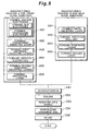
- Figs. 3 and 4 illustrate a first embodiment of a PDP according to the present invention.
- Fig. 3 is a schematic front view of the PDP in the first embodiment.
- Figs. 4A and 4B are sectional views taken along the IV-IV line in Fig. 4.
- the PDP 10 has a plurality of sustain electrode pairs (X, Y) extending in the row direction (the right-left direction in Fig. 3) and regularly arranged in the column direction (the vertical direction in Fig. 3) on the rear-facing face of a front glass substrate 1 which serves as the display surface of the PDP.
- Each of the sustain electrodes X and Y constituting a sustain electrode pair (X, Y) is composed of a bus electrodes Xa (Ya) extending in a bar shape in the row direction, and transparent electrodes Xb (Yb) which are spaced at regular intervals along the bus electrode Xa (Ya) and each extend from the bus electrode Xa (Ya) toward their counterparts in the sustain electrode pair, so that the transparent electrodes Xb and Yb face each other across a discharge gap g.
- a transparent dielectric layer 2 is formed on the rear-facing face of the front glass substrate 1 so as to cover the sustain electrode pairs (X, Y).
- First additional dielectric layers 11 are spaced at regular intervals in the row direction on the rear-facing face of the transparent dielectric layer 2. Each of the first additional dielectric layers 11 protrudes from the rear-facing face of the transparent dielectric layer 2 and extends in the column direction along a strip area opposite to approximately intermediate positions between two transparent electrodes Xb (Yb) regularly spaced in the row direction along the bus electrode Xa(Ya) in each sustain electrode X (Y).
- Each of the first additional dielectric layers 11 has a leading face 11a facing toward and parallel to the back glass substrate 5.
- An address electrode D1 extends in the column direction on the leading face 11a.
- the address electrode D1 can be formed, as illustrated in Fig. 4A, in a central portion of the leading face 11a of the first additional dielectric layer 11, namely, a position corresponding to the intermediate position between the transparent electrodes Xb (Yb) arranged in the row direction.
- the address electrode D1 is formed preferably, on the leading face 11a of the first additional dielectric layer 11, in a position shifted in the direction of the transparent electrode Yb which is to be paired with this address electrode D1 (on the left hand in Fig. 4B in the example), in order to ensure the initiation of an address discharge between the address electrode D1 and the transparent electrode Yb and prevent a false discharge between the address electrode D1 and an adjacent unrelated transparent electrode Yb.
- a second additional dielectric layer 12 is formed on and alongside the first additional dielectric layer 11 and covers the address electrode D1 formed on the leading face 11a of the first additional dielectric layer 11.
- a protective layer (not shown) formed of a high y dielectric material such as MgO is formed on the surfaces of the transparent dielectric layer 2, the first additional dielectric layers 11 and the second additional dielectric layers 12, and covers these surfaces.
- a partition wall unit 7 is formed on the white dielectric layer 6, and in an approximate grid shape of vertical walls 7A and second transverse walls 7B.
- Each of the vertical walls 7A extends in the column direction along a strip area opposite to the address electrode D1.
- Each of the transverse walls 7B extends in the row direction along a strip area opposite to the bus electrodes Xa and Ya of the back-to-back sustain electrodes X and Y of the adjacent sustain electrode pairs (X, Y) and the area between the bus electrodes Xa and Ya.
- Red-, green- and blue-colored phosphor layers 8 are each formed on five faces: the side faces of the two vertical walls 7A and the two transverse walls 7B of the partition wall unit 7 and the face of the white dielectric layer 6 surrounded by the partition wall unit 7.
- the red-, green- and blue-colored phosphor layers 8 are arranged in order in the row direction.
- the structure on the back glass substrate 5 as described above is the same as that in the conventional PDP described in Figs. 1 and 2.
- the same components are designated by the same reference numerals.
- the partition wall unit 7 partitions the discharge space defined between the front glass substrate 1 and the back glass substrate 5 into areas each corresponding to the opposing paired transparent electrodes Xb and Yb in each sustain electrode pair (X, Y), to form discharge cells C1.
- the discharge space between the front and back glass substrates 1 and 5 is filled with a discharge gas including xenon (Xe).
- the above-mentioned PDP 10 generates an image as follows.
- a reset discharge is first produced simultaneously between the sustain electrodes X and Y or between the sustain electrode Y and the address electrode D1 in all the discharge cells C1.
- the wall charge is erased from every portions of the transparent dielectric layer 2 facing the discharge cells C1 (or wall charge is accumulated on every portions of the transparent dielectric layer 2 facing the discharge cells C1).
- a scan pulse is sequentially applied to one sustain electrode (the sustain electrode Y in this example) of the sustain electrode pair (X, Y) , and a data pulse corresponding to the display data of the image signal is applied to the address electrode D1.
- a scan pulse is sequentially applied to one sustain electrode (the sustain electrode Y in this example) of the sustain electrode pair (X, Y)
- a data pulse corresponding to the display data of the image signal is applied to the address electrode D1.
- an address discharge is produced selectively in the discharge cells C1.
- the address discharge results in the deposition of wall charge on the portion of the transparent dielectric layer 2 facing each of the discharge cells C1 in which the address discharge is produced (or the erasure of the wall charge on the transparent dielectric layer 2).
- the discharge cells C1 light-emitting cells
- the discharge cells C1 non-light-emitting cells having no wall charge are distributed over the panel face.
- a sustain pulse is applied to the sustain electrodes X and Y.
- a sustain discharge is initiated across the discharge gap between the opposing transparent electrodes Xb and Yb of the sustain electrodes X and Y in each of the discharge cells C1 (light-emitting cells) having the deposition of wall charge on the transparent dielectric layer 2.
- the sustain discharge allows vacuum ultraviolet light to be generated from the xenon included in the discharge gas.
- the vacuum ultraviolet light excites the red-, green- and blue-colored phosphor layers 8 to cause them to emit color light, thereby forming an image on matrix display.
- each of the address electrodes D1 is formed on the leading face 11a of the first additional dielectric layer 11 protruding toward the back glass substrate 5 from the rear-facing face of the transparent dielectric layer 2. Because of this design, the distance between the address electrode D1 and the transparent electrode Yb of the sustain electrode Y between which an address discharge is initiated is increased as compared with that in a conventional PDP. Further, as seen from Figs. 4A and 4B, because a space is interposed between the address electrode D1 and the transparent electrode Yb of the sustain electrode Y, the electrostatic capacity between these electrodes is reduced and therefore the electrical power consumption is reduced.
- the address electrode D1 is located substantially in the thickness direction of the panel with respect to the transparent electrode Yb of the sustain electrode Y. Hence, the address discharge initiated between these electrodes is an approximate opposite discharge. This facilitates the ease of occurrence of a discharge, leading to a drop in the address discharge voltage and widening of the address voltage margin.
- Electric current typically flows when a potential difference is produced between electrodes.
- the larger the current flow the larger the electrostatic capacity between the electrodes.
- the current generated by this electrostatic capacity is reactive current.
- the first additional dielectric layer 11 causing the electrostatic capacity between the address electrode D1 and the transparent electrode Yb of the sustain electrode Y is formed of a dielectric material having a small relative dielectric constant, or alternatively the thickness of the first additional dielectric layer 11 is increased.
- the electrostatic capacity between these electrodes can be reduced by using a dielectric material having a small relative dielectric constant to form the second additional dielectric layer 12 because the second additional dielectric layer 12 is also closely involved in the occurrence of the electrostatic capacity between the address electrode D1 and the transparent electrode Yb.
- the transparent dielectric layer 2 is also closely involved in the occurrence of the electrostatic capacity between the address electrode D1 and the transparent electrode Yb, the transparent dielectric layer 2 needs to be formed of a transparent dielectric material because of its location closer to the display surface of the panel. For this reason, it is difficult to reduce the relative dielectric constant of the transparent dielectric layer 2.
- the first additional dielectric layer 11 is not required to be formed of a transparent dielectric material, as is the transparent dielectric layer 2. Hence, it is possible to reduce the relative dielectric constant of the first additional dielectric layer 11 for a reduction in electrostatic capacity.
- the relative dielectric constant of the first dielectric layer 11 is preferably set at a value falling within the range from about one to about ten.
- Fig. 5 shows a flowchart of the manufacturing process of the PDP 10.
- sustain electrodes X and Y are first formed on the rear-facing face of the front glass substrate 1 (step AS1).
- Step AS1 includes the step of forming the bus electrodes Xa and Ya of the sustain electrodes X and Y and the step of forming the transparent electrodes Xb and Yb thereof.
- a transparent dielectric layer 2 is formed on the rear-facing face of the front glass substrate 1 (step AS2), so as to cover the sustain electrode pairs (X, Y) which have been formed in step AS1.
- first additional dielectric layers 11 are formed in predetermined positions on the rear-facing face of the transparent dielectric layer 2 by a method such as pattern-printing of a dielectric paste or burning (step AS3).
- address electrodes D1 are respectively formed on the leading faces 11a of the first additional dielectric layers 11 (step AS4).
- second additional dielectric layers 12 are formed to lie on the respective first additional dielectric layers 11 (step AS5).
- the address electrodes D1 are covered by the second additional dielectric layers 12.
- step AS6 a high y dielectric material is used to form a protective layer for covering the surfaces of the transparent electrode 2, the first additional dielectric layers 11 and the second additional dielectric layers 12 (step AS6).
- a white dielectric layer 6 is first formed on the front-facing face of the back glass substrate 5 (step BS1). After the white dielectric layer 6 has been formed in step BS1, a partition wall unit 7 is formed (step BS2).
- red, green and blue phosphor layers 8 are each formed in the areas defined by the partition wall unit 7 (step BS3).
- a sealing layer is formed on the periphery edge portion of the front-facing face of the back glass substrate 5 (step BS4) .
- step CS1 The front glass substrate 1 with the various structures thus formed thereon in the manufacturing process A and the back glass substrate 5 with the various structures thus formed thereon in the manufacturing process B are placed on each other with precise alignment so as to form a discharge space between them (step CS1) . Then, the step of sealing the discharge space between the front glass substrate 1 and the back glass substrate 5 (step CS2), the step of baking and removing the gases from the discharge space (step CS3), the step of introducing a discharge gas into the discharge space (step CS4), and the step of sealing the discharge gas inside (tip-off) (step CS5) are performed in order to fabricate a PDP10.
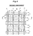
- Figs. 6, 7A and 7B illustrate a second embodiment of a PDP according to the present invention.
- Fig. 6 is a schematic front view of the PDP in the second embodiment.
- Figs. 7A and 7B are sectional views taken along the VII-VII line in Fig. 6.
- the PDP 20 has a plurality of sustain electrode pairs (X, Y) extending in the row direction (the right-left direction in Fig. 6) and regularly arranged in the column direction (the vertical direction in Fig. 6) on the rear-facing face of a front glass substrate 1 which serves as the display surface of the PDP.
- Each of the sustain electrodes X and Y constituting a sustain electrode pair (X, Y) is composed of a bus electrode Xa (Ya) extending in a bar shape in the row direction, and transparent electrodes Xb (Yb) which are spaced at regular intervals along the bus electrode Xa (Ya) and each extend from the bus electrode Xa (Ya) toward their counterparts in the sustain electrode pair, so that the transparent electrodes Xb and Yb face each other across a discharge gap g.
- a transparent dielectric layer 2 is formedon the rear-facing face of the front glass substrate 1 so as to cover the sustain electrode pairs (X, Y).
- the above structure is the same as the structure of the PDP 10 described in the first embodiment.
- the same components are designated by the same reference numerals.
- a protective layer (not shown) formed of a high y dielectric material such as MgO is formed on the rear-facing face of the transparent dielectric layer 2 and covers its surface.
- a metal grid 27a constituting the partition wall unit 27 and having a shape described later is formed integrally on a metal plate 25a constituting the back substrate 25.
- the surfaces of the metal plate 25a and the metal grid 27a are respectively covered by an insulation film 25b and an insulation film 27b.
- the partition wall unit 27 is formed substantially in a grid shape of vertical walls 27A and transverse walls 27B.
- Each of the vertical walls 27A extends in the column direction along a strip area opposite to the approximately intermediate positions between transparent electrodes Xb (Yb) regularly spaced along the associated bus electrodes Xa (Ya) of the sustain electrodes X (Y) formed on the front glass substrate 1.
- Each of the transverse walls 7B extends in the row direction along a strip area opposite to the bus electrodes Xa and Ya of the back-to-back sustain electrodes X and Y of the adjacent sustain electrode pairs (X, Y) and to the area between the bus electrodes Xa and Ya.
- Each of the vertical walls 27A of the partition wall unit 27 has a leading face 27Aa facing the front glass substrate 1, and an address electrode D2 extends in the column direction on the leading face 27Aa.
- the address electrode D2 can be formed, as illustrated in Fig. 7A, in a central portion of the leading face 27Aa of the vertical wall 27, namely, along a strip area opposite to the substantially intermediate positions between transparent electrodes Xb (Yb) regularly arranged in the row direction. However, as shown in Fig. 7B, the address electrode D2 is formed preferably, on the leading face 27Aa of the vertical wall 27, in a position shifted in the direction of the transparent electrode Yb (on the left hand in Fig.
- a dielectric cover layer 21 is formed on the leading face 27Aa of each of the vertical walls 27A and covers the address electrode D2 formed on the leading end 27Aa of the vertical wall 27.
- Red-, green- and blue-colored phosphor layers 28 are each formed on five faces: the side faces of the two vertical walls 27A and the two transverse walls 27B of the partition wall unit 27 and the face of the back substrate 25 surrounded by the partition wall unit 27.
- the red-, green- and blue-colored phosphor layers 8 are arranged in order in the row direction.
- the partition wall unit 27 partitions the discharge space defined between the front glass substrate 1 and the back substrate 25 into areas each corresponding to the opposing paired transparent electrodes Xb and Yb in each sustain electrode pair (X, Y), to form discharge cells C2.
- the discharge space between the front and back substrates 1 and 25 is filled with a discharge gas including xenon (Xe).
- the above-mentioned PDP 20 generates an image as follows.
- a reset discharge is first produced simultaneously between the sustain electrodes X and Y or between the sustain electrode Y and the address electrode D2 in all the discharge cells C2.
- the wall charge is erased from every portions of the transparent dielectric layer 2 facing the discharge cells C2 (or wall charge is accumulated on every portions of the transparent dielectric layer 2 facing the discharge cells C2).
- a scan pulse is sequentially applied to one sustain electrode (the sustain electrode Y in this example) of the sustain electrode pair (X, Y) , and a data pulse corresponding to the display data of the image signal is applied to the address electrode D2.
- a scan pulse is sequentially applied to one sustain electrode (the sustain electrode Y in this example) of the sustain electrode pair (X, Y)
- a data pulse corresponding to the display data of the image signal is applied to the address electrode D2.
- the address discharge results in the deposition of wall charge on the portion of the transparent dielectric layer 2 facing each of the discharge cells C2 in which the address discharge is produced (or the erasure of the wall charge on the transparent dielectric layer 2).
- the discharge cells C2 (light-emitting cells) each having the deposition of wall charge on the portion of the transparent dielectric layer 2 facing the discharge cell C2, and the discharge cells C2 (non-light-emitting cells) having no wall charge are distributed over the panel face.
- a sustain pulse is applied to the sustain electrodes X and Y.
- a sustain discharge is initiated across the discharge gap between the opposing transparent electrodes Xb and Yb of the sustain electrodes X and Y in each of the discharge cells C2 (light-emitting cells) having the deposition of wall charge on the transparent dielectric layer 2.
- the sustain discharge allows vacuum ultraviolet light to be generated from the xenon included in the discharge gas.
- the vacuum ultraviolet light excites the red-, green- and blue-colored phosphor layers 28 to cause them to emit color light, thereby forming an image on matrix display.
- each of the address electrodes D2 is formed on the leading face 27Aa of the vertical wall 27A of the partition wall unit 27 partitioning the discharge space into the discharge cells C2. Because of this design, the distance between the address electrode D2 and the transparent electrode Yb of the sustain electrode Y between which an address discharge is initiated is increased as compared with that in a conventional PDP. Further, as seen from Figs. 7A and 7B, because a space is interposed between the address electrode D2 and the transparent electrode Yb of the sustain electrode Y, the electrostatic capacity between these electrodes is reduced and therefore the electric power consumption is reduced.
- the address electrode D2 is located substantially in the thickness direction of the panel with respect to the transparent electrode Yb of the sustain electrode Y. Hence, the address discharge initiated between these electrodes is an approximate opposite discharge. This facilitates the ease of occurrence of a discharge, leading to a drop in the address discharge voltage and widening of the address voltage margin.
- Electric current typically flows when a potential differenceisproduced between electrodes.
- the larger the current flow the larger the electrostatic capacity between the electrodes.
- the current generated by this electrostatic capacity is reactive current.
- the PDP 20 most of the electrostatic capacity between the address electrode D2 and the transparent electrode Yb of the sustain electrode Y is produced by the transparent dielectric layer 2 and the dielectric cover layer 21 which are interposed between the address electrode D2 and the transparent electrode Yb. Accordingly, the distance between the address electrode D2 and the transparent electrode Yb is greater than that of the conventional PDP. Thereby, the electrostatic capacity is reduced in the PDP 20.
- the dielectric cover layer21 causing the electrostatic capacity between the address electrode D2 and the transparent electrode Yb of the sustain electrode Y is formed of a dielectric material having a small relative dielectric constant, or alternatively the thickness of the dielectric cover layer 21 is increased.
- the electrostatic capacity between these electrodes can be reduced by using a dielectric material having a small relative dielectric constant to form the insulation film 27b covering the metal gird 27a partially constituting the partition wall unit 27 or by increasing the thickness of the insulation film 27b because the insulation film 27b is also closely involved in the occurrence of the electrostatic capacity between the address electrode D2 and the transparent electrode Yb.
- the transparent dielectric layer 2 is also closely involved in the occurrence of the electrostatic capacity between the address electrode D2 and the transparent electrode Yb, the transparent dielectric layer 2 needs to be formed of a transparent dielectric material because of its location closer to the display surface of the panel. For this reason, it is difficult to reduce the relative dielectric constant of the transparent dielectric layer 2.
- the dielectric cover layer 21 is not required to be formed of a transparent dielectric material, as is the transparent dielectric layer 2. Hence, it is possible to reduce the relative dielectric constant of the transparent dielectric layer 2 for a reduction in electrostatic capacity.
- the relative dielectric constant of the dielectric cover layer 21 is preferably set at a value falling within the range from about one to about ten.
- the back substrate 25 and the partition wall unit 27 are previously formed integrally by the use of a metal material. Simplification of the manufacturing process is possible.
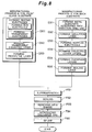
- Fig. 8 shows a flowchart of the manufacturing process of the PDP 20.
- sustain electrodes X and Y are first formed on the rear-facing face of the front glass substrate 1 (step DS1).
- Step DS1 includes the step of forming the bus electrodes Xa and Ya of the sustain electrodes X and Y and the step of forming the transparent electrodes Xb and Yb thereof.
- a transparent dielectric layer 2 is formed on the rear-facing face of the front glass substrate 1 (step DS2), so as to cover the sustain electrode pairs (X, Y) which have been formed in step DS1.
- step DS2 a high y dielectric material is used to formaprotective layer for covering the surfaces of the transparent electrode 2 (step DS3).
- a metal plate 25a and a metal grid 27a are formed integrally to form a metallic substrate (step ES1).
- insulation films 25b and 27b are formed on the surface of the metallic substrate (step ES2).
- address electrodes D2 are formed on the respective leading faces 27Aa of the vertical walls 27A of the partition wall unit 27 (step ES3).
- step ES4 dielectric cover layers 21 are formed on the respective leading faces 27Aa of the vertical walls 27A of the partition wall unit 27 (step ES4), so that the address electrodes D2 are covered by the dielectric cover layers 21.
- red, green and blue phosphor layers 28 are each formed in the areas defined by the partition wall unit 27 (step ES5). Then, a sealing layer is formed on the periphery edge portion of the front-facing face of the back substrate 25 (step ES6).
- step FS1 The front glass substrate 1 with the various structures thus formed thereon in the manufacturing process D and the back substrate 25 with the various structures thus formed thereon in the manufacturing process E are placed on each other with precise alignment so as to form a discharge space between them (step FS1) . Then, the step of sealing the discharge space between the front glass substrate 1 and the glass substrate 25 (step FS2), the step of baking and removing the gases from the discharge space (step FS3), the step of introducing a discharge gas into the discharge space (step FS4), and the step of sealing the discharge gas inside (tip-off) (step FS5) are performed in order to fabricate a PDP20.
- Fig. 9 illustrates an example of modification of the PDP 20 in the second embodiment.
- the PDP 20 has the back substrate 25 which is the metallic substrate having the partition wall unit 27 formed integrally.
- a PDP 30 in this example has a back glass substrate 35 formed of a glass substrate as in the case of the PDP 10 in the first embodiment.
- a white dielectric layer 36 is formed on the front-facing face of the back glass substrate 35.
- a partition wall unit 37 is structured as ametallicpartition wall in such a manner that an insulation film 37b covers the surface of a metal grid 37a.
- the structure of the other components is the same as those of the PDP 20.
- the same components as those in the PDP 20 are designated by the same reference numerals.
- the PDP 30 it is also possible for the PDP 30 to reduce the electric power consumption and the address discharge voltage.
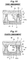
- Fig. 10 is a sectional view illustrating a third embodiment according to the present invention.
- the sectional view of Fig. 10 shows a PDP in the third embodiment taken along the same position as that of Fig. 4A of the first embodiment (the line IV-IV in Fig. 3).
- the PDP 40 has a transparent dielectric layer 2 covering sustain electrode pairs (only a transparent electrode Yb is shown in Fig. 10) which are formed on the rear-facing face of the front glass substrate 1.
- First additional dielectric layers 31 are spaced at regular intervals in the row direction on the rear-facing face of the transparent dielectric layer 2.
- Each of the first additional dielectric layers 31 projects from the rear-facing face of the transparent dielectric layer 2 and extends in the column direction along the strip area opposite to the approximately intermediate positions between two transparent electrodes arranged at regular intervals along the bus electrode of the sustain electrode.
- Each of the first additional dielectric layers 31 has a leading face 31a facing the back glass substrate 5 in parallel.
- An address electrode D3 is formed on each leading face 31a and extends in the column direction.
- the address electrode D3 is covered by a second additional dielectric layer 32 that is formed on the first dielectric layer 31.
- the address electrode D3 of the PDP 40 has a thickness a1 (the length in the direction parallel to the thickness direction of the front glass substrate 1 and the back glass substrate 5) which is set at a value equal to one-tenth or more of the width b1 (the length in the direction parallel to the front glass substrate 1 and the back glass substrate 5) and below the thickness v1 (the length in the direction parallel to the thickness direction of the front glass substrate 1 and the back glass substrate 5) of the second additional dielectric layer 32.
- the thickness a1 of the address electrode D3 is set at a value ranging from 5 ⁇ m or more to less than 15 ⁇ m.
- the effective electrode area of the address electrode D3 corresponds to the area of the side face D3a of the address electrode D3 facing the discharge cell C1.
- the address electrode D3 has a small effective electrode area, an address discharge is hard to initiate.
- the thickness a1 of the address electrode D3 is set at a value equal to one-tenth or more of the width b1, it is possible to ensure an adequate effective electrode area. Thus, an address discharge easily occurs. In addition to the technical effects described in the first embodiment, a further drop in the address discharge voltage is possible.
- the reason why the thickness a1 of the address electrode D3 is set at a value less than the thickness v1 of the second additional dielectric layer 32 is for the purpose of completely covering the address electrode D3 with the second additional dielectric layer 32.
- the thickness (in the direction parallel to the thickness direction of the front glass substrate and the back substrate) of the address electrode formed on the leading face of the vertical wall of the partition wall unit defining the discharge cells is set at a value equal to one-tenth or more of the width of the address electrode in the direction parallel to the row direction, and below the thickness (in the direction parallel to the thickness direction of the front glass substrate and the back substrate) of the dielectric cover layer covering the address electrodes.
- Fig. 11 is a sectional view illustrating a fourth embodiment according to the present invention.
- the sectional view of Fig. 11 shows a PDP in the fourth embodiment taken along the same position as that of Fig. 4A of the first embodiment (the line IV-IV in Fig. 3).
- the PDP 50 has a transparent dielectric layer 2 covering sustain electrode pairs (only a transparent electrode Yb is shown in Fig. 11) which are formed on the rear-facing face of the front glass substrate 1.
- First additional dielectric layers 41 are spaced at regular intervals in the row direction on the rear-facing face of the transparent dielectric layer 2.
- Each of the first additional dielectric layers 41 projects from the rear-facing face of the transparent dielectric layer 2 and extends in the column direction along the strip area opposite to the substantially intermediate positions between two transparent electrodes arranged at regular intervals along the bus electrode of the sustain electrode.
- Each of the first additional dielectric layers 41 has a leading face 41a facing the back glass substrate 5 in parallel.
- An address electrode D4 is formed on each leading face 41a and extends in the column direction.
- the address electrode D4 is covered by a second additional dielectric layer 42 that is formed on the first dielectric layer 41.
- the address electrode D4 of the PDP 50 has a width b2 (the length in the direction parallel to the front glass substrate 1 and the back glass substrate 5) which is set at a value equal to ten or more times the thickness a2 (the length in the direction parallel to the thickness direction of the front glass substrate 1 and the back glass substrate 5) and below the width w1 (the length in the direction parallel to the front glass substrate 1 and the back glass substrate 5) of the second additional dielectric layer 42.
- the width b2 of the address electrode D4 is set at a value ranging from 50 ⁇ m or more to less than 70 ⁇ m.
- the effective electrode area of the address electrode D4 corresponds to the area of the side face D4a of the address electrode D4 facing the discharge cell C1. Therefore, when the address electrode D4 has a small thickness a2 and a small effective electrode area, an address discharge is hard to initiate. However, in actuality, due to electric filed diffraction, a portion of the leading face D4b (i.e. the face facing parallel to the back glass substrate 5) extending continuously from the side face D4a of the address electrode D4 is involved in the address discharge d2.
- the width b2 of the address electrode D4 is set at a value equal to ten or more times the thickness a2.
- the reason why the width b2 of the address electrode D4 is set at a value less than the width w1 of the second additional dielectric layer 42 is for the purpose of completely covering the address electrode D4 with the second additional dielectric layer 42.
- the width (in the direction parallel to the row direction) of the address electrode formed on the leading face of the vertical wall of the partition wall unit defining the discharge cells is set at a value equal to ten or more times the thickness of the address electrode in the direction parallel to the thickness direction of the front glass substrate and the back substrate, and below the width (in the direction parallel to the row direction) of the dielectric cover layer covering the address electrodes.
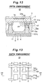
- Fig. 12 is a sectional view illustrating a fifth embodiment according to the present invention.
- the sectional view of Fig. 12 shows a PDP in the fifth embodiment taken along the same position as that of Fig. 4A of the first embodiment (the line IV-IV in Fig. 3).
- the PDP 60 has a transparent dielectric layer 2 covering sustain electrode pairs (only a transparent electrode Yb is shown in Fig. 12) which are formed on the rear-facing face of the front glass substrate 1.
- First additional dielectric layers 51 are spaced at regular intervals in the row direction on the rear-facing face of the transparent dielectric layer 2.
- Each of the first additional dielectric layers 51 projects from the rear-facing face of the transparent dielectric layer 2 and extends in the column direction along the strip area opposite to the substantially intermediate positions between two transparent electrodes arranged at regular intervals along the bus electrode of the sustain electrode.
- Each of the first additional dielectric layers 51 has a leading face 51a facing the back glass substrate 5 in parallel.
- An address electrode D5 is formed on each leading face 51a and extends in the column direction.
- the address electrode D5 is covered by a second additional dielectric layer 52 that is formed on the first dielectric layer 51.
- the second additional dielectric layer 52 of the PDP 60 has a width w2 (the length in the direction parallel to the front glass substrate 1 and the back glass substrate 5) which is set at a value equal to 4.5 or more times the width v2 (the length in the direction parallel to the thickness direction of the front glass substrate 1 and the back glass substrate 5).
- the width w2 of the second additional dielectric layer 52 is set at 67.5 ⁇ m or more, more preferably, at 70 ⁇ m or more.
- An upper limit of the width w2 of the second additional dielectric layer 52 is set at a value equal to or smaller than the width of the first additional dielectric layer 51.
- the effective electrode area of the address electrode D5 corresponds to the area of the side face D5a of the address electrode D5 facing the discharge cell C1. Therefore, when the address electrode D5 has a small thickness and a small effective electrode area, an address discharge is hard to initiate. However, if the width of the second additional dielectric layer 52 in increased, as shown in Fig. 12, this diffracts the discharge path of the address discharge d3 towards the leading face 52b (i.e. the face facing parallel to the back glass substrate 5) of the second additional dielectric layer 52. As a result, the leading face D5b of the address electrode D5 is also involved in the address discharge d3.
- the width w2 of the second additional dielectric layer 52 is set at a value equal to 4.5 times or more the thickness v2.
- an address discharge easily occurs.
- a further drop in the address discharge voltage is possible.
- the width (in the direction parallel to the row direction) of the dielectric cover layer covering the address electrode formed on the leading face of the vertical wall of the partition wall unit defining the discharge cells is set at a value equal to 4.5 or more times the thickness of the dielectric cover layer in the direction parallel to the thickness direction of the front glass substrate and the back substrate. Further, the width of the dielectric cover layer in the direction parallel to the row direction is set at a value equal to or less than the width of the vertical wall of the partition wall unit in the direction parallel to the row direction.
- Figs. 13 and 14 illustrate a sixth embodiment according to the present invention.
- Fig. 13 is a schematic front view of a PDP of the sixth embodiment.
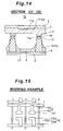
- Fig. 14 is a sectional view taken along the XIV-XIV line in Fig. 13.
- a transparent electrode Y1b of a sustain electrode Y1 out of sustain electrodes constituting each sustain electrode pair has an approximate I shape.
- a side portion Y1b1 located close to an address electrode D1 which is to be paired with the sustain electrode Y1 when an address discharge is produced extends linearly parallel to the address electrode D1.
- Figs. 13 and 14 the same components as those of the PDP in the first embodiment are designated by the same reference numerals as those in Figs. 3 and 4A.
- the side portion of Y1b1 of the transparent electrode Y1b of the sustain electrode Y1 located closer to the address electrode D1 extends linearly parallel to the address electrode D1, so that the area of the transparent electrode Y1b contributing to the address discharge is increased as compared with the case of the substantially T-shaped transparent electrode as described in the first embodiment.
- an address discharge easily occurs.
- a further drop in the address discharge voltage is possible.
- a transparent electrode Y2b of a sustain electrode Ys may be formed substantially in a L shape that a side portion Y2b1 close to the address electrode D1 for an address discharge extends linearly in parallel to the address electrode D1.
- the formation of the transparent electrode Y2b of the sustain electrode Y2 in an approximate L shape (a recess is formed in the sideportion opposite the sideportion facing toward the address electrode D1 which initiates an address discharge in conjunction with the transparent electrode Y2b) as shown in Fig. 15, means an increase in the distance between the transparent electrode Y2b and an unrelated address electrode D1 located opposite to the address electrode D1, paired with the transparent electrode Y2b for producing the address discharge, with the transparent electrode Y2 in between. This increased distance leads to prevention of a false discharge from occurring between the transparent electrode and the unrelated address electrode D1 located opposite to the address electrode D1 which is paired with the transparent electrode Y2b for producing the address discharge.
- the other sustain electrode X of the sustain electrode pair can be formed in various shapes, such as an approximate T shape as shown in Figs. 13 and 15, an approximate I shape similar to the shape of the transparent electrode Y1b of the sustain electrode Y1 shown in Fig. 13, or an approximate L shape similar to the shape of the transparent electrode Y2b of the sustain electrode Y2 shown in Fig. 15.
Landscapes
- Physics & Mathematics (AREA)
- Engineering & Computer Science (AREA)
- Plasma & Fusion (AREA)
- Gas-Filled Discharge Tubes (AREA)
Abstract
Description
- This invention relates to the panel structure of surface-discharge-type alternating-current plasma display panels.
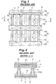
- Some surface-discharge-type alternating-current plasma displaypanels (hereinafter referred to as "PDP") have a structure, as shown in Figs. 1 and 2, in which sustain electrode pairs and address electrodes are both formed on one glass substrate of a pair of glass substrates facing each other across the discharge space.
- The PDP illustrated in Figs. 1 and 2 has sustain electrode pairs (X, Y) formed on the rear-facing face (i.e. the face facing toward the rear of the PDP) of a
front glass substrate 1 serving as the display surface of the PDP. The sustain electrode pairs (X, Y) extend in the row direction (the right-left direction in Fig. 1) and are regularly arranged in the column direction (the vertical direction in Fig. 1). - Each of the sustain electrodes X and Y constituting each sustain electrode pair (X, Y) is composed of a bus electrode Xa (Ya) extending in a bar shape in the row direction and transparent electrodes Xb (Yb) spaced at regular intervals along the bus electrode Xa (Ya) and each extending out to face the counterpart transparent electrodes Yb (Xb) with a discharge gap g in between.
- A first
dielectric layer 2 is formed on the rear-facing face of thefront glass substrate 1 so as to cover the sustain electrode pairs (X, Y). - Address electrodes D are regularly arranged in the row direction on the rear-facing face of the first
dielectric layer 2. Each of the address electrodes D extends in the column direction along a strip area opposite to the positions between two transparent electrodes Xb (Yb) regularly spaced in the row direction in each sustain electrode X (Y). The address electrodes D are covered by a seconddielectric layer 3 formed on the rear-facing face of the firstdielectric layer 2. - Additional
dielectric layers 4 project toward the rear of the PDP from the rear-facing face of the seconddielectric layer 3. Each of the additionaldielectric layers 4 extends in the column direction oppos-ite to the address electrode D. - On the rear-facing faces of the second
dielectric layer 3 and the additionaldielectric layers 4, a protective layer (not shown) formed of high y dielectrics, such as MgO, is provided. - The
front glass substrate 1 is positioned opposite to aback glass substrate 5 with a discharge space in between. A whitedielectric layer 6 is formed on the front-facing face of theback glass substrate 5. Apartition wall unit 7 is formed on the whitedielectric layer 6. Thepartition wall unit 7 is shaped substantially in a grid form ofvertical walls 7A andtransverse walls 7B. Each of thevertical walls 7A extends in the column direction opposite to the address dielectric D. Each of thetransverse walls 7B extends in the row direction along a strip area opposite to the strip area between bus electrodes Xa and Ya of the back-to-back sustain electrodes X and Y of the adjacent sustain electrode pairs (X, Y). - This
partition wall unit 7 partitions the discharge space between thefront glass substrate 1 and theback glass substrate 5 into areas each corresponding to the paired transparent electrodes Xb and Yb of each sustain electrode pair (X, Y) to form discharge cells C. - Red-, green- and blue-
colored phosphor layers 8 are formed on the side faces of thepartition wall unit 7 and the faces of thefront glass substrate 5 surrounded by thepartition wall unit 7, and arranged in order in the row direction. - The discharge space is filled with a discharge gas including xenon (Xe).
- Such a conventional PDP is disclosed in Japanese Patent Laid-open publication 2003-257321, for example.
- In the aforementioned PDP, a reset discharge is produced between the sustain electrodes X and Y or between the sustain electrode Y and the address electrode D. Then, an address discharge is produced selectively between the transparent electrode Yb of the sustain electrode Y and the address electrode D, resulting in the deposition of wall charge on the first
dielectric layer 2 and the seconddielectric layer 3 facing the discharge cell C in which the address discharge has been produced. - Under these conditions, a sustain pulse is applied alternately to the sustain electrodes X and Y in each sustain electrode pair (X, Y), to initiate a sustain discharge in the discharge cell C (light-emitting cell) having the deposition of wall charge on the first
dielectric layer 2 and the seconddielectric layer 3. - By means of the sustain discharge, vacuum ultraviolet light is emitted from the xenon in the discharge gas filling the light-emitting cell, and excites the red-,green-and blue-
colored phosphor layers 8. Thereupon, thephosphor layers 8 emit visible light, thus generating an image on a matrix display. - In the PDP structured as described above, the sustain electrode pairs (X, Y) and the address electrodes D are formed on the
front glass substrate 1. Therefore, the PDP has advantages such as ease of alignment between the substrates in the manufacturing process as compared with a PDP having sustain electrode pairs formed on one of the pair of front and back glass substrates and address electrodes formed on the other. - However, when the sustain electrode pairs and the address electrodes are formed on the same glass substrate as described earlier, as compared with the PDP having the sustain electrode pairs and the address electrodes formed separately on the two opposing glass substrates, the discharge initiated between the sustain electrode and the address electrode is approximate surface discharge and therefore the occurrence of a discharge becomes difficult. As a result, the discharge voltage tends to be raised and the address voltage margin narrowed. Further, the sustain electrode and the address electrode are positioned so close to each other that a space is not formed between them. Hence, a large electrostatic capacity is generated between the sustain and address electrodes, resulting in the problem of an increase in electric power consumption.
- An object of the present invention is to solve the problems associated with the surface-discharge-type alternating-current PDPs having sustain electrodes and address electrodes on one of the substrates as described above.
- To attain this object, according to a first feature of the present invention, there is provided a plasma display panel comprising: a front substrate and a back substrate placed opposite each other on either side of a discharge space; a plurality of row electrode pairs extending in the row direction and regularly arranged in the column direction on the rear-facing face of the front substrate; a dielectric layer formed on the rear-facing face of the front substrate and covering the row electrode pairs; a plurality of column electrodes extending in the column direction, regularly arranged in the row direction and initiating a discharge in conjunction with the row electrode in each unit light-emitting area formed in the discharge space; and a plurality of first ridged dielectric layers that protrude from the rear-facing face of the dielectric layer and extend in the column direction and are regularly arranged in the row direction, in which each of the column electrodes is formed on the first ridged dielectric layer.
- To attain the above object, according to a second feature of the present invention, there is provided a plasma display panel comprising: a front substrate and a back substrate placed opposite each other on either side of a discharge space; a plurality of row electrode pairs extending in the row direction and regularly arranged in the column direction on the rear-facing face of the front substrate; a dielectric layer formed on the rear-facing face of the front substrate and covering the row electrode pairs; a plurality of column electrodes extending in the column direction, regularly arranged in the row direction and initiating a discharge in conjunction with the row electrode in each unit light-emitting area formed in the discharge space; and a partition wall unit formed on the back substrate and extending at least in the column direction to block off the unit light-emitting areas adjacent to each other in the row direction from each other, with the column electrodes being formed on the partition wall unit.
- In a PDP according to an embodiment of the present invention, an address electrode initiating a discharge in conjunction with one sustain electrode of a sustain electrode pair is formed on the leading face of a first additional dielectric layer formed on the rear-facing face of a transparent dielectric layer in such a manner as to protrude from the rear-facing face of the transparent dielectric layer that is formed on the rear-facing face of the front glass substrate and covers the sustain electrode pairs. Alternatively, the address electrode is formed on the leading face of a partition wall unit formed on the back glass substrate.
- The plasma displaypanel in the embodiment is a plasma display panel having the address electrodes formed on the front glass substrate. The distance between each of the address electrodes and each of the sustain electrodes between which a discharge is produced is increased as compared with a conventional PDP. Further, a space is interposed between the address electrode and the sustain electrode. This makes the electrostatic capacity between the address and sustain electrodes lower to reduce the electric power consumption.
- Further, the address electrode is positioned substantially in the thickness direction of the panel with respect to the sustain electrode. Therefore, the address discharge caused between the address and sustain electrodes is an approximate opposing discharge. This facilitates the occurrence of a discharge, leading to a drop in the address discharge voltage and widening of the address voltage margin.
- These and other objects and features of the present invention will become more apparent from the following detailed description with reference to the accompanying drawings.
-
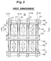
- Fig. 1 is a front view illustrating an example of the related art.
- Fig. 2 is a sectional view taken along the II-II line in Fig. 1.
- Fig. 3 is a schematic front view illustrating a first embodiment according to the present invention.
- Figs. 4A and 4B are sectional views taken along the IV-IV line in Fig. 3.
- Fig. 5 is a flowchart illustrating the manufacturing process for the plasma display panel according to the first embodiment.
- Fig. 6 is a schematic front view illustrating a second embodiment according to the present invention.
- Fig. 7 is a sectional view taken along the VII-VII line in Fig. 6.
- Fig. 8 is a flowchart illustrating the manufacturingprocess for the plasma display panel according to the second embodiment.
- Fig. 9 is a sectional view illustrating a modified example of the second embodiment.
- Fig. 10 is a sectional view illustrating a third embodiment according to the present invention.
- Fig. 11 is a sectional view illustrating a fourth embodiment according to the present invention.
- Fig. 12 is a sectional view illustrating a fifth embodiment according to the present invention.
- Fig. 13 is a schematic front view illustrating a sixth embodiment according to the present invention.
- Fig. 14 is a sectional view taken along the XIV-XIV line in Fig. 13.
- Fig. 15 is a front view illustrating a modified example of the sixth embodiment.
- Figs. 3 and 4 illustrate a first embodiment of a PDP according to the present invention. Fig. 3 is a schematic front view of the PDP in the first embodiment. Figs. 4A and 4B are sectional views taken along the IV-IV line in Fig. 4.
- In Figs. 3, 4A and 4B, the PDP 10 has a plurality of sustain electrode pairs (X, Y) extending in the row direction (the right-left direction in Fig. 3) and regularly arranged in the column direction (the vertical direction in Fig. 3) on the rear-facing face of a
front glass substrate 1 which serves as the display surface of the PDP. - Each of the sustain electrodes X and Y constituting a sustain electrode pair (X, Y) is composed of a bus electrodes Xa (Ya) extending in a bar shape in the row direction, and transparent electrodes Xb (Yb) which are spaced at regular intervals along the bus electrode Xa (Ya) and each extend from the bus electrode Xa (Ya) toward their counterparts in the sustain electrode pair, so that the transparent electrodes Xb and Yb face each other across a discharge gap g.
- A
transparent dielectric layer 2 is formed on the rear-facing face of thefront glass substrate 1 so as to cover the sustain electrode pairs (X, Y). - The above structure is the same as the structure of the conventional PDP illustrated in Figs. 1 and 2. The same components are designated by the same reference numerals.
- First additional
dielectric layers 11 are spaced at regular intervals in the row direction on the rear-facing face of thetransparent dielectric layer 2. Each of the first additionaldielectric layers 11 protrudes from the rear-facing face of thetransparent dielectric layer 2 and extends in the column direction along a strip area opposite to approximately intermediate positions between two transparent electrodes Xb (Yb) regularly spaced in the row direction along the bus electrode Xa(Ya) in each sustain electrode X (Y). - Each of the first additional
dielectric layers 11 has a leadingface 11a facing toward and parallel to theback glass substrate 5. An address electrode D1 extends in the column direction on the leadingface 11a. - In this case, the address electrode D1 can be formed, as illustrated in Fig. 4A, in a central portion of the leading
face 11a of the firstadditional dielectric layer 11, namely, a position corresponding to the intermediate position between the transparent electrodes Xb (Yb) arranged in the row direction. However, as shown in Fig. 4B, the address electrode D1 is formed preferably, on the leadingface 11a of the firstadditional dielectric layer 11, in a position shifted in the direction of the transparent electrode Yb which is to be paired with this address electrode D1 (on the left hand in Fig. 4B in the example), in order to ensure the initiation of an address discharge between the address electrode D1 and the transparent electrode Yb and prevent a false discharge between the address electrode D1 and an adjacent unrelated transparent electrode Yb. - A second
additional dielectric layer 12 is formed on and alongside the firstadditional dielectric layer 11 and covers the address electrode D1 formed on the leadingface 11a of the firstadditional dielectric layer 11. - A protective layer (not shown) formed of a high y dielectric material such as MgO is formed on the surfaces of the
transparent dielectric layer 2, the first additionaldielectric layers 11 and the second additionaldielectric layers 12, and covers these surfaces. - On the front-facing face of the
back glass substrate 5 placed opposite thefront glass substrate 1 with a discharge space in between, awhite dielectric layer 6 is formed. Apartition wall unit 7 is formed on thewhite dielectric layer 6, and in an approximate grid shape ofvertical walls 7A and secondtransverse walls 7B. Each of thevertical walls 7A extends in the column direction along a strip area opposite to the address electrode D1. Each of thetransverse walls 7B extends in the row direction along a strip area opposite to the bus electrodes Xa and Ya of the back-to-back sustain electrodes X and Y of the adjacent sustain electrode pairs (X, Y) and the area between the bus electrodes Xa and Ya. - Red-, green- and blue-
colored phosphor layers 8 are each formed on five faces: the side faces of the twovertical walls 7A and the twotransverse walls 7B of thepartition wall unit 7 and the face of thewhite dielectric layer 6 surrounded by thepartition wall unit 7. The red-, green- and blue-colored phosphor layers 8 are arranged in order in the row direction. - The structure on the
back glass substrate 5 as described above is the same as that in the conventional PDP described in Figs. 1 and 2. The same components are designated by the same reference numerals. - The
partition wall unit 7 partitions the discharge space defined between thefront glass substrate 1 and theback glass substrate 5 into areas each corresponding to the opposing paired transparent electrodes Xb and Yb in each sustain electrode pair (X, Y), to form discharge cells C1. - The discharge space between the front and back
glass substrates - The above-mentioned PDP 10 generates an image as follows.
- A reset discharge is first produced simultaneously between the sustain electrodes X and Y or between the sustain electrode Y and the address electrode D1 in all the discharge cells C1. As a result, the wall charge is erased from every portions of the
transparent dielectric layer 2 facing the discharge cells C1 (or wall charge is accumulated on every portions of thetransparent dielectric layer 2 facing the discharge cells C1). - Then, a scan pulse is sequentially applied to one sustain electrode (the sustain electrode Y in this example) of the sustain electrode pair (X, Y) , and a data pulse corresponding to the display data of the image signal is applied to the address electrode D1. Thereupon, between the address electrode D1 to which the data pulse is applied and the transparent electrode Yb of the sustain electrode Y paired with this address electrode D1, an address discharge is produced selectively in the discharge cells C1.
- The address discharge results in the deposition of wall charge on the portion of the
transparent dielectric layer 2 facing each of the discharge cells C1 in which the address discharge is produced (or the erasure of the wall charge on the transparent dielectric layer 2). Thus, the discharge cells C1 (light-emitting cells) each having the deposition of wall charge on the portion of thetransparent dielectric layer 2 facing the discharge cell C1, and the discharge cells C1 (non-light-emitting cells) having no wall charge are distributed over the panel face. - Following that, a sustain pulse is applied to the sustain electrodes X and Y. Thereupon, a sustain discharge is initiated across the discharge gap between the opposing transparent electrodes Xb and Yb of the sustain electrodes X and Y in each of the discharge cells C1 (light-emitting cells) having the deposition of wall charge on the
transparent dielectric layer 2. - In each of the discharge cells (light-emitting cells) C1, the sustain discharge allows vacuum ultraviolet light to be generated from the xenon included in the discharge gas. The vacuum ultraviolet light excites the red-, green- and blue-
colored phosphor layers 8 to cause them to emit color light, thereby forming an image on matrix display. - In the PDP 10, each of the address electrodes D1 is formed on the leading
face 11a of the firstadditional dielectric layer 11 protruding toward theback glass substrate 5 from the rear-facing face of thetransparent dielectric layer 2. Because of this design, the distance between the address electrode D1 and the transparent electrode Yb of the sustain electrode Y between which an address discharge is initiated is increased as compared with that in a conventional PDP. Further, as seen from Figs. 4A and 4B, because a space is interposed between the address electrode D1 and the transparent electrode Yb of the sustain electrode Y, the electrostatic capacity between these electrodes is reduced and therefore the electrical power consumption is reduced. - Further, the address electrode D1 is located substantially in the thickness direction of the panel with respect to the transparent electrode Yb of the sustain electrode Y. Hence, the address discharge initiated between these electrodes is an approximate opposite discharge. This facilitates the ease of occurrence of a discharge, leading to a drop in the address discharge voltage and widening of the address voltage margin.
- The following are the reasons why the electrostatic capacity between the address electrode D1 and the transparent electrode Yb of the sustain electrode Y is reduced and the electric power consumption is reduced in the PDP 10.
- Electric current typically flows when a potential difference is produced between electrodes. The larger the current flow, the larger the electrostatic capacity between the electrodes. In the PDP, the current generated by this electrostatic capacity is reactive current.
- In the conventional PDP in Fig. 2, most of the electrostatic capacity between the address electrode D and the transparent electrode Yb of the sustain electrode Y is produced by the first
dielectric layer 2 interposed between the address electrode D and the transparent electrode Yb. The distance between the address electrode D and the transparent electrode Yb is short. Thereby, the electrostatic capacity is increased. - However, in the PDP 10, most of the electrostatic capacity between the address electrode D1 and the transparent electrode Yb of the sustain electrode Y is produced by the
transparent dielectric layer 2 and the firstadditional dielectric layer 11 which are interposed between the address electrode D1 and the transparent electrode Yb. Therefore, the distance between the address electrode D1 and the transparent electrode Yb is greater than that of the conventional PDP. Thereby, the electrostatic capacity is reduced in the PDP 10. - From the foregoing, it is possible to further reduce the electrostatic capacity between the address electrode D1 and the transparent electrode Yb if the first
additional dielectric layer 11 causing the electrostatic capacity between the address electrode D1 and the transparent electrode Yb of the sustain electrode Y is formed of a dielectric material having a small relative dielectric constant, or alternatively the thickness of the firstadditional dielectric layer 11 is increased. - Further, the electrostatic capacity between these electrodes can be reduced by using a dielectric material having a small relative dielectric constant to form the second
additional dielectric layer 12 because the secondadditional dielectric layer 12 is also closely involved in the occurrence of the electrostatic capacity between the address electrode D1 and the transparent electrode Yb. - Although the
transparent dielectric layer 2 is also closely involved in the occurrence of the electrostatic capacity between the address electrode D1 and the transparent electrode Yb, thetransparent dielectric layer 2 needs to be formed of a transparent dielectric material because of its location closer to the display surface of the panel. For this reason, it is difficult to reduce the relative dielectric constant of thetransparent dielectric layer 2. - The first
additional dielectric layer 11 is not required to be formed of a transparent dielectric material, as is thetransparent dielectric layer 2. Hence, it is possible to reduce the relative dielectric constant of the firstadditional dielectric layer 11 for a reduction in electrostatic capacity. - For example, when the
transparent dielectric layer 2 has a relative dielectric constant of around ten, the relative dielectric constant of thefirst dielectric layer 11 is preferably set at a value falling within the range from about one to about ten. - Fig. 5 shows a flowchart of the manufacturing process of the PDP 10.
- Next, the manufacturing process for the PDP 10 will be described with reference to Fig. 5.
- In the manufacturing process A for the
front glass substrate 1, sustain electrodes X and Y are first formed on the rear-facing face of the front glass substrate 1 (step AS1). - Step AS1 includes the step of forming the bus electrodes Xa and Ya of the sustain electrodes X and Y and the step of forming the transparent electrodes Xb and Yb thereof.
- After the sustain electrode pairs (X, Y) have been formed in step AS1, a
transparent dielectric layer 2 is formed on the rear-facing face of the front glass substrate 1 (step AS2), so as to cover the sustain electrode pairs (X, Y) which have been formed in step AS1. - After step AS2, first additional
dielectric layers 11 are formed in predetermined positions on the rear-facing face of thetransparent dielectric layer 2 by a method such as pattern-printing of a dielectric paste or burning (step AS3). - After the first additional
dielectric layers 11 have been formed in step AS3, address electrodes D1 are respectively formed on the leadingfaces 11a of the first additional dielectric layers 11 (step AS4). - After the address electrodes D1 have been formed on the respective leading faces 11a of the first additional
dielectric layers 11 in step AS4, second additionaldielectric layers 12 are formed to lie on the respective first additional dielectric layers 11 (step AS5). The address electrodes D1 are covered by the second additional dielectric layers 12. - After the completion of step AS 5, a high y dielectric material is used to form a protective layer for covering the surfaces of the
transparent electrode 2, the first additionaldielectric layers 11 and the second additional dielectric layers 12 (step AS6). - In the manufacturing process B for the
back glass substrate 5, awhite dielectric layer 6 is first formed on the front-facing face of the back glass substrate 5 (step BS1). After thewhite dielectric layer 6 has been formed in step BS1, apartition wall unit 7 is formed (step BS2). - Then, after the
partition wall unit 7 has been formed in step BS2, red, green andblue phosphor layers 8 are each formed in the areas defined by the partition wall unit 7 (step BS3). Then, a sealing layer is formed on the periphery edge portion of the front-facing face of the back glass substrate 5 (step BS4) . - The
front glass substrate 1 with the various structures thus formed thereon in the manufacturing process A and theback glass substrate 5 with the various structures thus formed thereon in the manufacturing process B are placed on each other with precise alignment so as to form a discharge space between them (step CS1) . Then, the step of sealing the discharge space between thefront glass substrate 1 and the back glass substrate 5 (step CS2), the step of baking and removing the gases from the discharge space (step CS3), the step of introducing a discharge gas into the discharge space (step CS4), and the step of sealing the discharge gas inside (tip-off) (step CS5) are performed in order to fabricate a PDP10. - Figs. 6, 7A and 7B illustrate a second embodiment of a PDP according to the present invention. Fig. 6 is a schematic front view of the PDP in the second embodiment. Figs. 7A and 7B are sectional views taken along the VII-VII line in Fig. 6.
- In Figs. 6, 7A and 7B, the
PDP 20 has a plurality of sustain electrode pairs (X, Y) extending in the row direction (the right-left direction in Fig. 6) and regularly arranged in the column direction (the vertical direction in Fig. 6) on the rear-facing face of afront glass substrate 1 which serves as the display surface of the PDP. - Each of the sustain electrodes X and Y constituting a sustain electrode pair (X, Y) is composed of a bus electrode Xa (Ya) extending in a bar shape in the row direction, and transparent electrodes Xb (Yb) which are spaced at regular intervals along the bus electrode Xa (Ya) and each extend from the bus electrode Xa (Ya) toward their counterparts in the sustain electrode pair, so that the transparent electrodes Xb and Yb face each other across a discharge gap g.
- A
transparent dielectric layer 2 is formedon the rear-facing face of thefront glass substrate 1 so as to cover the sustain electrode pairs (X, Y). - The above structure is the same as the structure of the PDP 10 described in the first embodiment. The same components are designated by the same reference numerals.
- A protective layer (not shown) formed of a high y dielectric material such as MgO is formed on the rear-facing face of the
transparent dielectric layer 2 and covers its surface. - A
back substrate 25, which is placed opposite thefront glass substrate 1 with a discharge space in between, is formed integrally with apartition wall unit 27 by the use of a metal material. - More specifically, for the
back substrate 25 and thepartition wall unit 27, ametal grid 27a constituting thepartition wall unit 27 and having a shape described later is formed integrally on ametal plate 25a constituting theback substrate 25. The surfaces of themetal plate 25a and themetal grid 27a are respectively covered by aninsulation film 25b and aninsulation film 27b. - The
partition wall unit 27 is formed substantially in a grid shape ofvertical walls 27A andtransverse walls 27B. Each of thevertical walls 27A extends in the column direction along a strip area opposite to the approximately intermediate positions between transparent electrodes Xb (Yb) regularly spaced along the associated bus electrodes Xa (Ya) of the sustain electrodes X (Y) formed on thefront glass substrate 1. Each of thetransverse walls 7B extends in the row direction along a strip area opposite to the bus electrodes Xa and Ya of the back-to-back sustain electrodes X and Y of the adjacent sustain electrode pairs (X, Y) and to the area between the bus electrodes Xa and Ya. - Each of the
vertical walls 27A of thepartition wall unit 27 has a leading face 27Aa facing thefront glass substrate 1, and an address electrode D2 extends in the column direction on the leading face 27Aa. - The address electrode D2 can be formed, as illustrated in Fig. 7A, in a central portion of the leading face 27Aa of the
vertical wall 27, namely, along a strip area opposite to the substantially intermediate positions between transparent electrodes Xb (Yb) regularly arranged in the row direction. However, as shown in Fig. 7B, the address electrode D2 is formed preferably, on the leading face 27Aa of thevertical wall 27, in a position shifted in the direction of the transparent electrode Yb (on the left hand in Fig. 7B in the example), in order to ensure the initiation of an address discharge between the address electrode D2 and the transparent electrode Yb which is to be paired with this address electrode D2 as described later, and to prevent a false discharge between the address electrode D2 and an adjacent unrelated transparent electrode Yb. - A
dielectric cover layer 21 is formed on the leading face 27Aa of each of thevertical walls 27A and covers the address electrode D2 formed on the leading end 27Aa of thevertical wall 27. - Red-, green- and blue-colored phosphor layers 28 are each formed on five faces: the side faces of the two
vertical walls 27A and the twotransverse walls 27B of thepartition wall unit 27 and the face of theback substrate 25 surrounded by thepartition wall unit 27. The red-, green- and blue-colored phosphor layers 8 are arranged in order in the row direction. - The
partition wall unit 27 partitions the discharge space defined between thefront glass substrate 1 and theback substrate 25 into areas each corresponding to the opposing paired transparent electrodes Xb and Yb in each sustain electrode pair (X, Y), to form discharge cells C2. - The discharge space between the front and
back substrates - The above-mentioned
PDP 20 generates an image as follows. - A reset discharge is first produced simultaneously between the sustain electrodes X and Y or between the sustain electrode Y and the address electrode D2 in all the discharge cells C2. As a result, the wall charge is erased from every portions of the
transparent dielectric layer 2 facing the discharge cells C2 (or wall charge is accumulated on every portions of thetransparent dielectric layer 2 facing the discharge cells C2). - Then, a scan pulse is sequentially applied to one sustain electrode (the sustain electrode Y in this example) of the sustain electrode pair (X, Y) , and a data pulse corresponding to the display data of the image signal is applied to the address electrode D2. Thereupon, between the address electrode D2 to which the data pulse is applied and the transparent electrode Yb of the sustain electrode Y paired with this address electrode D2, an address discharge is produced selectively in the discharge cells C2.
- The address discharge results in the deposition of wall charge on the portion of the
transparent dielectric layer 2 facing each of the discharge cells C2 in which the address discharge is produced (or the erasure of the wall charge on the transparent dielectric layer 2). Thus, the discharge cells C2 (light-emitting cells) each having the deposition of wall charge on the portion of thetransparent dielectric layer 2 facing the discharge cell C2, and the discharge cells C2 (non-light-emitting cells) having no wall charge are distributed over the panel face. - Following that, a sustain pulse is applied to the sustain electrodes X and Y. Thereupon, a sustain discharge is initiated across the discharge gap between the opposing transparent electrodes Xb and Yb of the sustain electrodes X and Y in each of the discharge cells C2 (light-emitting cells) having the deposition of wall charge on the
transparent dielectric layer 2. - In each of the discharge cells (light-emitting cells) C2, the sustain discharge allows vacuum ultraviolet light to be generated from the xenon included in the discharge gas. The vacuum ultraviolet light excites the red-, green- and blue-colored phosphor layers 28 to cause them to emit color light, thereby forming an image on matrix display.
- In the
PDP 20, each of the address electrodes D2 is formed on the leading face 27Aa of thevertical wall 27A of thepartition wall unit 27 partitioning the discharge space into the discharge cells C2. Because of this design, the distance between the address electrode D2 and the transparent electrode Yb of the sustain electrode Y between which an address discharge is initiated is increased as compared with that in a conventional PDP. Further, as seen from Figs. 7A and 7B, because a space is interposed between the address electrode D2 and the transparent electrode Yb of the sustain electrode Y, the electrostatic capacity between these electrodes is reduced and therefore the electric power consumption is reduced. - Further, the address electrode D2 is located substantially in the thickness direction of the panel with respect to the transparent electrode Yb of the sustain electrode Y. Hence, the address discharge initiated between these electrodes is an approximate opposite discharge. This facilitates the ease of occurrence of a discharge, leading to a drop in the address discharge voltage and widening of the address voltage margin.
- The following are the reasons why the electrostatic capacity between the address electrode D2 and the transparent electrode Yb of the sustain electrode Y is reduced and the electric power consumption is reduced in the
PDP 20. - Electric current typically flows when a potential differenceisproduced between electrodes. The larger the current flow, the larger the electrostatic capacity between the electrodes. In the PDP, the current generated by this electrostatic capacity is reactive current.
- In the conventional PDP in Fig. 2, most of the electrostatic capacity between the address electrode D and the transparent electrode Yb of the sustain electrode Y is produced by the first
dielectric layer 2 interposed between the address electrode D and the transparent electrode Yb. The distance between the address electrode D and the transparent electrode Yb is short. Thereby, the electrostatic capacity is increased. - However, in the
PDP 20, most of the electrostatic capacity between the address electrode D2 and the transparent electrode Yb of the sustain electrode Y is produced by thetransparent dielectric layer 2 and thedielectric cover layer 21 which are interposed between the address electrode D2 and the transparent electrode Yb. Accordingly, the distance between the address electrode D2 and the transparent electrode Yb is greater than that of the conventional PDP. Thereby, the electrostatic capacity is reduced in thePDP 20. - From the foregoing, it is possible to further reduce the electrostatic capacity between the address electrode D2 and the transparent electrode Yb if the dielectric cover layer21 causing the electrostatic capacity between the address electrode D2 and the transparent electrode Yb of the sustain electrode Y is formed of a dielectric material having a small relative dielectric constant, or alternatively the thickness of the
dielectric cover layer 21 is increased. - Further, the electrostatic capacity between these electrodes can be reduced by using a dielectric material having a small relative dielectric constant to form the
insulation film 27b covering themetal gird 27a partially constituting thepartition wall unit 27 or by increasing the thickness of theinsulation film 27b because theinsulation film 27b is also closely involved in the occurrence of the electrostatic capacity between the address electrode D2 and the transparent electrode Yb. - Although the
transparent dielectric layer 2 is also closely involved in the occurrence of the electrostatic capacity between the address electrode D2 and the transparent electrode Yb, thetransparent dielectric layer 2 needs to be formed of a transparent dielectric material because of its location closer to the display surface of the panel. For this reason, it is difficult to reduce the relative dielectric constant of thetransparent dielectric layer 2. - The
dielectric cover layer 21 is not required to be formed of a transparent dielectric material, as is thetransparent dielectric layer 2. Hence, it is possible to reduce the relative dielectric constant of thetransparent dielectric layer 2 for a reduction in electrostatic capacity. - For example, when the
transparent dielectric layer 2 has a relative dielectric constant of around ten, the relative dielectric constant of thedielectric cover layer 21 is preferably set at a value falling within the range from about one to about ten. - In the foregoing
PDP 20, theback substrate 25 and thepartition wall unit 27 are previously formed integrally by the use of a metal material. Simplification of the manufacturing process is possible. - Fig. 8 shows a flowchart of the manufacturing process of the
PDP 20. - Next, the manufacturing process for the
PDP 20 will be described with reference to Fig. 8. - In the manufacturing process D for the
front glass substrate 1, sustain electrodes X and Y are first formed on the rear-facing face of the front glass substrate 1 (step DS1). - Step DS1 includes the step of forming the bus electrodes Xa and Ya of the sustain electrodes X and Y and the step of forming the transparent electrodes Xb and Yb thereof.
- After the sustain electrode pairs (X, Y) have been formed in step DS1, a
transparent dielectric layer 2 is formed on the rear-facing face of the front glass substrate 1 (step DS2), so as to cover the sustain electrode pairs (X, Y) which have been formed in step DS1. - After step DS2, a high y dielectric material is used to formaprotective layer for covering the surfaces of the transparent electrode 2 (step DS3).
- In the manufacturing process E for the
back substrate 25, ametal plate 25a and ametal grid 27a are formed integrally to form a metallic substrate (step ES1). After the metallic substrate has been formed in step ES1,insulation films - After the
back substrate 25 and thepartition wall unit 27 have been integrally formed in steps ES1 and ES2, address electrodes D2 are formed on the respective leading faces 27Aa of thevertical walls 27A of the partition wall unit 27 (step ES3). - After the address electrodes D2 have been formed in step ES3, dielectric cover layers 21 are formed on the respective leading faces 27Aa of the
vertical walls 27A of the partition wall unit 27 (step ES4), so that the address electrodes D2 are covered by the dielectric cover layers 21. - Then, red, green and blue phosphor layers 28 are each formed in the areas defined by the partition wall unit 27 (step ES5). Then, a sealing layer is formed on the periphery edge portion of the front-facing face of the back substrate 25 (step ES6).
- The
front glass substrate 1 with the various structures thus formed thereon in the manufacturing process D and theback substrate 25 with the various structures thus formed thereon in the manufacturing process E are placed on each other with precise alignment so as to form a discharge space between them (step FS1) . Then, the step of sealing the discharge space between thefront glass substrate 1 and the glass substrate 25 (step FS2), the step of baking and removing the gases from the discharge space (step FS3), the step of introducing a discharge gas into the discharge space (step FS4), and the step of sealing the discharge gas inside (tip-off) (step FS5) are performed in order to fabricate a PDP20. - Fig. 9 illustrates an example of modification of the
PDP 20 in the second embodiment. ThePDP 20 has theback substrate 25 which is the metallic substrate having thepartition wall unit 27 formed integrally. APDP 30 in this example has aback glass substrate 35 formed of a glass substrate as in the case of the PDP 10 in the first embodiment. Awhite dielectric layer 36 is formed on the front-facing face of theback glass substrate 35. - A
partition wall unit 37 is structured as ametallicpartition wall in such a manner that aninsulation film 37b covers the surface of ametal grid 37a. - The structure of the other components is the same as those of the
PDP 20. The same components as those in thePDP 20 are designated by the same reference numerals. - As in the case of the
PDP 20, it is also possible for thePDP 30 to reduce the electric power consumption and the address discharge voltage. - Fig. 10 is a sectional view illustrating a third embodiment according to the present invention. The sectional view of Fig. 10 shows a PDP in the third embodiment taken along the same position as that of Fig. 4A of the first embodiment (the line IV-IV in Fig. 3).
- As in the case of the PDP in the first embodiment, in Fig. 10, the
PDP 40 has atransparent dielectric layer 2 covering sustain electrode pairs (only a transparent electrode Yb is shown in Fig. 10) which are formed on the rear-facing face of thefront glass substrate 1. First additionaldielectric layers 31 are spaced at regular intervals in the row direction on the rear-facing face of thetransparent dielectric layer 2. Each of the first additionaldielectric layers 31 projects from the rear-facing face of thetransparent dielectric layer 2 and extends in the column direction along the strip area opposite to the approximately intermediate positions between two transparent electrodes arranged at regular intervals along the bus electrode of the sustain electrode. - Each of the first additional
dielectric layers 31 has a leadingface 31a facing theback glass substrate 5 in parallel. An address electrode D3 is formed on each leadingface 31a and extends in the column direction. The address electrode D3 is covered by a secondadditional dielectric layer 32 that is formed on thefirst dielectric layer 31. - The address electrode D3 of the
PDP 40 has a thickness a1 (the length in the direction parallel to the thickness direction of thefront glass substrate 1 and the back glass substrate 5) which is set at a value equal to one-tenth or more of the width b1 (the length in the direction parallel to thefront glass substrate 1 and the back glass substrate 5) and below the thickness v1 (the length in the direction parallel to the thickness direction of thefront glass substrate 1 and the back glass substrate 5) of the secondadditional dielectric layer 32. - For example, in the case when the PDP is of around 50-inch diagonal, when the width b1 of the address electrode D3 is set at 50µm and the thickness v1 of the second
additional dielectric layer 32 is set at 15µm, the thickness a1 of the address electrode D3 is set at a value ranging from 5µm or more to less than 15µm. - The structure of the other components is the same as those in the first embodiment. In Fig. 10, the same components as those of the PDP in the first embodiment are designated by the same reference numerals as those in Figs. 3 and 4A.
- When the dimensions of the address electrode D3 are determined in this manner, the following technical effects are exerted.
- More specifically, as shown in Fig. 10, when an address discharge d1 is produced between the address electrode D3 and the transparent electrode Yb, the effective electrode area of the address electrode D3 (i.e. the area of the electrode involved in the discharge) corresponds to the area of the side face D3a of the address electrode D3 facing the discharge cell C1.
- Therefore, when the address electrode D3 has a small effective electrode area, an address discharge is hard to initiate. In the
PDP 40, because the thickness a1 of the address electrode D3 is set at a value equal to one-tenth or more of the width b1, it is possible to ensure an adequate effective electrode area. Thus, an address discharge easily occurs. In addition to the technical effects described in the first embodiment, a further drop in the address discharge voltage is possible. - In the foregoing, the reason why the thickness a1 of the address electrode D3 is set at a value less than the thickness v1 of the second
additional dielectric layer 32 is for the purpose of completely covering the address electrode D3 with the secondadditional dielectric layer 32. - The foregoing has described the case when the dimensions of the address electrode are determined in the PDP having the same structure of that of the PDP of the first embodiment. In a like manner, the dimensions of an address electrode in a PDP of the same structure as that in the PDP in the second embodiment can be determined.
- More specifically, in a PDP of the same structure as that in the second embodiment, the thickness (in the direction parallel to the thickness direction of the front glass substrate and the back substrate) of the address electrode formed on the leading face of the vertical wall of the partition wall unit defining the discharge cells is set at a value equal to one-tenth or more of the width of the address electrode in the direction parallel to the row direction, and below the thickness (in the direction parallel to the thickness direction of the front glass substrate and the back substrate) of the dielectric cover layer covering the address electrodes. Thus, similarly, an address discharge is easy to initiate and the address discharge voltage is further reduced.
- Fig. 11 is a sectional view illustrating a fourth embodiment according to the present invention. The sectional view of Fig. 11 shows a PDP in the fourth embodiment taken along the same position as that of Fig. 4A of the first embodiment (the line IV-IV in Fig. 3).
- As in the case of the PDP in the first embodiment, in Fig. 11, the
PDP 50 has atransparent dielectric layer 2 covering sustain electrode pairs (only a transparent electrode Yb is shown in Fig. 11) which are formed on the rear-facing face of thefront glass substrate 1. First additionaldielectric layers 41 are spaced at regular intervals in the row direction on the rear-facing face of thetransparent dielectric layer 2. Each of the first additionaldielectric layers 41 projects from the rear-facing face of thetransparent dielectric layer 2 and extends in the column direction along the strip area opposite to the substantially intermediate positions between two transparent electrodes arranged at regular intervals along the bus electrode of the sustain electrode. - Each of the first additional
dielectric layers 41 has a leadingface 41a facing theback glass substrate 5 in parallel. An address electrode D4 is formed on each leadingface 41a and extends in the column direction. The address electrode D4 is covered by a secondadditional dielectric layer 42 that is formed on thefirst dielectric layer 41. - The address electrode D4 of the
PDP 50 has a width b2 (the length in the direction parallel to thefront glass substrate 1 and the back glass substrate 5) which is set at a value equal to ten or more times the thickness a2 (the length in the direction parallel to the thickness direction of thefront glass substrate 1 and the back glass substrate 5) and below the width w1 (the length in the direction parallel to thefront glass substrate 1 and the back glass substrate 5) of the secondadditional dielectric layer 42. - For example, in the case where the PDP is of around 50-inch diagonal, when the thickness a2 of the address electrode D4 is set at 5µm and the width w1 of the second
additional dielectric layer 42 is set at 70µm, the width b2 of the address electrode D4 is set at a value ranging from 50µm or more to less than 70µm. - The structure of the other components is thee same as those in the first embodiment. In Fig. 11, the same components as those of the PDP in the first embodiment are designated by the same reference numerals as those in Figs. 3 and 4A.
- When the dimensions of the address electrode D4 are determined in this manner, the following technical effects are exerted.
- More specifically, when an address discharge d2 is produced between the address electrode D4 and the transparent electrode Yb, the effective electrode area of the address electrode D4 (i.e. the area of the electrode involved in the discharge) corresponds to the area of the side face D4a of the address electrode D4 facing the discharge cell C1. Therefore, when the address electrode D4 has a small thickness a2 and a small effective electrode area, an address discharge is hard to initiate. However, in actuality, due to electric filed diffraction, a portion of the leading face D4b (i.e. the face facing parallel to the back glass substrate 5) extending continuously from the side face D4a of the address electrode D4 is involved in the address discharge d2.
- Therefore, in the
PDP 50, in order to substantially enlarge the effective electrode area of the address electrode D4, the width b2 of the address electrode D4 is set at a value equal to ten or more times the thickness a2. Thus, an address discharge easily occurs. In addition to the technical effects described in the first embodiment, a further drop in the address discharge voltage is possible. - In the foregoing, the reason why the width b2 of the address electrode D4 is set at a value less than the width w1 of the second
additional dielectric layer 42 is for the purpose of completely covering the address electrode D4 with the secondadditional dielectric layer 42. - The foregoing has described the case when the dimensions of the address electrode are determined in the PDP having the same structure of that of the PDP of the first embodiment. In a like manner, the dimensions of an address electrode in a PDP of the same structure as that in the PDP in the second embodiment can be determined.
- More specifically, in a PDP of the same structure as that in the second embodiment, the width (in the direction parallel to the row direction) of the address electrode formed on the leading face of the vertical wall of the partition wall unit defining the discharge cells is set at a value equal to ten or more times the thickness of the address electrode in the direction parallel to the thickness direction of the front glass substrate and the back substrate, and below the width (in the direction parallel to the row direction) of the dielectric cover layer covering the address electrodes. Thus, similarly, an address discharge is easy to initiate and the address discharge voltage is further reduced.
- Fig. 12 is a sectional view illustrating a fifth embodiment according to the present invention. The sectional view of Fig. 12 shows a PDP in the fifth embodiment taken along the same position as that of Fig. 4A of the first embodiment (the line IV-IV in Fig. 3).
- As in the case of the PDP in the first embodiment, in Fig. 12, the
PDP 60 has atransparent dielectric layer 2 covering sustain electrode pairs (only a transparent electrode Yb is shown in Fig. 12) which are formed on the rear-facing face of thefront glass substrate 1. First additionaldielectric layers 51 are spaced at regular intervals in the row direction on the rear-facing face of thetransparent dielectric layer 2. Each of the first additionaldielectric layers 51 projects from the rear-facing face of thetransparent dielectric layer 2 and extends in the column direction along the strip area opposite to the substantially intermediate positions between two transparent electrodes arranged at regular intervals along the bus electrode of the sustain electrode. - Each of the first additional
dielectric layers 51 has a leadingface 51a facing theback glass substrate 5 in parallel. An address electrode D5 is formed on each leadingface 51a and extends in the column direction. The address electrode D5 is covered by a secondadditional dielectric layer 52 that is formed on thefirst dielectric layer 51. - The second
additional dielectric layer 52 of thePDP 60 has a width w2 (the length in the direction parallel to thefront glass substrate 1 and the back glass substrate 5) which is set at a value equal to 4.5 or more times the width v2 (the length in the direction parallel to the thickness direction of thefront glass substrate 1 and the back glass substrate 5). - For example, in the case where the PDP is of around 50-inch diagonal, when the thickness v2 of the second
additional dielectric layer 52 is set at 15µm, the width w2 of the secondadditional dielectric layer 52 is set at 67.5µm or more, more preferably, at 70µm or more. - An upper limit of the width w2 of the second
additional dielectric layer 52 is set at a value equal to or smaller than the width of the firstadditional dielectric layer 51. - This is because, if the width w2 of the second
additional dielectric layer 52 is wider than the width of the firstadditional dielectric layer 51, stable formation of the secondadditional dielectric layer 52 is impossible from a structure viewpoint. - The structure of the other components is the same as those in the first embodiment. In Fig. 12, the same components as those of the PDP in the first embodiment are designated by the same reference numerals as those in Figs. 3 and 4A.
- When the dimensions of the second
additional dielectric layer 52 are determined in this manner, the following technical effects are exerted. - More specifically, when an address discharge d3 is produced between the address electrode D5 and the transparent electrode Yb, the effective electrode area of the address electrode D5 (i.e. the area of the electrode involved in the discharge) corresponds to the area of the side face D5a of the address electrode D5 facing the discharge cell C1. Therefore, when the address electrode D5 has a small thickness and a small effective electrode area, an address discharge is hard to initiate. However, if the width of the second
additional dielectric layer 52 in increased, as shown in Fig. 12, this diffracts the discharge path of the address discharge d3 towards the leading face 52b (i.e. the face facing parallel to the back glass substrate 5) of the secondadditional dielectric layer 52. As a result, the leading face D5b of the address electrode D5 is also involved in the address discharge d3. - Therefore, in the
PDP 60, in order to substantially enlarge the effective electrode area of the address electrode D5, the width w2 of the secondadditional dielectric layer 52 is set at a value equal to 4.5 times or more the thickness v2. Thus, an address discharge easily occurs. In addition to the technical effects described in the first embodiment, a further drop in the address discharge voltage is possible. - The foregoing has described the case when the dimensions of the second additional dielectric layer are determined in the PDP having the same structure of that of the PDP of the first embodiment. In a like manner, the dimensions of a second additional dielectric layer in a PDP of the same structure as that in the PDP in the second embodiment can be determined.
- More specifically, in a PDP of the same structure as that in the second embodiment, the width (in the direction parallel to the row direction) of the dielectric cover layer covering the address electrode formed on the leading face of the vertical wall of the partition wall unit defining the discharge cells is set at a value equal to 4.5 or more times the thickness of the dielectric cover layer in the direction parallel to the thickness direction of the front glass substrate and the back substrate. Further, the width of the dielectric cover layer in the direction parallel to the row direction is set at a value equal to or less than the width of the vertical wall of the partition wall unit in the direction parallel to the row direction. Thus, similarly, an address discharge is easy to initiate and the address discharge voltage is further reduced.
- Figs. 13 and 14 illustrate a sixth embodiment according to the present invention. Fig. 13 is a schematic front view of a PDP of the sixth embodiment. Fig. 14 is a sectional view taken along the XIV-XIV line in Fig. 13.
- In Figs. 13 and 14, a transparent electrode Y1b of a sustain electrode Y1 out of sustain electrodes constituting each sustain electrode pair has an approximate I shape. A side portion Y1b1 located close to an address electrode D1 which is to be paired with the sustain electrode Y1 when an address discharge is produced extends linearly parallel to the address electrode D1.
- The structure of the other components is the same as those in the first embodiment. In Figs. 13 and 14, the same components as those of the PDP in the first embodiment are designated by the same reference numerals as those in Figs. 3 and 4A.
- In the
PDP 70, the side portion of Y1b1 of the transparent electrode Y1b of the sustain electrode Y1 located closer to the address electrode D1 extends linearly parallel to the address electrode D1, so that the area of the transparent electrode Y1b contributing to the address discharge is increased as compared with the case of the substantially T-shaped transparent electrode as described in the first embodiment. Thus, an address discharge easily occurs. In addition to the technical effects described in the first embodiment, a further drop in the address discharge voltage is possible. - Further, what is required of the shape of the transparent electrode of the sustain electrode for an address discharge is that a side portion thereof positioned close to the address electrode extends linearly parallel to the address electrode, and is not limited to the shape illustrated in Fig. 13. For example, as shown in Fig. 15, a transparent electrode Y2b of a sustain electrode Ys may be formed substantially in a L shape that a side portion Y2b1 close to the address electrode D1 for an address discharge extends linearly in parallel to the address electrode D1.
- The formation of the transparent electrode Y2b of the sustain electrode Y2 in an approximate L shape (a recess is formed in the sideportion opposite the sideportion facing toward the address electrode D1 which initiates an address discharge in conjunction with the transparent electrode Y2b) as shown in Fig. 15, means an increase in the distance between the transparent electrode Y2b and an unrelated address electrode D1 located opposite to the address electrode D1, paired with the transparent electrode Y2b for producing the address discharge, with the transparent electrode Y2 in between. This increased distance leads to prevention of a false discharge from occurring between the transparent electrode and the unrelated address electrode D1 located opposite to the address electrode D1 which is paired with the transparent electrode Y2b for producing the address discharge.
- Note that the other sustain electrode X of the sustain electrode pair can be formed in various shapes, such as an approximate T shape as shown in Figs. 13 and 15, an approximate I shape similar to the shape of the transparent electrode Y1b of the sustain electrode Y1 shown in Fig. 13, or an approximate L shape similar to the shape of the transparent electrode Y2b of the sustain electrode Y2 shown in Fig. 15.
- The foregoing has described the case of changing the shape of the sustain electrode initiating an address discharge in conjunction with the address electrode in the PDP having the same structure of that of the PDP of the first embodiment. Likewise, when, in a PDP which is identical in structure with the PDP in the second embodiment, the shape of the sustain electrode initiating an address discharge in conjunction with the address electrode is changed, an address discharge is easy to initiate and the address discharge voltage is further reduced.
Claims (27)
- A plasma display panel having: a front substrate (1) and a back substrate (5) placed opposite each other on either side of a discharge space; a plurality of row electrode pairs(X, Y) extending in the row direction and regularly arranged in the column direction on the rear-facing face of the front substrate (1); a dielectric layer (2) formed on the rear-facing face of the front substrate (1) and covering the row electrode pairs (X, Y) ; and a plurality of column electrodes (D1) extending in the column direction and regularly arranged in the row direction, and initiating a discharge in conjunction with the row electrode (Y) in each unit light-emitting area (C1) formed in the discharge space, characterized in that
a plurality of first ridged dielectric layers (11) protrude from the rear-facing face of the dielectric layer (2) and extend in the column direction and are regularly arranged in the row direction,
and each of the column electrodes (D1) is formed on the first ridged dielectric layer (11). - A plasma display panel according to claim 1, wherein each of the first ridged dielectric layer (11) is formed on a position of the rear-facing face of the dielectric layer (2) corresponding to a boundary area between the unit light-emitting areas (C1) adjacent to each other in the row direction.
- A plasma display panel according to claim 1 or 2, wherein a second ridged dielectric layer (12) is further formed on each of the first ridged dielectric layers (11), and the second ridged dielectric layer (12) covers the column electrode (D1) formed on the first ridged dielectric layer (11).
- A plasma display panel according to any of the preceding claims, wherein each of the column electrodes (D1) is formed on a face of the first ridged dielectric layer (11) facing toward the back substrate (5).
- A plasma display panel according to any of the preceding claims, wherein
each of the row electrodes (X), (Y) constituting each row electrode pair (X, Y) has an electric body (Xa), (Ya) extending in the row direction and a plurality of electrode protruding portions (Xb), (Yb) arranged at regular intervals along the electrode body (Xa), (Ya) and each extending out from the electrode body (Xa), (Ya) toward its counterpart row electrode
(X), (Y) to face its counterpart electrode protruding portion (Xb), (Yb) with a discharge gap (g) in between, and
each of the column electrodes (D1) is situated in a strip area opposite to substantially intermediate positions between adjacent electrode protruding portions (Xb), (Yb) regularly arranged along the associated electrode bodies (Xa), (Ya) of the row electrodes (X), (Y). - A plasma display panel according to any of the preceding claims, namely according to claim 5, wherein each of the column electrodes (D1) is situated in a position shifted in the direction of the electrode protruding portion (Yb) initiating a discharge in conjunction with the column electrode (D1), between the adjacent electrode protruding portions (Xb), (Yb) regularly arranged along the electrode body (Xa), (Ya) of the row electrode (X), (Y) .
- A plasma display panel according to any of the preceding claims, wherein a relative dielectric constant of the first ridged dielectric layer (11) is smaller than a relative dielectric constant of the dielectric layer (2) covering the row electrode pairs (X, Y).
- A plasma display panel according to any of the preceding claims, namely according to claim 3, wherein a relative dielectric constant of the second ridged dielectric layer (12) is smaller than a relative dielectric constant of the dielectric layer (2) covering the row electrode pairs (X, Y).
- A plasma display panel having: a front substrate (1) and a back substrate (25) placed opposite each other on either side of a discharge space; a plurality of row electrode pairs(X, Y) extending in the row direction and regularly arranged in the column direction on the rear-facing face of the front substrate (1);
a dielectric layer (2) formed on the rear-facing face of the front substrate (1) and covering the row electrode pairs (X, Y); and a plurality of column electrodes (D2) extending in the column direction and regularly arranged in the row direction, and initiating a discharge in conjunction with the row electrode (Y) in each unit light-emitting area (C2) formed in the discharge space, characterized by having
a partition wall unit (27) formed on the back substrate (25) and extending at least in column direction to block off the adjacent unit light-emitting areas (C2) in the row direction from each other,
and in that the column electrodes (D2) are formed on the partition wall unit (27). - A plasma display panel according to claim 9, wherein the column electrodes (D2) are formed on a face of the partition wall unit (27) facing toward the front substrate (1).
- A plasma display panel according to claim 9 or 10, wherein
each of the row electrodes (X), (Y) constituting each row electrode pair (X, Y) has an electric body (Xa), (Ya) extending in the row direction and a plurality of electrode protruding portions (Xb), (Yb) arranged at regular intervals along the electrode body (Xa), (Ya) and each extending out from the electrode body (Xa), (Ya) toward its counterpart row electrode (X), (Y) to face its counterpart electrode protruding portion (Xb), (Yb) with a discharge gap (g) in between, and
each of the column electrodes (D2) is situated in a strip area opposite to substantially intermediate positions between adjacent electrode protruding portions (Xb), (Yb) regularly arranged along the associated electrode bodies (Xa), (Ya) of the row electrodes (X), (Y). - A plasma display panel according to any of claims 9 to 11, namely according to claim 11, wherein each of the column electrodes (D2) is situated in a position shifted in the direction of the electrode protruding portion (Yb) initiating a discharge in conjunction with the column electrode (D2), between the adjacent electrode protruding portions (Xb), (Yb) regularly arranged along the electrode body (Xa), (Ya) of the row electrode (X), (Y) .
- A plasma display panel according to any of claims 9 to 12, wherein a dielectric cover layer (21) is formed on the partition wall unit (27), and covers each of the column electrodes (D2).
- A plasma display panel according to any of claims 9 to 13, namely according to claim 13, wherein a relative dielectric constant of the dielectric cover layer (21) is smaller than a relative dielectric constant of the dielectric layer (2) covering the row electrode pairs (X, Y).
- A plasma display panel according to any of claims 9 to 14, wherein the partition wall unit (27) is formed of a metal-made base (27a) and an insulation layer (27b) covering the base (27a), and the column electrodes (D2) are formed on the insulation layer (27b).
- A plasma display panel according to any of claims 9 to 15, namely according to claim 15, wherein a relative dielectric constant of the insulation layer (27b) is smaller than a relative dielectric constant of the dielectric layer (2) covering the row electrode pairs (X, Y).
- A plasma display panel according to any of claims 9 to 16, namely according to claim 15, wherein the back substrate (25) is formed of a metal-made base (25a) and an insulation layer (25b) covering the base (25a), and the metal-made base (25a) of the back substrate (25) and the metal-made base (27a) of the partition wall (27) are formed integrally with each other.
- A plasma display panel according to any of claims 1 to 17, namely according to claim 3, wherein the thickness of the column electrode (D3) in the direction parallel to the thickness direction of the front substrate (1) and the back substrate (5) is set at a value equal to one-tenth or more of the width of the column electrode (D3) in the direction parallel to the row direction and below the thickness of the second ridged dielectric layer (32) in the direction parallel to the thickness direction of the front substrate (1) and the back substrate (5).
- A plasma display panel according to any of claims 9 to 18, namely according to claim 13, wherein the thickness of the column electrode (D2) in the direction parallel to the thickness direction of the front substrate (1) and the back substrate (5) is set at a value equal to one-tenth or more of the width of the column electrode (D2) in the direction parallel to the row direction and below the thickness of the dielectric cover layer (21) in the direction parallel to the thickness direction of the front substrate (1) and the back substrate (5).
- A plasma display panel according to any of claims 1 to 19, namely according to claim 3, wherein the width of the column electrode (D4) in the direction parallel to the row direction is set at a value equal to ten or more times the thickness of the column electrode (D4) in the direction parallel to the thickness direction of the front substrate (1) and the back substrate (5) and below the width of the second ridged dielectric layer (42) in the direction parallel to the row direction.
- A plasma display panel according to any of claims 9 to 20, namely according to claim 13, wherein the width of the column electrode (D2) in the direction parallel to the row direction is set at a value equal to ten or more times the thickness of the column electrode (D2) in the direction parallel to the thickness direction of the front substrate (1) and the back substrate (5) and below the width of the dielectric cover layer (21) in the direction parallel to the row direction.
- A plasma display panel according to any of claims 1 to 21, namely according to claim 3, wherein the width of the second ridged dielectric layer (52) in the direction parallel to the row direction is set at a value equal to 4.5 or more times the thickness of the second ridged dielectric layer (52) in the direction parallel to the thickness direction of the front substrate (1) and the back substrate (5).
- A plasma display panel according to any of claims 9 to 22, namely according to claim 22, wherein the width of the second ridged dielectric layer (52) in the direction parallel to the row direction is set at a value either equal to the width of the first ridged dielectric layer (51) in the direction parallel to the row direction or below the width of the first ridged dielectric layer (51).
- A plasma display panel according to any of claims 1 to 23, namely according to claim 3, wherein the width of the dielectric cover layer (21) in the direction parallel to the row direction is set at a value equal to 4.5 or more times the thickness of the dielectric cover layer (21) in the direction parallel to the thickness direction of the front substrate (1) and the back substrate (25).
- A plasma display panel according to any of claims 9 to 24, namely according to claim 24, wherein the width of the dielectric cover layer (21) in the direction parallel to the row direction is set at a value either equal to the width of a portion of the partition wall unit (27) blocking off the adjacent unit light-emitting areas (C2) in the row direction from each other, in the direction parallel to the row direction, or below the width of the portion of the partition wall unit (27).
- A plasma display panel according to any of claims 1 to 25, namely according to either claim 5 or claim 11, wherein almost all of a side portion (Y1b1), facing toward the column electrode (D1), of the electrode protruding portion (Y1b) initiating a discharge in conjunction with the column electrode (D1) linearly extends substantially parallel to the column electrode (D1).
- A plasma display panel according to any of claims 9 to 26, namely according to claim 26, wherein a recess is formed in a side portion partially forming the electrode protruding portion (Y2b) initiating a discharge in conjunction with the column electrode (D1), and positioned opposite to the side portion facing toward the column electrode (D1).
Applications Claiming Priority (2)
| Application Number | Priority Date | Filing Date | Title |
|---|---|---|---|
| JP2004156017 | 2004-05-26 | ||
| JP2005057310A JP2006012772A (en) | 2004-05-26 | 2005-03-02 | Plasma display panel |
Publications (2)
| Publication Number | Publication Date |
|---|---|
| EP1619712A2 true EP1619712A2 (en) | 2006-01-25 |
| EP1619712A3 EP1619712A3 (en) | 2009-01-21 |
Family
ID=35424458
Family Applications (1)
| Application Number | Title | Priority Date | Filing Date |
|---|---|---|---|
| EP05010502A Withdrawn EP1619712A3 (en) | 2004-05-26 | 2005-05-13 | Plasma display panel |
Country Status (3)
| Country | Link |
|---|---|
| US (1) | US20050264206A1 (en) |
| EP (1) | EP1619712A3 (en) |
| JP (1) | JP2006012772A (en) |
Families Citing this family (6)
| Publication number | Priority date | Publication date | Assignee | Title |
|---|---|---|---|---|
| KR100615333B1 (en) * | 2005-05-20 | 2006-08-25 | 삼성에스디아이 주식회사 | Plasma display panel |
| JP5000172B2 (en) * | 2006-03-29 | 2012-08-15 | パナソニック株式会社 | Gas discharge display device |
| WO2008155809A1 (en) * | 2007-06-21 | 2008-12-24 | Hitachi, Ltd. | Plasma display panel and manufacturing method for plasma display panel |
| WO2009004670A1 (en) * | 2007-07-04 | 2009-01-08 | Hitachi, Ltd. | Plasma display panel |
| WO2009016689A1 (en) * | 2007-08-02 | 2009-02-05 | Hitachi, Ltd. | Plasma display panel |
| JP4561933B2 (en) * | 2007-08-22 | 2010-10-13 | 株式会社日立製作所 | Plasma display panel |
Family Cites Families (7)
| Publication number | Priority date | Publication date | Assignee | Title |
|---|---|---|---|---|
| JPH0770289B2 (en) * | 1991-11-29 | 1995-07-31 | 株式会社ティーティーティー | Display discharge tube |
| JP2001015038A (en) * | 1999-06-30 | 2001-01-19 | Fujitsu Ltd | Plasma display panel |
| JP3625157B2 (en) * | 1999-08-18 | 2005-03-02 | パイオニア株式会社 | Plasma display panel |
| TW493193B (en) * | 2001-05-30 | 2002-07-01 | Acer Display Tech Inc | AC plasma display panel |
| US7067979B2 (en) * | 2001-10-02 | 2006-06-27 | Noritake Co., Limited | Gas-discharge display device and its manufacturing method |
| JP2003257321A (en) * | 2002-03-06 | 2003-09-12 | Pioneer Electronic Corp | Plasma display panel |
| JP2004014333A (en) * | 2002-06-07 | 2004-01-15 | Pioneer Electronic Corp | Plasma display panel |
-
2005
- 2005-03-02 JP JP2005057310A patent/JP2006012772A/en active Pending
- 2005-05-12 US US11/127,185 patent/US20050264206A1/en not_active Abandoned
- 2005-05-13 EP EP05010502A patent/EP1619712A3/en not_active Withdrawn
Also Published As
| Publication number | Publication date |
|---|---|
| JP2006012772A (en) | 2006-01-12 |
| US20050264206A1 (en) | 2005-12-01 |
| EP1619712A3 (en) | 2009-01-21 |
Similar Documents
| Publication | Publication Date | Title |
|---|---|---|
| EP1313124B1 (en) | Plasma display panel | |
| EP1471026A1 (en) | Elevator device | |
| US6703782B2 (en) | Plasma display panel | |
| KR100612358B1 (en) | Plasma display panel | |
| EP1434250B1 (en) | Plasma display panel | |
| US20050264206A1 (en) | Plasma display panel | |
| KR100854879B1 (en) | Panel for performing discharge in a plurality of cells located on a pair of line electrodes | |
| EP1600999A2 (en) | Plasma display panel | |
| US7274144B2 (en) | Plasma display panel provided with electrode pairs bordering each sidewall of barrier ribs members | |
| US20050285530A1 (en) | Plasma display panel | |
| EP1180782B1 (en) | Plasma display panel and method of manufacturing the same | |
| US7626334B2 (en) | Plasma display panel | |
| CN100521045C (en) | Plasma display panel | |
| KR100660249B1 (en) | Plasma display panel | |
| KR100590057B1 (en) | Plasma display panel | |
| JP4335186B2 (en) | Plasma display panel | |
| EP1617454A2 (en) | Plasma display panel | |
| JP2002216642A (en) | T shape electrode and ac type pdp with barrier rib | |
| KR100599680B1 (en) | Plasma display panel | |
| KR100648716B1 (en) | Plasma Display Panel and Driving Method thereof | |
| KR19990011618A (en) | Bulkhead Structure of Plasma Display Panel | |
| EP1758143A2 (en) | Plasma display panel | |
| EP1739711A1 (en) | Plasma display panel | |
| KR20040080051A (en) | Plasma display panel and method for manufacturing the same | |
| JP2002216643A (en) | T shape electrode and ac type pdp with barrier rib |
Legal Events
| Date | Code | Title | Description |
|---|---|---|---|
| PUAI | Public reference made under article 153(3) epc to a published international application that has entered the european phase |
Free format text: ORIGINAL CODE: 0009012 |
|
| AK | Designated contracting states |
Kind code of ref document: A2 Designated state(s): AT BE BG CH CY CZ DE DK EE ES FI FR GB GR HU IE IS IT LI LT LU MC NL PL PT RO SE SI SK TR |
|
| AX | Request for extension of the european patent |
Extension state: AL BA HR LV MK YU |
|
| PUAL | Search report despatched |
Free format text: ORIGINAL CODE: 0009013 |
|
| STAA | Information on the status of an ep patent application or granted ep patent |
Free format text: STATUS: THE APPLICATION HAS BEEN WITHDRAWN |
|
| AK | Designated contracting states |
Kind code of ref document: A3 Designated state(s): AT BE BG CH CY CZ DE DK EE ES FI FR GB GR HU IE IS IT LI LT LU MC NL PL PT RO SE SI SK TR |
|
| AX | Request for extension of the european patent |
Extension state: AL BA HR LV MK YU |
|
| 18W | Application withdrawn |
Effective date: 20090112 |