EP1617492A1 - Nanoscale control of the spatial distribution, shape and size of thin films of conjugated organic molecules through the production of silicon oxide nanostructures - Google Patents
Nanoscale control of the spatial distribution, shape and size of thin films of conjugated organic molecules through the production of silicon oxide nanostructures Download PDFInfo
- Publication number
- EP1617492A1 EP1617492A1 EP04718319A EP04718319A EP1617492A1 EP 1617492 A1 EP1617492 A1 EP 1617492A1 EP 04718319 A EP04718319 A EP 04718319A EP 04718319 A EP04718319 A EP 04718319A EP 1617492 A1 EP1617492 A1 EP 1617492A1
- Authority
- EP
- European Patent Office
- Prior art keywords
- molecules
- growth
- oxide
- regions
- silicon
- Prior art date
- Legal status (The legal status is an assumption and is not a legal conclusion. Google has not performed a legal analysis and makes no representation as to the accuracy of the status listed.)
- Withdrawn
Links
Images


Classifications
-
- H—ELECTRICITY
- H10—SEMICONDUCTOR DEVICES; ELECTRIC SOLID-STATE DEVICES NOT OTHERWISE PROVIDED FOR
- H10P—GENERIC PROCESSES OR APPARATUS FOR THE MANUFACTURE OR TREATMENT OF DEVICES COVERED BY CLASS H10
- H10P14/00—Formation of materials, e.g. in the shape of layers or pillars
- H10P14/60—Formation of materials, e.g. in the shape of layers or pillars of insulating materials
- H10P14/63—Formation of materials, e.g. in the shape of layers or pillars of insulating materials characterised by the formation processes
- H10P14/6302—Non-deposition formation processes
- H10P14/6304—Formation by oxidation, e.g. oxidation of the substrate
- H10P14/6306—Formation by oxidation, e.g. oxidation of the substrate of the semiconductor materials
- H10P14/6308—Formation by oxidation, e.g. oxidation of the substrate of the semiconductor materials of Group IV semiconductors
- H10P14/6309—Formation by oxidation, e.g. oxidation of the substrate of the semiconductor materials of Group IV semiconductors of silicon in uncombined form, i.e. pure silicon
-
- H—ELECTRICITY
- H10—SEMICONDUCTOR DEVICES; ELECTRIC SOLID-STATE DEVICES NOT OTHERWISE PROVIDED FOR
- H10P—GENERIC PROCESSES OR APPARATUS FOR THE MANUFACTURE OR TREATMENT OF DEVICES COVERED BY CLASS H10
- H10P14/00—Formation of materials, e.g. in the shape of layers or pillars
- H10P14/60—Formation of materials, e.g. in the shape of layers or pillars of insulating materials
- H10P14/63—Formation of materials, e.g. in the shape of layers or pillars of insulating materials characterised by the formation processes
- H10P14/6302—Non-deposition formation processes
- H10P14/6324—Formation by anodic treatments, e.g. anodic oxidation
Definitions
- Conjugated materials constitute a family of organic materials formed from coordinated compounds, polymers, copolymers and polymer mixtures which are characterised by the existence of functional groups with electron orbitals delocalised on different carbon atoms or other atoms, fundamentally nitrogen, oxygen or sulphur. These materials display optical and electronic properties similar to those observed in silicon or III-V semiconductors and are generically referred to as organic semiconductors.
- the spatial distribution of the charge density of the pi orbitals is highly anisotropic and as a consequence their optical and electronic properties depend on the orientation and on the molecular groupings.
- Plastic electronics is a new sustainable type technology based on the use of thin films of conjugated compounds whose thicknesses vary between 1 and 100 nm.
- the products of plastic electronics are complementary to those of microelectronics since they are concentrated in low cost applications and they can take recycling or their waste has a very low environmental impact.
- Conjugated compounds are easy to process and compatible with microelectronic processes. Nevertheless, it is crucial to control the molecular orientation, the order and the anisotropy of the molecular domains in order to obtain efficient devices.
- Cited below are some patents for obtaining nanostructures of organic materials.
- nanotechnology is a priority area with financing of more than 1300 M €.
- the invention consists of a process which permits the growth of organic molecules in defined regions of a silicon substrate.
- the said regions are defined by means of the anodic oxidation of a selective region of the sample.
- the anodic oxidation process produces a silicon oxide with numerous defects which modifies both the topography and the chemical composition.
- the oxidation is used to create structures extending from a few nanometres up to tens of microns.
- the shape and periodicity of the nanostructures is variable. Matrices of points, lines, matrices of parallel lines, tracks and circles have been manufactured.
- the molecules preferentially nucleate on the oxide nanostructures, which originates a monolayer of molecules that reproduce the shape and size of the silicon oxide nanostructure.
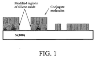
- the validity of the proposed method is demonstrated with molecules of ⁇ -sexithionyl (T6) deposited by sublimation in an ultra high vacuum chamber. Due to the kinetics of the growth and the preferential, though non-specific, interactions of the molecules with the silicon oxide regions, structures of organic molecules are formed which reproduce the shape and size of the nanostructures (see Figure 1 and Figures 3 and 4).
- the tracks or strips of organic molecules have a length of several microns and their width varies between 100 and 600 nm. From the height of the molecules, it is deduced that they are orientated with their longitudinal axis perpendicular to the substrate.
- the same material grown on an unmodified silicon substrate does not give rise to the formation of ordered structures.
- the molecules are grouped forming islands of irregular shape and distribution and with diameters of several microns.
- the proposed method could be used for manufacturing wires and conduction channels in integrated circuits made of a plastic material with pattern densities of between three and ten times greater than those obtained with ultraviolet optical lithography.
- the silicon oxide regions were obtained by means of anodic oxidation, for which purpose an atomic-force microscope (AFM) was used.
- the method is known as local oxidation nanolithography A detailed description of it can be found in references 1-4. Nevertheless, the process is completely general and valid for any production method of anodic silicon oxides.
- an integrated circuit could be manufactured with active elements formed by organic molecules and with a pattern density of between three and ten times greater than those obtained with ultraviolet optical lithography.
- the silicon oxide regions were obtained by means of anodic oxidation, for which purpose an atomic-force microscope (AFM) was used.
- the method is known as local oxidation nanolithography A detailed description of it can be found in references 1-4. Nevertheless, the process is completely general and independent of the technique employed for producing anodic oxides.
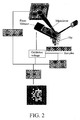
- the arrangement used for carrying out anodic oxidation is shown in diagrammatic form in figure 2.
- the head of an atomic-force microscope is introduced into a chamber permitting control of the relative humidity.
- the relative humidity is kept at between 30-50%.
- the oxidations are carried out with silicon microlevers (n+) characterised by force constants of between 30-40 N/m and resonance frequencies between 300-400 kHz.
- the semiconductor samples were of Si(100) type p and with resistivities of 14 ⁇ cm.
- the local oxidation process in the mode of atomic-force microscope non-contact requires several stages.
- the tip-microlever system oscillates at a distance of about 5 nm from the sample surface.
- the surface of the sample has previously been coated with a few monolayers of water.
- a voltage is applied between the tip and sample. If the applied voltage exceeds a certain threshold value, a neck of water of formed between the two surfaces.
- Another voltage pulse is then introduced in order to initiate the oxidation.
- the microscope returns to the visualisation mode, which permits images of the modified zones to be taken. In certain situations, those which have been used in these experiments, the same voltage pulse can be used to form the neck and grow the oxide.
- the electron current measured during the oxidation process is very close to that expected for anodic oxidation processes if it is calculated starting from the volume of oxide generated and it is assumed that the reaction is described by Si + 2h + + 2 (OH) ⁇ SiO 2 + H 2 (1)
- the above reaction implies the decomposition of water molecules according to 2H 2 ⁇ 2H + + 2(OH - (2) while the oxidation that takes place in the anode (here the sample) is described as Si + 2h+ + 2(OH - ⁇ Si(OH) 2 ⁇ SiO 2 + 2H+ +2e- (3)
- the process involves the generation at the cathode according to 2H+ + 2e- ⁇ H2 (4) Nevertheless, the proximity existing between the tip and the sample and the application of voltage pulses in the range 10-20 V originates high electric fields (E ⁇ 1-3 V/nm). Those fields modify the chemical equilibrium established by the above equations and favours the distribution of defects in the oxide. As a consequence, a high concentration
- a series of parallel tracks have been manufactured of length 6 ⁇ m, width 360-550 nm and height 3 nm (Figure 4).
- the height of the patterns almost coincides with the Van de Waals length of T6 (2.7 nm).
- Each track is composed of eight lines and each line is a sequence of oxide points.
- the separation between oxide points (- 10 nm) is less than their diameter (- 20-40 nm); as a consequence, the points overlap and a continuous line is formed.
- the oxide points have been obtained by means of the application of a voltage peak of 20 V during 10 ms.
- the sample with the oxide patterns had been manufactured, it was transferred to the ultra high vacuum chamber in order to proceed with deposition of the molecules.
- the results obtained by Biscarini et al. were applied, which demonstrate a layer to layer growth in a band of deposition temperatures (50-150° 1C) and small thicknesses (1-10 microns) [6-9].
- rated thicknesses of 1.5 nm were deposited while the sample was kept at a temperature of 150 °C.
- Figures 5(a) and (b) show the results obtained. We wish to emphasise three results. First, away from the modified zones the molecules display morphologies characterised by islands having a fractal appearance and characteristic dimensions of 1 ⁇ m. Second, within the modified zone the molecules preferentially grow along the oxide tracks. The coating of the molecules is greater on the tracks than on the unmodified zones between them. Third, the continuity of the film depends on the lateral spacing of the oxide lines forming the tracks. Those tracks whose lines are more separated show more fractures in the organic film. In the first track from the left ( Figure 5), the lines forming the track overlap giving rise to a uniform and continuous film. In some zones of the film the molecules also display a lateral growth with dendritic shapes. This growth indicates that there exists an excess of molecules since not all of them can be accommodated on the oxide track.
- the lateral separation of the lines is increased, the continuity of the film is broken.
- the above images permit the inference that the growth of a continuous film in an arbitrary manner is a competition between the diffusion coefficient of the molecules on the unmodified substrate, the density of the molecules and the preferential growth observed on the oxide lines.
- the preferential growth along the oxide lines increases when the number of oxidations effected in order to form the line is increased.
- the density of defects is controlled by reducing the lateral separation of the individual lines.
- Figure 6 shows tracks or strips of organic molecules grown by means of the proposed method.
- the pattern that is manufactured has the shape of an orthodox cross with tracks that cut each other perpendicularly (Fig. 6a).
- the difference between the density and uniformity of the domains of molecules on the oxide nanostructures and on the unmodified substrate does not cease to cause surprise.
Landscapes
- Formation Of Insulating Films (AREA)
Abstract
The invention relates to a method of controlling the spatial distribution, shape and size of films of conjugated organic molecules. The inventive method can be used to grow single layers of organic molecules on silicon oxide nanostructures. The silicon oxide nanostructures are produced using an anodic oxidation process. The organisation of the molecules on the oxide nanostructures is dependent on the kinetic parameters of the latter (evaporation rate, diffusion coefficient) and on the interactions with the silicon (anodic) oxide regions. The molecules form domains which exactly reproduce the lateral size and the shape of the oxide nanostructures. The invention provides a powerful method of performing a bottom-up construction of wires, electrodes and charge transfer zones in nanoscale devices.
Description
- Nanoscale manufacturing processes for polymer structures and thin films of organic molecules.
- Conjugated materials constitute a family of organic materials formed from coordinated compounds, polymers, copolymers and polymer mixtures which are characterised by the existence of functional groups with electron orbitals delocalised on different carbon atoms or other atoms, fundamentally nitrogen, oxygen or sulphur. These materials display optical and electronic properties similar to those observed in silicon or III-V semiconductors and are generically referred to as organic semiconductors. The spatial distribution of the charge density of the pi orbitals is highly anisotropic and as a consequence their optical and electronic properties depend on the orientation and on the molecular groupings.
- Plastic electronics is a new sustainable type technology based on the use of thin films of conjugated compounds whose thicknesses vary between 1 and 100 nm. The products of plastic electronics are complementary to those of microelectronics since they are concentrated in low cost applications and they can take recycling or their waste has a very low environmental impact. As examples, mention can be made of the manufacture of labels, cards and intelligent clothing or electronic Identity cards. Conjugated compounds are easy to process and compatible with microelectronic processes. Nevertheless, it is crucial to control the molecular orientation, the order and the anisotropy of the molecular domains in order to obtain efficient devices.
- The improvement in the electronic properties of a device formed from electronic molecules requires an understanding and control of the interactions between the organic molecules and the biological material. This is a complex problem since in an integrated circuit type device there co-exist regions of differing properties, both chemical and electrical or topographical. All this means that the molecules undergo different interactions. This heterogeneity has an influence on the nucleation and growth processes, which in the end will determine the structure and morphology of the film. A self-organised growth would be very desirable since it would permit the active elements to be connected to the electrodes which would lead to a growth in the integration of the devices. All this makes it necessary to develop new procedures for promoting the spontaneous organisation of organic molecules.
- Cited below are some patents for obtaining nanostructures of organic materials.
- 1. Kano et al., Alps Electric Co. Ltd. (JP) Appl. No. 170715 October 13, 1998;
- 2. Cox et al., Borealis Technical Limited (London UK), Appl. No. 045299 March 20, 1998;
- 3. Biebuyck and Michel, International Business Machine Corporation (Armonk NY), Appl. No. 690956 August 1, 1996;
- 4. Calveley (Private Bag, MBE N180 Auckland, NZ) Appl. No. 474420, December 29, 1999;
- 5. Chou S. and Zhuang L. (Princeton University NJ), Appl. No. US23717 October 8, 1999.
- 6. M. Murgia, P. Mei, F. Biscarini, C. Taliani (CNR-ISM Bologna, Italy) Italian Appl. No. MI 2000 A002075 October 8 2001, extension PCT/EP02/11218 on October 7.
- 7. Katz H. E. (Agere Systems Guardian Corp. Orlando, FL), Appl. No. US605507 June 28, 2000.
- 8. Bulovic V. and Forrest S. R. (The Trustees of Princeton University, Princeton NJ) Appl. No. US 717351, November 22, 2000.
- 9. Cavallini M. and Biscarini F. (CNR-ISMN Sez. Bologna, Italy) Italian Appl. MI2002A001961, September 16, 2002.
- A sign of the impact of nanotechnology on the economic growth of developed economies can be seen from the level of government investment in Europe, USA and Japan. For example, in the sixth framework programme of the EU, nanotechnology is a priority area with financing of more than 1300 M€.
- The invention consists of a process which permits the growth of organic molecules in defined regions of a silicon substrate. The said regions are defined by means of the anodic oxidation of a selective region of the sample. The anodic oxidation process produces a silicon oxide with numerous defects which modifies both the topography and the chemical composition. The oxidation is used to create structures extending from a few nanometres up to tens of microns. The shape and periodicity of the nanostructures is variable. Matrices of points, lines, matrices of parallel lines, tracks and circles have been manufactured.
- The molecules preferentially nucleate on the oxide nanostructures, which originates a monolayer of molecules that reproduce the shape and size of the silicon oxide nanostructure. The validity of the proposed method is demonstrated with molecules of α-sexithionyl (T6) deposited by sublimation in an ultra high vacuum chamber. Due to the kinetics of the growth and the preferential, though non-specific, interactions of the molecules with the silicon oxide regions, structures of organic molecules are formed which reproduce the shape and size of the nanostructures (see Figure 1 and Figures 3 and 4). The tracks or strips of organic molecules have a length of several microns and their width varies between 100 and 600 nm. From the height of the molecules, it is deduced that they are orientated with their longitudinal axis perpendicular to the substrate.
- The same material grown on an unmodified silicon substrate does not give rise to the formation of ordered structures. The molecules are grouped forming islands of irregular shape and distribution and with diameters of several microns.
- The proposed method could be used for manufacturing wires and conduction channels in integrated circuits made of a plastic material with pattern densities of between three and ten times greater than those obtained with ultraviolet optical lithography.
- The silicon oxide regions were obtained by means of anodic oxidation, for which purpose an atomic-force microscope (AFM) was used. The method is known as local oxidation nanolithography A detailed description of it can be found in references 1-4. Nevertheless, the process is completely general and valid for any production method of anodic silicon oxides.
- With the proposed method, an integrated circuit could be manufactured with active elements formed by organic molecules and with a pattern density of between three and ten times greater than those obtained with ultraviolet optical lithography.
- The silicon oxide regions were obtained by means of anodic oxidation, for which purpose an atomic-force microscope (AFM) was used. The method is known as local oxidation nanolithography A detailed description of it can be found in references 1-4. Nevertheless, the process is completely general and independent of the technique employed for producing anodic oxides.
- The arrangement used for carrying out anodic oxidation is shown in diagrammatic form in figure 2. The head of an atomic-force microscope is introduced into a chamber permitting control of the relative humidity. The relative humidity is kept at between 30-50%. The oxidations are carried out with silicon microlevers (n+) characterised by force constants of between 30-40 N/m and resonance frequencies between 300-400 kHz. The semiconductor samples were of Si(100) type p and with resistivities of 14 Ω cm.
- The local oxidation process in the mode of atomic-force microscope non-contact requires several stages. First, the tip-microlever system oscillates at a distance of about 5 nm from the sample surface. The surface of the sample has previously been coated with a few monolayers of water. After that, a voltage is applied between the tip and sample. If the applied voltage exceeds a certain threshold value, a neck of water of formed between the two surfaces. Another voltage pulse is then introduced in order to initiate the oxidation. Once the above process has been completed, the microscope returns to the visualisation mode, which permits images of the modified zones to be taken. In certain situations, those which have been used in these experiments, the same voltage pulse can be used to form the neck and grow the oxide.
- The electron current measured during the oxidation process is very close to that expected for anodic oxidation processes if it is calculated starting from the volume of oxide generated and it is assumed that the reaction is described by
Si + 2h+ + 2 (OH) ⇒SiO2 + H2 (1)
The above reaction implies the decomposition of water molecules according to
2H2⇒2H+ + 2(OH- (2)
while the oxidation that takes place in the anode (here the sample) is described as
Si + 2h+ + 2(OH-⇒Si(OH)2⇒SiO2 + 2H+ +2e- (3)
Furthermore, the process involves the generation at the cathode according to
2H+ + 2e- ⇒H2 (4)
Nevertheless, the proximity existing between the tip and the sample and the application of voltage pulses in the range 10-20 V originates high electric fields (E ~ 1-3 V/nm). Those fields modify the chemical equilibrium established by the above equations and favours the distribution of defects in the oxide. As a consequence, a high concentration of positively charged defects H30+--O-si are generated in the proximity of the Si/SiOx interface. - In order to demonstrate the advantages of the proposed method for controlling and directing the growth of molecular films at the nanoscale, a series of parallel tracks have been manufactured of length 6 µm, width 360-550 nm and height 3 nm (Figure 4). The height of the patterns almost coincides with the Van de Waals length of T6 (2.7 nm). Each track is composed of eight lines and each line is a sequence of oxide points. The separation between oxide points (- 10 nm) is less than their diameter (- 20-40 nm); as a consequence, the points overlap and a continuous line is formed. The oxide points have been obtained by means of the application of a voltage peak of 20 V during 10 ms.
- Once the sample with the oxide patterns had been manufactured, it was transferred to the ultra high vacuum chamber in order to proceed with deposition of the molecules. During the deposition, the results obtained by Biscarini et al. were applied, which demonstrate a layer to layer growth in a band of deposition temperatures (50-150° 1C) and small thicknesses (1-10 microns) [6-9]. In these experiments, rated thicknesses of 1.5 nm were deposited while the sample was kept at a temperature of 150 °C.
- Figures 5(a) and (b) show the results obtained. We wish to emphasise three results. First, away from the modified zones the molecules display morphologies characterised by islands having a fractal appearance and characteristic dimensions of 1 µm. Second, within the modified zone the molecules preferentially grow along the oxide tracks. The coating of the molecules is greater on the tracks than on the unmodified zones between them. Third, the continuity of the film depends on the lateral spacing of the oxide lines forming the tracks. Those tracks whose lines are more separated show more fractures in the organic film. In the first track from the left (Figure 5), the lines forming the track overlap giving rise to a uniform and continuous film. In some zones of the film the molecules also display a lateral growth with dendritic shapes. This growth indicates that there exists an excess of molecules since not all of them can be accommodated on the oxide track.
- Moreover, when the lateral separation of the lines is increased, the continuity of the film is broken. The above images permit the inference that the growth of a continuous film in an arbitrary manner is a competition between the diffusion coefficient of the molecules on the unmodified substrate, the density of the molecules and the preferential growth observed on the oxide lines. The preferential growth along the oxide lines increases when the number of oxidations effected in order to form the line is increased. Here, the density of defects is controlled by reducing the lateral separation of the individual lines.
- Figure 6 shows tracks or strips of organic molecules grown by means of the proposed method. The pattern that is manufactured has the shape of an orthodox cross with tracks that cut each other perpendicularly (Fig. 6a). The difference between the density and uniformity of the domains of molecules on the oxide nanostructures and on the unmodified substrate does not cease to cause surprise.
- To summarise, the present development demonstrates that control of the kinetic parameters during growth and the existence of preferential interactions of organic molecules with the silicon oxide structures make it possible to carry out the nanoscale manufacture of structures formed by conjugated molecules.
-
- Figure 1. Diagram of the result of the invention. The organic molecules spontaneously grow on the manufactured zones of silicon oxide. The size and shape of the molecular film is controlled by the nanostructure of the oxide. outside the modified regions the molecules adopt irregular shapes and sizes.
- Figure 2. Diagram of the arrangement used for carrying out the anodic oxidation.
- Figure 3. Diagram of the local oxidation process used in this patent.
- Figure 4. AFM image of a series of parallel tracks manufactured by the method of anodic oxidation of silicon.
- Figure 5. (a) AFM image of silicon oxide nanostructures after the deposition of 1.5 nm of T6 molecules. (b) Section of the previous image. The continuity of the organic film is obtained by increasing the density of anodic oxide patterns.
- Figure 6. (a) AFM image of orthogonal tracks of silicon oxide. (b) AFM image after deposition of molecules on the structure shown in (a).
-
- 1. R. Garcia, M. Calleja, F. Pérez-Murano, Appl. Phys. Lett. 72, 2295 (1998).
- 2. R. Garcia, M. Calleja and H. Rohrer, J. Appl. Phys. 86, 1898 (1999).
- 3. M. Calleja and R. Garcia, Appl. Phys. Lett. 76, 3427 (2000).
- 4. M. Tello and R. Garcia, Appl. Phys. Lett. 79, 424 (2001).
- 5. J. A. Dagata, T. Inoue, J. Itoh, K. Matsumoto, H. Yokoyama, J. Appl. Phys., 84, 6891 (1998).
- 6. F. Biscarini, R. Zamboni, P. Samorí, P. Ostoja and C. Taliani, "Growth of Conjugated Oligomer Thin Films Studied by Atomic-Force Microscopy", Phys. Rev. B 52, 14868 (1995).
- 7. S. Prato, L. Floreano, D. Cvetko, V. DeRenzi, A, Morgante, S. Modesti, F. Biscarini, C. Taliani, R. Zamboni, "Anisotropic Ordered Planar Growth of a-sexithienyl Thin Films", J. Phys. Chem. B 37, 7788 (1999).
- 8. M. Brinkmann, F. Biscarini, C. Taliani, I. Aiello and M. Ghedini, "Growth of Mesoscopic Correlated Droplet Patterns by High-Vacuum Sublimation", Phys. Rev. B Rapid Comm. 61, R16339 (2000).
Claims (9)
- A method for controlling the growth of organic films formed by conjugated molecules in predefined sites of a silicon substrate. The method is based on the preferential but non-specific interactions of the molecules with regions of anodic silicon oxide that have been generated by lithographic methods.
- According to claim 1, a method based on the use of anodic oxides for promoting nucleation and growth of the molecules on the oxide nanostructures.
- Process for controlling the growth of conjugated organic molecules on predefined regions of a silicon substrate (with or without the presence of an oxide layer, whether this be thermal or native). Those regions have been manufactured by anodic oxidation by means of an atomic-force microscope.
- Process for controlling the growth of molecules of α-sexithienyl on predefined regions of a silicon substrate (with or without the presence of an oxide layer, whether this be thermal or native). Those regions have been manufactured by anodic oxidation by means of an atomic-force microscope.
- Process for controlling the growth of molecules of α-sexithienyl on structures manufactured by means of anodic oxidation of silicon.
- Method according to claims 1 and 2 for improving the properties of the monolayers by increasing the density of oxide patterns.
- According to claims 1 and 3, a method is proposed for optimising the organisation of molecular domains of variable shape and size between a few nanometres and several microns.
- According to claim 4, a process is proposed for forming wires, tracks and molecular regions of α-sexithienyl.
- From claims 1 and 4 a process is proposed for introducing length scales extrinsic to the molecules employed.
Applications Claiming Priority (2)
| Application Number | Priority Date | Filing Date | Title |
|---|---|---|---|
| ES200300565A ES2229883B1 (en) | 2003-03-07 | 2003-03-07 | PROCEDURE FOR MANUFACTURING FILMS OF CONJUGATED ORGANIC MOLECULES AND THEIR APPLICATIONS. |
| PCT/ES2004/070013 WO2004079835A1 (en) | 2003-03-07 | 2004-03-08 | Nanoscale control of the spatial distribution, shape and size of thin films of conjugated organic molecules through the production of silicon oxide nanostructures |
Publications (1)
| Publication Number | Publication Date |
|---|---|
| EP1617492A1 true EP1617492A1 (en) | 2006-01-18 |
Family
ID=32947015
Family Applications (1)
| Application Number | Title | Priority Date | Filing Date |
|---|---|---|---|
| EP04718319A Withdrawn EP1617492A1 (en) | 2003-03-07 | 2004-03-08 | Nanoscale control of the spatial distribution, shape and size of thin films of conjugated organic molecules through the production of silicon oxide nanostructures |
Country Status (4)
| Country | Link |
|---|---|
| US (1) | US7498060B2 (en) |
| EP (1) | EP1617492A1 (en) |
| ES (1) | ES2229883B1 (en) |
| WO (1) | WO2004079835A1 (en) |
Families Citing this family (1)
| Publication number | Priority date | Publication date | Assignee | Title |
|---|---|---|---|---|
| EP2045818B1 (en) * | 2006-07-04 | 2019-05-08 | Consejo Superior de Investigaciones Cientificas (CSIC) | Method for using an atomic force microscope |
Family Cites Families (10)
| Publication number | Priority date | Publication date | Assignee | Title |
|---|---|---|---|---|
| US3663870A (en) * | 1968-11-13 | 1972-05-16 | Tokyo Shibaura Electric Co | Semiconductor device passivated with rare earth oxide layer |
| US4674320A (en) * | 1985-09-30 | 1987-06-23 | The United States Of America As Represented By The United States Department Of Energy | Chemoresistive gas sensor |
| US6326640B1 (en) * | 1996-01-29 | 2001-12-04 | Motorola, Inc. | Organic thin film transistor with enhanced carrier mobility |
| US6117344A (en) * | 1998-03-20 | 2000-09-12 | Borealis Technical Limited | Method for manufacturing low work function surfaces |
| US6127004A (en) * | 1999-01-29 | 2000-10-03 | Eastman Kodak Company | Forming an amorphous fluorocarbon layer in electroluminescent devices |
| US6887332B1 (en) * | 2000-04-21 | 2005-05-03 | International Business Machines Corporation | Patterning solution deposited thin films with self-assembled monolayers |
| US6403397B1 (en) * | 2000-06-28 | 2002-06-11 | Agere Systems Guardian Corp. | Process for fabricating organic semiconductor device involving selective patterning |
| US7098145B2 (en) * | 2000-12-04 | 2006-08-29 | Seiko Epson Corporation | Fabrication of self-assembled monolayers |
| CA2457791C (en) * | 2001-08-20 | 2010-08-03 | Nova-Plasma Inc. | Coatings with low permeation of gases and vapors |
| US7166327B2 (en) * | 2003-03-21 | 2007-01-23 | International Business Machines Corporation | Method of preparing a conjugated molecular assembly |
-
2003
- 2003-03-07 ES ES200300565A patent/ES2229883B1/en not_active Expired - Fee Related
-
2004
- 2004-03-08 EP EP04718319A patent/EP1617492A1/en not_active Withdrawn
- 2004-03-08 WO PCT/ES2004/070013 patent/WO2004079835A1/en not_active Ceased
-
2005
- 2005-09-07 US US11/220,896 patent/US7498060B2/en not_active Expired - Fee Related
Non-Patent Citations (1)
| Title |
|---|
| See references of WO2004079835A1 * |
Also Published As
| Publication number | Publication date |
|---|---|
| US20070234947A1 (en) | 2007-10-11 |
| ES2229883B1 (en) | 2006-07-01 |
| US7498060B2 (en) | 2009-03-03 |
| ES2229883A1 (en) | 2005-04-16 |
| WO2004079835A1 (en) | 2004-09-16 |
| WO2004079835B1 (en) | 2004-10-21 |
Similar Documents
| Publication | Publication Date | Title |
|---|---|---|
| Chang et al. | Densely packed arrays of ultra‐high‐aspect‐ratio silicon nanowires fabricated using block‐copolymer lithography and metal‐assisted etching | |
| US8802047B2 (en) | Embedded nanoparticle films and method for their formation in selective areas on a surface | |
| US20130160701A1 (en) | Barrier guided growth of microstructured and nanostructured graphene and graphite | |
| Wu et al. | Fabrication of a class of nanostructured materials using carbon nanowalls as the templates | |
| US8377323B2 (en) | Mold having nanometric features, method for realizing such a mold and corresponding use of it in a method for realizing an array of carbon nanotubes | |
| Dong et al. | Theoretical study of chemical vapor deposition synthesis of graphene and beyond: challenges and perspectives | |
| US9213241B2 (en) | Method of making nanostructure | |
| GB2387272A (en) | Nanopore structure for aligning molecules for molecular electronics | |
| CN100577290C (en) | Preparation of catalyst layer for synthesizing carbon nanotubes and method for synthesizing carbon nanotubes therewith | |
| JP4234348B2 (en) | Inter-pattern wiring formation method | |
| KR100973522B1 (en) | Method of manufacturing ruthenium nanostructures using anodized aluminum oxide and atomic layer deposition process | |
| WO2021133840A1 (en) | Block copolymer self-alignment on isolated chemical stripes | |
| US7498060B2 (en) | Method for controlling at nanometric scale the growth of thin films of conjugated organic molecules | |
| KR20090114653A (en) | Method for preparing nanostructures using liquid vapor deposition technique and nanostructures produced by the same | |
| KR101356010B1 (en) | Method for manufacturing nanostructure using 2-dimensional transfer layer, nanostructure manufactured by the same and application device comprising the same | |
| JP2001007315A (en) | Method of forming quantum dots | |
| Ghoshal et al. | Development of a facile block copolymer method for creating hard mask patterns integrated into semiconductor manufacturing | |
| Ding et al. | Fabrication of highly ordered nanocrystalline Si: H nanodots for the application of nanodevice arrays | |
| Biscarini et al. | Nanoscale control ofthe spatial distribution, shape and size ofthin films of conjugated organic molecules through the production of sillcon oxide nanostructures. | |
| Ferri et al. | Ultradense silicon nanowire arrays produced via top-down planar technology | |
| Ding et al. | Fabrication of nanocrystalline Si: H nanodot arrays with controllable porous alumina membranes | |
| Lee et al. | Patterning of various silicon structures via polymer lithography and catalytic chemical etching | |
| Su et al. | Boundary-Directed Epitaxy of Block Copolymers Toward Sub-10 nm Fabrication | |
| Lee | Nanoscale Engineering for Mixed-Dimensional Heterostructure Growth and Integration | |
| Kuo et al. | Novel selective process via self-assembled monolayers for pattern growth of carbon nanotubes |
Legal Events
| Date | Code | Title | Description |
|---|---|---|---|
| PUAI | Public reference made under article 153(3) epc to a published international application that has entered the european phase |
Free format text: ORIGINAL CODE: 0009012 |
|
| 17P | Request for examination filed |
Effective date: 20051006 |
|
| AK | Designated contracting states |
Kind code of ref document: A1 Designated state(s): AT BE BG CH CY CZ DE DK EE ES FI FR GB GR HU IE IT LI LU MC NL PL PT RO SE SI SK TR |
|
| AX | Request for extension of the european patent |
Extension state: AL LT LV MK |
|
| DAX | Request for extension of the european patent (deleted) | ||
| 17Q | First examination report despatched |
Effective date: 20110802 |
|
| STAA | Information on the status of an ep patent application or granted ep patent |
Free format text: STATUS: THE APPLICATION IS DEEMED TO BE WITHDRAWN |
|
| 18D | Application deemed to be withdrawn |
Effective date: 20111001 |