EP1617244A1 - Optical device including a Bragg grating and method of manufacturing thereof - Google Patents
Optical device including a Bragg grating and method of manufacturing thereof Download PDFInfo
- Publication number
- EP1617244A1 EP1617244A1 EP04103032A EP04103032A EP1617244A1 EP 1617244 A1 EP1617244 A1 EP 1617244A1 EP 04103032 A EP04103032 A EP 04103032A EP 04103032 A EP04103032 A EP 04103032A EP 1617244 A1 EP1617244 A1 EP 1617244A1
- Authority
- EP
- European Patent Office
- Prior art keywords
- waveguide
- bragg grating
- optical
- support substrate
- substrate
- Prior art date
- Legal status (The legal status is an assumption and is not a legal conclusion. Google has not performed a legal analysis and makes no representation as to the accuracy of the status listed.)
- Withdrawn
Links
- 230000003287 optical effect Effects 0.000 title claims abstract description 125
- 238000004519 manufacturing process Methods 0.000 title description 14
- 239000000758 substrate Substances 0.000 claims abstract description 100
- 238000000034 method Methods 0.000 claims abstract description 27
- 230000008878 coupling Effects 0.000 claims abstract description 8
- 238000010168 coupling process Methods 0.000 claims abstract description 8
- 238000005859 coupling reaction Methods 0.000 claims abstract description 8
- 239000000463 material Substances 0.000 claims description 24
- 230000004044 response Effects 0.000 claims description 13
- 230000008859 change Effects 0.000 claims description 2
- 238000005476 soldering Methods 0.000 claims 1
- 239000003017 thermal stabilizer Substances 0.000 claims 1
- 239000000835 fiber Substances 0.000 description 71
- 238000004891 communication Methods 0.000 description 11
- 239000013307 optical fiber Substances 0.000 description 9
- 238000004806 packaging method and process Methods 0.000 description 9
- 230000033228 biological regulation Effects 0.000 description 6
- 239000004065 semiconductor Substances 0.000 description 6
- 229910000679 solder Inorganic materials 0.000 description 5
- 239000004020 conductor Substances 0.000 description 4
- 239000002184 metal Substances 0.000 description 4
- 229910052751 metal Inorganic materials 0.000 description 4
- 238000001228 spectrum Methods 0.000 description 4
- 229910001218 Gallium arsenide Inorganic materials 0.000 description 3
- 230000008602 contraction Effects 0.000 description 3
- 238000000295 emission spectrum Methods 0.000 description 3
- 238000001465 metallisation Methods 0.000 description 3
- 230000005855 radiation Effects 0.000 description 3
- 230000001105 regulatory effect Effects 0.000 description 3
- 229910052710 silicon Inorganic materials 0.000 description 3
- 239000010703 silicon Substances 0.000 description 3
- 230000005540 biological transmission Effects 0.000 description 2
- 150000002739 metals Chemical class 0.000 description 2
- 230000000087 stabilizing effect Effects 0.000 description 2
- 229910000881 Cu alloy Inorganic materials 0.000 description 1
- 229910000577 Silicon-germanium Inorganic materials 0.000 description 1
- 229910045601 alloy Inorganic materials 0.000 description 1
- 239000000956 alloy Substances 0.000 description 1
- 230000001276 controlling effect Effects 0.000 description 1
- 238000013461 design Methods 0.000 description 1
- 238000010586 diagram Methods 0.000 description 1
- 229910003460 diamond Inorganic materials 0.000 description 1
- 239000010432 diamond Substances 0.000 description 1
- 230000000694 effects Effects 0.000 description 1
- 230000005684 electric field Effects 0.000 description 1
- 230000002708 enhancing effect Effects 0.000 description 1
- 230000001747 exhibiting effect Effects 0.000 description 1
- 230000017525 heat dissipation Effects 0.000 description 1
- 229910000833 kovar Inorganic materials 0.000 description 1
- 239000007769 metal material Substances 0.000 description 1
- 238000012986 modification Methods 0.000 description 1
- 230000004048 modification Effects 0.000 description 1
- 229910003465 moissanite Inorganic materials 0.000 description 1
- 238000012544 monitoring process Methods 0.000 description 1
- 238000002310 reflectometry Methods 0.000 description 1
- 229910010271 silicon carbide Inorganic materials 0.000 description 1
- 230000003595 spectral effect Effects 0.000 description 1
- 238000002211 ultraviolet spectrum Methods 0.000 description 1
- 238000001429 visible spectrum Methods 0.000 description 1
Images


Classifications
-
- H—ELECTRICITY
- H01—ELECTRIC ELEMENTS
- H01S—DEVICES USING THE PROCESS OF LIGHT AMPLIFICATION BY STIMULATED EMISSION OF RADIATION [LASER] TO AMPLIFY OR GENERATE LIGHT; DEVICES USING STIMULATED EMISSION OF ELECTROMAGNETIC RADIATION IN WAVE RANGES OTHER THAN OPTICAL
- H01S5/00—Semiconductor lasers
- H01S5/02—Structural details or components not essential to laser action
- H01S5/022—Mountings; Housings
- H01S5/023—Mount members, e.g. sub-mount members
- H01S5/02325—Mechanically integrated components on mount members or optical micro-benches
-
- G—PHYSICS
- G02—OPTICS
- G02B—OPTICAL ELEMENTS, SYSTEMS OR APPARATUS
- G02B6/00—Light guides; Structural details of arrangements comprising light guides and other optical elements, e.g. couplings
- G02B6/02—Optical fibres with cladding with or without a coating
- G02B6/02057—Optical fibres with cladding with or without a coating comprising gratings
- G02B6/02076—Refractive index modulation gratings, e.g. Bragg gratings
- G02B6/02171—Refractive index modulation gratings, e.g. Bragg gratings characterised by means for compensating environmentally induced changes
- G02B6/02176—Refractive index modulation gratings, e.g. Bragg gratings characterised by means for compensating environmentally induced changes due to temperature fluctuations
-
- G—PHYSICS
- G02—OPTICS
- G02B—OPTICAL ELEMENTS, SYSTEMS OR APPARATUS
- G02B6/00—Light guides; Structural details of arrangements comprising light guides and other optical elements, e.g. couplings
- G02B6/02—Optical fibres with cladding with or without a coating
- G02B6/02057—Optical fibres with cladding with or without a coating comprising gratings
- G02B6/02076—Refractive index modulation gratings, e.g. Bragg gratings
- G02B6/02195—Refractive index modulation gratings, e.g. Bragg gratings characterised by means for tuning the grating
- G02B6/022—Refractive index modulation gratings, e.g. Bragg gratings characterised by means for tuning the grating using mechanical stress, e.g. tuning by compression or elongation, special geometrical shapes such as "dog-bone" or taper
-
- G—PHYSICS
- G02—OPTICS
- G02B—OPTICAL ELEMENTS, SYSTEMS OR APPARATUS
- G02B6/00—Light guides; Structural details of arrangements comprising light guides and other optical elements, e.g. couplings
- G02B6/24—Coupling light guides
- G02B6/42—Coupling light guides with opto-electronic elements
- G02B6/4201—Packages, e.g. shape, construction, internal or external details
- G02B6/4204—Packages, e.g. shape, construction, internal or external details the coupling comprising intermediate optical elements, e.g. lenses, holograms
- G02B6/421—Packages, e.g. shape, construction, internal or external details the coupling comprising intermediate optical elements, e.g. lenses, holograms the intermediate optical component consisting of a short length of fibre, e.g. fibre stub
-
- H—ELECTRICITY
- H01—ELECTRIC ELEMENTS
- H01S—DEVICES USING THE PROCESS OF LIGHT AMPLIFICATION BY STIMULATED EMISSION OF RADIATION [LASER] TO AMPLIFY OR GENERATE LIGHT; DEVICES USING STIMULATED EMISSION OF ELECTROMAGNETIC RADIATION IN WAVE RANGES OTHER THAN OPTICAL
- H01S5/00—Semiconductor lasers
- H01S5/10—Construction or shape of the optical resonator, e.g. extended or external cavity, coupled cavities, bent-guide, varying width, thickness or composition of the active region
- H01S5/14—External cavity lasers
- H01S5/146—External cavity lasers using a fiber as external cavity
-
- H—ELECTRICITY
- H01—ELECTRIC ELEMENTS
- H01S—DEVICES USING THE PROCESS OF LIGHT AMPLIFICATION BY STIMULATED EMISSION OF RADIATION [LASER] TO AMPLIFY OR GENERATE LIGHT; DEVICES USING STIMULATED EMISSION OF ELECTROMAGNETIC RADIATION IN WAVE RANGES OTHER THAN OPTICAL
- H01S3/00—Lasers, i.e. devices using stimulated emission of electromagnetic radiation in the infrared, visible or ultraviolet wave range
- H01S3/10—Controlling the intensity, frequency, phase, polarisation or direction of the emitted radiation, e.g. switching, gating, modulating or demodulating
- H01S3/105—Controlling the intensity, frequency, phase, polarisation or direction of the emitted radiation, e.g. switching, gating, modulating or demodulating by controlling the mutual position or the reflecting properties of the reflectors of the cavity, e.g. by controlling the cavity length
- H01S3/1053—Control by pressure or deformation
-
- H—ELECTRICITY
- H01—ELECTRIC ELEMENTS
- H01S—DEVICES USING THE PROCESS OF LIGHT AMPLIFICATION BY STIMULATED EMISSION OF RADIATION [LASER] TO AMPLIFY OR GENERATE LIGHT; DEVICES USING STIMULATED EMISSION OF ELECTROMAGNETIC RADIATION IN WAVE RANGES OTHER THAN OPTICAL
- H01S5/00—Semiconductor lasers
- H01S5/02—Structural details or components not essential to laser action
- H01S5/022—Mountings; Housings
- H01S5/02208—Mountings; Housings characterised by the shape of the housings
- H01S5/02216—Butterfly-type, i.e. with electrode pins extending horizontally from the housings
-
- H—ELECTRICITY
- H01—ELECTRIC ELEMENTS
- H01S—DEVICES USING THE PROCESS OF LIGHT AMPLIFICATION BY STIMULATED EMISSION OF RADIATION [LASER] TO AMPLIFY OR GENERATE LIGHT; DEVICES USING STIMULATED EMISSION OF ELECTROMAGNETIC RADIATION IN WAVE RANGES OTHER THAN OPTICAL
- H01S5/00—Semiconductor lasers
- H01S5/02—Structural details or components not essential to laser action
- H01S5/022—Mountings; Housings
- H01S5/0225—Out-coupling of light
- H01S5/02251—Out-coupling of light using optical fibres
-
- H—ELECTRICITY
- H01—ELECTRIC ELEMENTS
- H01S—DEVICES USING THE PROCESS OF LIGHT AMPLIFICATION BY STIMULATED EMISSION OF RADIATION [LASER] TO AMPLIFY OR GENERATE LIGHT; DEVICES USING STIMULATED EMISSION OF ELECTROMAGNETIC RADIATION IN WAVE RANGES OTHER THAN OPTICAL
- H01S5/00—Semiconductor lasers
- H01S5/02—Structural details or components not essential to laser action
- H01S5/024—Arrangements for thermal management
- H01S5/02407—Active cooling, e.g. the laser temperature is controlled by a thermo-electric cooler or water cooling
- H01S5/02415—Active cooling, e.g. the laser temperature is controlled by a thermo-electric cooler or water cooling by using a thermo-electric cooler [TEC], e.g. Peltier element
-
- H—ELECTRICITY
- H01—ELECTRIC ELEMENTS
- H01S—DEVICES USING THE PROCESS OF LIGHT AMPLIFICATION BY STIMULATED EMISSION OF RADIATION [LASER] TO AMPLIFY OR GENERATE LIGHT; DEVICES USING STIMULATED EMISSION OF ELECTROMAGNETIC RADIATION IN WAVE RANGES OTHER THAN OPTICAL
- H01S5/00—Semiconductor lasers
- H01S5/02—Structural details or components not essential to laser action
- H01S5/024—Arrangements for thermal management
- H01S5/02438—Characterized by cooling of elements other than the laser chip, e.g. an optical element being part of an external cavity or a collimating lens
-
- H—ELECTRICITY
- H01—ELECTRIC ELEMENTS
- H01S—DEVICES USING THE PROCESS OF LIGHT AMPLIFICATION BY STIMULATED EMISSION OF RADIATION [LASER] TO AMPLIFY OR GENERATE LIGHT; DEVICES USING STIMULATED EMISSION OF ELECTROMAGNETIC RADIATION IN WAVE RANGES OTHER THAN OPTICAL
- H01S5/00—Semiconductor lasers
- H01S5/02—Structural details or components not essential to laser action
- H01S5/024—Arrangements for thermal management
- H01S5/02476—Heat spreaders, i.e. improving heat flow between laser chip and heat dissipating elements
- H01S5/02484—Sapphire or diamond heat spreaders
Definitions
- the present invention relates generally to the field of optics and to optical devices, more specifically to optical communications and, in particular, to the manufacturing of optical devices used in optical communications. Even more particularly, the present invention concerns the aspects related to the manufacturing, including packaging, of optical devices that include Bragg gratings.
- optical devices In the field of optics, optical devices are known that include Bragg gratings, particularly optical fiber Bragg gratings.
- One such device is the so-called external cavity laser, also referred to as fiber grating laser or Hybrid Distributed Bragg Reflector (shortly, HDBR) laser.
- external cavity laser also referred to as fiber grating laser or Hybrid Distributed Bragg Reflector (shortly, HDBR) laser.
- a HDBR laser is formed by an active element (the optical source) and a reflector.
- the active element may comprise a semiconductor chip in which a Fabry-Perot semiconductor laser diode, or a Semiconductor Optical Amplifier (SOA), is integrated.
- the laser diode or, respectively, the SOA has a first facet coated with a layer of reflective material, and a second, opposed facet coated with a layer of anti-reflection material.
- the reflector comprises a Bragg grating, formed in an optical fiber that is coupled to the active element, the second facet of which faces a tip or termination of the optical fiber.
- a laser In order to be adapted to the use in such applications, a laser should be capable of being modulated at very high frequency (of the order of some GHz); additionally, it should have a very narrow optical emission spectrum; moreover, the emission wavelength should be very precise and stable in time, compared to the ITU grid.
- the narrowness of the optical emission spectrum is an inherent characteristic of HDBR lasers: it is in fact known in literature that this type of lasers have a rather pure continuous wave spectrum.
- Emission wavelength precision and stability over time are two additional important requirements to be satisfied, so as to respect the standardized wavelengths specified in the ITU grid, and not to invade, during time, regions of the spectrum adjacent to that associated with the occupied optical communication channel; stability of the emission wavelength is in particular required to reduce, as far as possible, the cross-talk on adjacent channels.
- the emission wavelength of an HDBR laser depends on the reflection wavelength of the Bragg grating; as known, the Bragg grating is substantially equivalent to a mirror reflecting optical radiation of a particular wavelength.
- the commercially available Bragg gratings e.g. fiber Bragg gratings, exhibit a relatively large tolerance in respect of the grating reflection wavelength, due to production process yield considerations. Thus, unless specific measures are adopted, the resulting emission wavelength of an HDBR laser is rather imprecise.
- the laser emission wavelength can be adjusted by applying a controlled stress to the fiber containing the grating.
- the Applicant has observed that even in cases where a thermal regulation element such as a Peltier cell is provided in the packaged optical device for thermally stabilizing the laser, the Bragg grating is usually positioned relatively far away from such thermal regulation element, being instead rather close to the package cover; heat originated outside the laser device can thus flow into the laser package and affect the frequency response of the Bragg grating; in particular, the Applicant has observed that there is a linear relationship between the grating reflection wavelength variation and the Bragg grating temperature, with proportionality factor ranging from 0,0089 nm/C to 0,023 nm/C, depending on the specific packaging conditions.
- a thermal regulation element such as a Peltier cell
- the Applicant has faced the problem of how to ensure that the optical radiation emitted by an HDBR laser is precise and stable over time, irrespective of changes in the operating conditions.
- a method of producing an optical device including a Bragg grating formed in an optical waveguide comprising:
- stressed condition it is intended any possible condition of stress applied to the Bragg grating, including a zero- or substantially zero-stress condition.
- optical device a method of tuning an optical device and a tunable optical device.
- Figures 1A to 1F and 2 there are schematically shown some of the relevant steps of a manufacturing method according to a first embodiment of the present invention, for the production, up to the packaging, of an optical device including a Bragg grating.
- the first embodiment of the invention described relates to the packaging of an HDBR laser.
- an Optical SubAssembly (OSA) 100 includes a semiconductor material chip 105 wherein an optical active element, such as a laser diode, is integrated, attached (typically, bonded), in correspondence of a respective seat, to an OSA support substrate 110, in a material having sufficiently high thermal conductivity properties, for example of silicon or other semiconductors, SiC, diamond, SiGe, GaAs, InP, copper alloys, metals with low thermal expansion properties.
- an optical active element such as a laser diode
- the optical active element 105 e.g. the laser diode, comprises for example a PN homojunction, such as of GaAs or InP, or alternatively an heterojunction, such as InP/InGaAsP.
- a GaAs laser can be used in applications that provide for exploiting the first attenuation window of optical fibers, corresponding to wavelengths in the range 0.8 to 0.9 ⁇ m; a InP/InGaAsP laser can instead operate in the second and third optical fiber attenuation windows , corresponding to wavelengths of about 1.3 to 1.55 ⁇ m.
- the invention is not thus limited, applying as well to emitting sources operating at a shorter wavelength (UV or visible spectrum) or at longer one (near or far IR).
- the optical active element 105 has a first and a second opposite facets 105a, 105b (corresponding to the facets of the chip 105 ); the first facet 105a is an optically reflecting facet (the chip facet is coated by a film of reflecting material), whereas the second facet 105b is only partially reflecting (the chip facet is coated by a film of low-reflectivity or anti-reflecting material) and forms an output port for the optical radiation.
- the optical active element 105 is further provided with electrical terminals (not shown in the drawings for the sake of clarity) for applying a bias and modulation current I for the laser diode.
- the laser diode 105 is coupled to an external optical waveguide, particularly an optical fiber 115 in a section of which a Bragg grating 120 is formed.
- the second, partially-reflecting facet 105b of the optical active element 105 is in optical coupling relationship with an input termination 115a of the fiber 115, proximate to which the Bragg grating 120 is located.
- the Bragg grating 120 is realized according to the teachings provided in the already cited WO 01/91259, which is included herein by reference; in such a way, a HDBR laser capable of being directly modulated at high frequency can be obtained.
- the Bragg grating might as well be realized in different ways, not being per-se a limitation for the present invention.
- the input termination 115a of the fiber 115 is treated so as to form a lens, which allows enhancing the optical coupling to the facet 105b of the optical active element 105.
- the OSA support substrate 110 is mounted to a thermal regulation element, e.g. a peltier cell 125, for stabilizing the temperature of the OSA, particularly of the optical active element 105 and the Bragg grating 120, with the purpose of reducing or eliminating thermal drifts of the two critical elements of the OSA.
- a thermal regulation element e.g. a peltier cell 125
- the optical active element 105 is first attached (bonded) to the OSA support substrate 110. Then, the fiber 115 is positioned on the OSA support substrate 110, having care to ensure the precise alignment, and the distance of the fiber input termination 115a with respect to the radiation-emitting, second facet 105b of the element 105 , so as to ensure good optical coupling.
- the optical power coupled into the fiber 115 may be measured, by a suitable instrument 130 , for example an optical power meter connected to an output termination of the fiber 115 .
- the optical power emitted by the latter and coupled into the fiber is monitored by the optical power meter 130 ; the correct positioning of the fiber 115 is considered achieved when the target optical power is measured by the instrument 130 .
- the fiber 115 is attached to the OSA support substrate 110 at a first attachment point.
- the fiber 115 is attached, e.g. bonded by solder 135a, to the OSA support substrate surface at a first fiber bonding site 110a, for example a metallization provided on the substrate 110.
- the fiber 115 is preferably bonded to the substrate 110 in a region intermediate between the input termination 115a and the Bragg grating 120.
- the fiber 115 may be externally metallized in a fiber section region including the fiber attachment region, for example in the fiber section from the input termination to the Bragg grating; in correspondence of the substrate bonding site 110a, a micro-heater may be integrated, e.g. a resistor (not shown in the drawings); after the fiber has been properly positioned in the way previously described, the micro-heater is energized so as to generate, for example by Joule effect, sufficient heat to cause reflow or reliquification of the solder alloy that bonds the fiber to the substrate.
- Other attachment techniques are however possible, the way the fiber is attached to be substrate not being a limitation for the present invention.
- the emission spectrum is relatively narrow, a peculiarity of this type of lasers; the emission wavelength is determined by the frequency response of the Bragg grating in a stressed condition that corresponds to a substantially zero stress, i.e. such a wavelength corresponds to the reflection wavelength of the Bragg grating in a substantially zero-stress condition.
- the Bragg grating 120 is applied a controlled stress; in particular, as schematically shown in Figure 1C, the fiber 115 is applied an axial stress STR from the side opposite the input termination 115a by properly pushing or pulling the fiber, e.g. by hand or in automated way ; this causes the fiber section wherein the Bragg grating 120 is formed to be either stretched, in case the axial stress STR is a tensile, extension stress, or compressed, in case the axial stress STR is a compressive stress.
- the fiber 115 While the fiber 115 is applied the stress STR, the emission wavelength of the HDBR laser is monitored, using a suitable instrument 140, such as a spectrum analyzer connected to the output termination of the fiber 115.
- the axial stress applied to the fiber 115 varies the position of the equivalent mirror EM of the Bragg grating with respect to the facet 105a of the optical active device 105; in particular, an extension stress causes a shift of the wavelength towards the red, while a compressive stress causes the emission wavelength to be shifted towards the blue.
- the emission wavelength may be varied of approximately 1.1 nm, or 7 nm if a tensile stress of 0,4 GPa is applied.
- the fiber 115 is attached, e.g. bonded by solder 135b , to the OSA support substrate surface at a second fiber bonding site 110b, e.g. a metallization provided on the substrate 110.
- the fiber 115 is preferably bonded to the substrate 110 in a region downstream (coming from the input termination) the fiber section in which the Bragg grating 120 is formed.
- the bonding technique may for example be the same described in the foregoing, in connection with the first bonding.
- variations in the operating temperature, particularly the temperature of the Bragg grating, may cause the emission wavelength to change in time.
- Temperature variations of the OSA, particularly of the Bragg grating 120 are reduced by the thermal regulation element, e.g. the peltier cell 125.
- a cover or cap 150 of a thermally-conductive material e.g. made of silicon or other semiconductors, or of metals, is provided, of shape and dimensions such that the cap 150 can be placed astride of the fiber 115, so as to preferably span for substantially the whole length of the fiber section containing the Bragg grating 120.
- the cap 150 having for example a "C"-shaped cross-section, is attached, preferably bonded to the OSA substrate 110 at two preferably elongated bonding areas 110c, 110d, for example metal strips that extend aside the fiber section containing the Bragg grating 120, between the first and second fiber bonding sites 110a and 110b .
- the cap 150 being of thermally-conductive material and being in thermal contact with the substrate 110, which in turn is thermally-regulated by the peltier cell 125, ensures that, in operation, the temperature of the Bragg grating 120 is kept substantially constant, irrespective of temperature variations in the environment surrounding the Bragg grating.
- the OSA 100 may at this point be placed in a respective package 155, as schematically shown in Figure 1F.
- the package 155 may for example be in a suitable metal material (for example in KOVAR), preferably exhibiting good properties of heat dissipation, but scarcely dilatable with increase of temperature.
- the package 155 has a hollow bottom 160, adapted to accommodate the OSA 100 and provided with a lateral passage 165 for the optical fiber 115, and a cover 170. Reophores 175 protrude from the package, the ends thereof internal to the package being electrically connected to electric terminals of the OSA 100 (not shown for the sake of clarity).
- the cap 150 even though the Bragg grating 120 is positioned relatively far away from the peltier cell 125, close to the package cover 170, the heat originated outside the package 155, possibly flowing thereinto, does not substantially affect the frequency response of the Bragg grating, whose operating temperature is kept regulated by the fact that the cap 150 is thermally-conductive, and is placed in thermal contact with the substrate 110, in turn thermally-stabilized by the thermal regulation element 125.
- the cap 150 acts in other words as a thermal shield for the Bragg grating 120.
- the OSA support substrate 110 might as well be mounted onto the peltier cell 125 at the time the OSA 100 is inserted into the package 155, instead than before.
- an OSA 300 comprises a first and a second OSA support substrates 310-1 and 310-2, which, similarly to the OSA support substrate 110 of the previous embodiment, are made of a material having sufficiently high thermal conductivity properties, for example of silicon or other materials, as mentioned previously.
- the optical active element 105 is attached, e.g. bonded to the first OSA substrate 310-1; the first OSA substrate 310-1 includes, in addition to the bonding area for the chip of the optical active element 105, a first fiber bonding site 310a , intended for bonding the fiber 115.
- the second OSA substrate 310-2 includes a second fiber bonding site 310b for bonding the fiber 115; the first and second fiber bonding sites 310a and 310b are for example metallizations provided on the substrates 310-1 and 310-2, respectively.
- the first and second OSA substrates 310-1 and 310-2 are soldered to a common substrate 313, in a thermally-conductive material.
- the common substrate 313 is made of a controllably deformable material, particularly a piezoelectric material, and is provided with a first and a second electrodes 315a and 315b adapted for applying a suitable electric field to the common substrate 313, so as to induce therein a controlled deformation.
- the fiber 115 is first positioned having care to ensure the precise alignment, and the distance of the fiber input termination 115a with respect to the radiation-emitting, second facet 105b of the element 105, so as to ensure good optical coupling.
- the optical power coupled into the fiber 115 may be measured by a suitable instrument 130, for example an optical power meter connected to an output termination of the fiber 115. While the fiber 115 is moved on the OSA substrate 110 with respect to the optical active element 105, the optical power emitted by the latter and coupled into the fiber is monitored by the optical power meter 130; the correct positioning of the fiber 115 is considered achieved when the target optical power is measured by the instrument 130.
- the fiber 115 is attached to the first OSA substrate 310-1 at a first attachment point.
- the fiber 115 is attached, e.g. bonded by solder 135a, to the first OSA substrate 310-1 at the first fiber bonding site 310a, preferably in a region of the fiber intermediate between the input termination 115a and the Bragg grating 120.
- the bonding may for example be accomplished in the way described in the foregoing.
- a first tuning procedure calls for attaching, e.g . bonding (by solder) 135b the fiber 115 to the second OSA substrate 310-2, at the second fiber bonding site 310b in an initial stress condition of substantially zero stress, without controlling the emission wavelength before attaching the fiber, but having care to ensure that the piezoelectric material common substrate 313 is not in either one of the two full-scale conditions ( i .
- the piezoelectric common substrate 313 a suitable voltage V through the electrodes 315a and 315b, where by suitable voltage there is intended a voltage such that the piezoelectric material is not in a full-scale condition (i.e., neither a zero voltage nor a maximum applicable voltage), and keeping the common substrate biased in this way while attaching the fiber 115 at the second point.
- V a suitable voltage
- the substantially zero-stress condition of the Bragg grating 120 corresponds to a deformation state of the common substrate 313 that is intermediate to the full-scale deformation conditions of the piezoelectric material.
- the emission wavelength of the laser can be tuned by properly biasing the common substrate 313, applying to the common substrate 313 a voltage higher or lower than the voltage V corresponding to the initial zero-stress condition of the Bragg grating, so as to vary the position of the Bragg grating equivalent mirror and thus tune the emission wavelength of the laser.
- a second tuning procedure calls for preliminarily bringing the deformable common substrate 313 of piezoelectric material to a selected one of the two opposite full-scale deformation conditions, i.e. maximum extension or maximum contraction; this can be done by applying to the common substrate 313 a suitable voltage V, through the electrodes 315a and 315b; for example, a voltage V substantially equal to zero may correspond to a rest condition of the material, corresponding (case (a)) for example to the maximum contraction (first full-scale), while a voltage V equal to the maximum applicable voltage may correspond (case (b)) to a maximum extension condition of the material (second full-scale).
- the laser emission wavelength is slightly lower (in case (a)) or slightly higher (in case (b)) than the target wavelength, e.g. the center-band wavelength of the selected ITU channel.
- This can be done by monitoring the emission wavelength of the laser by means of a suitable instrument, e.g. the spectrum analyzer 140, and if necessary, applying a controlled (axial) stress to the fiber 115, thus to the Bragg grating 120.
- the fiber 115 is then bonded 135b to the second bonding site 310a. In this way, the emission wavelength of the laser can be tuned even at a later time, possible in use, by applying a suitable voltage to the piezoelectric common substrate 313.
- the thermally-conductive cap 150 is preferably provided, positioned astride the fiber section in which the Bragg grating is formed, and it is attached, preferably bonded to the common substrate 313, for example at two elongated bonding areas 313c, 313d, for example metal strips, that extend aside the fiber section containing the Bragg grating 120, between the first and second fiber bonding sites 310a and 310b.
- the cap 150 being of thermally-conductive material and being in thermal contact with the common substrate 313, which in turn is thermally-regulated by the peltier cell 125, ensures that, in operation, the temperature of the Bragg grating 120 is kept substantially constant, irrespective from temperature variations in the environment surrounding the Bragg grating.
- the OSA 300 may at this point be placed in the respective package 155, as schematically shown in Figures 3E and 3F.
- Two 175a, 175b of the reophores 175 that protrude from the package are in this case connected to the electrodes 315a and 315b of the common substrate 313, so as to enable finely tuning the laser emission wavelength directly by the user.
- this second embodiment offers the possibility of tuning the emission wavelength directly by the user, while preserving the precision and stability over time properties.
- the present invention is not limited to this kind of application, being instead in general applicable to optical devices including a Bragg grating whose wavelength needs to be tuned and made stable.
- FIG. 4 there is schematically shown a different optical device 400, including an optical fiber span 115 in which a Bragg grating 120 is formed.
- two substrates 410-1 and 410-2 are provided, attached to a common substrate 413 of controllably deformable material, particularly a slab of piezoelectric material.
- the two substrates 410-1 and 410-2 include each a respective fiber bonding site 410a, 410b, for bonding the fiber 415 in two regions thereof, located before and after the Bragg grating 420 .
- the common substrate 413 has two electrodes 415a and 415b through which a voltage can be applied to the common substrate 413 so as to induce deformation thereof.
- the packaging of the optical device 400 can proceed as described in connection with the second embodiment; in order to monitor the optical device emission wavelength, an external optical source 405 may be used.
- the provision of the thermally-conductive cap 150 ensures thermal stability of the Bragg grating.
- the optical device 400 can for example be used in an optical receiver 500, schematically depicted in terms of functional blocks in Figure 5, for the use e.g. in a WDM optical communications system.
- the receiver 500 has an input port 510i connected to an optical communication line 505 of the optical communication system, a first output port 510o1 for connection to a local branch of the communication system, e.g. a local user equipment or a local sub-network, and a second output port 510o2 for the connection to the optical communication line 505.
- a multiple wavelength optical signal e.g. a WDM signal
- the optical device 400 that acts as a wavelength-selective filter, reflecting back optical signals (centered around) a selected (center) wavelength ⁇ i.
- the reflected signal is returned to the optical circulator 515 , and is outputted through the first output port 510o1, while the remaining component signals of the WDM signal, at different wavelengths, are passed through the device 400 and returned to the optical communication line 505.
- the device 400 can be made tunable, e.g. by acting on the piezoelectric material of the common substrate 413; it is thus possible to realize a tunable optical receiver, that can be tuned onto the desired wavelength ⁇ i .
Landscapes
- Physics & Mathematics (AREA)
- General Physics & Mathematics (AREA)
- Optics & Photonics (AREA)
- Condensed Matter Physics & Semiconductors (AREA)
- Electromagnetism (AREA)
- Optical Couplings Of Light Guides (AREA)
Abstract
Description
- The present invention relates generally to the field of optics and to optical devices, more specifically to optical communications and, in particular, to the manufacturing of optical devices used in optical communications. Even more particularly, the present invention concerns the aspects related to the manufacturing, including packaging, of optical devices that include Bragg gratings.
- In the field of optics, optical devices are known that include Bragg gratings, particularly optical fiber Bragg gratings.
- One such device is the so-called external cavity laser, also referred to as fiber grating laser or Hybrid Distributed Bragg Reflector (shortly, HDBR) laser.
- As known in the art, a HDBR laser is formed by an active element (the optical source) and a reflector. The active element may comprise a semiconductor chip in which a Fabry-Perot semiconductor laser diode, or a Semiconductor Optical Amplifier (SOA), is integrated. The laser diode or, respectively, the SOA, has a first facet coated with a layer of reflective material, and a second, opposed facet coated with a layer of anti-reflection material. The reflector comprises a Bragg grating, formed in an optical fiber that is coupled to the active element, the second facet of which faces a tip or termination of the optical fiber.
- In the PCT application WO 01/91259 a HDBR laser adapted to the use in the field of optical communications, particularly in applications requiring very high transmission capacity (expressed as the transmission distance by the bit rate by the number of optical channels) has been described.
- In order to be adapted to the use in such applications, a laser should be capable of being modulated at very high frequency (of the order of some GHz); additionally, it should have a very narrow optical emission spectrum; moreover, the emission wavelength should be very precise and stable in time, compared to the ITU grid.
- The aspects inherent to the high-frequency modulation of the HDBR laser are described in the already cited WO 01/91259; without entering into excessive details, in that document it is described how to design the Bragg grating in order to ensure that the laser oscillates on a prescribed mode, even under condition of high-frequency direct modulation.
- The narrowness of the optical emission spectrum is an inherent characteristic of HDBR lasers: it is in fact known in literature that this type of lasers have a rather pure continuous wave spectrum.
- Emission wavelength precision and stability over time are two additional important requirements to be satisfied, so as to respect the standardized wavelengths specified in the ITU grid, and not to invade, during time, regions of the spectrum adjacent to that associated with the occupied optical communication channel; stability of the emission wavelength is in particular required to reduce, as far as possible, the cross-talk on adjacent channels.
- The emission wavelength of an HDBR laser depends on the reflection wavelength of the Bragg grating; as known, the Bragg grating is substantially equivalent to a mirror reflecting optical radiation of a particular wavelength. The commercially available Bragg gratings, e.g. fiber Bragg gratings, exhibit a relatively large tolerance in respect of the grating reflection wavelength, due to production process yield considerations. Thus, unless specific measures are adopted, the resulting emission wavelength of an HDBR laser is rather imprecise.
- In order to correct deviations of the laser emission wavelength from the target one, post-manufacturing calibration is necessary during the packaging phase. In particular, the laser emission wavelength can be adjusted by applying a controlled stress to the fiber containing the grating.
- Stability of the emission wavelength over time depends on the fact that the controlled stress applied to the fiber during the calibration is kept constant in time. In addition to this, it is to be considered that the grating reflection wavelength is also affected by variations in the operating environment temperature. Under this respect, the Applicant has observed that even in cases where a thermal regulation element such as a Peltier cell is provided in the packaged optical device for thermally stabilizing the laser, the Bragg grating is usually positioned relatively far away from such thermal regulation element, being instead rather close to the package cover; heat originated outside the laser device can thus flow into the laser package and affect the frequency response of the Bragg grating; in particular, the Applicant has observed that there is a linear relationship between the grating reflection wavelength variation and the Bragg grating temperature, with proportionality factor ranging from 0,0089 nm/C to 0,023 nm/C, depending on the specific packaging conditions.
- In the light of the state of the art outlined in the foregoing, one of the problems that the Applicant has faced is how to ensure precision and stability of the spectral characteristics of a Bragg grating of the type used for example in HDBR lasers, particularly for high-capacity optical communications applications.
- In particular, the Applicant has faced the problem of how to ensure that the optical radiation emitted by an HDBR laser is precise and stable over time, irrespective of changes in the operating conditions.
- According to an aspect of the present invention, there is provided a method of producing an optical device including a Bragg grating formed in an optical waveguide. The method comprises:
- providing a support substrate;
- positioning the optical waveguide on the substrate with respect to an optical source so as to achieve a desired optical coupling of optical power emitted by the optical source into the optical waveguide;
- attaching the waveguide to the support substrate in correspondence of a first location along the waveguide, said first location being at one side of the Bragg grating;
- attaching the waveguide to the support substrate in a correspondence of a second location along the waveguide, said second location being at an opposite side of the Bragg grating, so as to block the Bragg grating in a first stressed condition, so that the first stress condition is sort of "frozen" in the Bragg grating.
- For the purposes of the present invention, by stressed condition it is intended any possible condition of stress applied to the Bragg grating, including a zero- or substantially zero-stress condition.
- Other aspects of the present invention concern an optical device, a method of tuning an optical device and a tunable optical device.
- The features and advantages of the present invention will be made apparent by the following detailed description of some embodiments thereof, provided merely by way of non-limitative examples, description that will be conducted making reference to the annexed drawings, wherein:
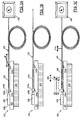
- Figures 1A to 1F are extremely schematic views of some of the relevant steps of a manufacturing method according to a first embodiment of the present invention, applied to the production and packaging of an HDBR laser;
- Figure 2 shows, in axonometric view, one of the steps of the manufacturing method;
- Figures 3A to 3F are extremely schematic views of some of the relevant steps of a manufacturing method according to a second embodiment of the present invention, applied again to the production and packaging of an HDBR laser;
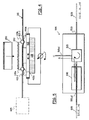
- Figure 4 is an extremely schematic view of a manufacturing method according to a third embodiment of the present invention, applied to the production and packaging of a different type of optical device including a Bragg grating, particularly a wavelength-selective optical filter; and
- Figure 5 is a schematic diagram of an optical subsystem in which the optical device of Figure 4 can be used.
- In Figures 1A to 1F and 2 there are schematically shown some of the relevant steps of a manufacturing method according to a first embodiment of the present invention, for the production, up to the packaging, of an optical device including a Bragg grating. In particular, the first embodiment of the invention described relates to the packaging of an HDBR laser.
- Making reference to the drawings, an Optical SubAssembly (OSA) 100 includes a
semiconductor material chip 105 wherein an optical active element, such as a laser diode, is integrated, attached (typically, bonded), in correspondence of a respective seat, to anOSA support substrate 110, in a material having sufficiently high thermal conductivity properties, for example of silicon or other semiconductors, SiC, diamond, SiGe, GaAs, InP, copper alloys, metals with low thermal expansion properties. - The optical
active element 105, e.g. the laser diode, comprises for example a PN homojunction, such as of GaAs or InP, or alternatively an heterojunction, such as InP/InGaAsP. By way of example, a GaAs laser can be used in applications that provide for exploiting the first attenuation window of optical fibers, corresponding to wavelengths in the range 0.8 to 0.9 µm; a InP/InGaAsP laser can instead operate in the second and third optical fiber attenuation windows , corresponding to wavelengths of about 1.3 to 1.55 µm. However, the invention is not thus limited, applying as well to emitting sources operating at a shorter wavelength (UV or visible spectrum) or at longer one (near or far IR). - The optical
active element 105 has a first and a secondopposite facets first facet 105a is an optically reflecting facet (the chip facet is coated by a film of reflecting material), whereas thesecond facet 105b is only partially reflecting (the chip facet is coated by a film of low-reflectivity or anti-reflecting material) and forms an output port for the optical radiation. - The optical
active element 105 is further provided with electrical terminals (not shown in the drawings for the sake of clarity) for applying a bias and modulation current I for the laser diode. - In order to form a HDBR laser, the
laser diode 105 is coupled to an external optical waveguide, particularly anoptical fiber 115 in a section of which a Bragggrating 120 is formed. In particular, the second, partially-reflectingfacet 105b of the opticalactive element 105 is in optical coupling relationship with aninput termination 115a of thefiber 115, proximate to which the Bragggrating 120 is located. - Techniques for forming Bragg gratings in optical waveguides, particularly optical fibers are known in the art, and are not limitative to the present invention.
- Preferably, the Bragg
grating 120 is realized according to the teachings provided in the already cited WO 01/91259, which is included herein by reference; in such a way, a HDBR laser capable of being directly modulated at high frequency can be obtained. However, it is intended that the Bragg grating might as well be realized in different ways, not being per-se a limitation for the present invention. - Preferably, the
input termination 115a of thefiber 115 is treated so as to form a lens, which allows enhancing the optical coupling to thefacet 105b of the opticalactive element 105. - The OSA
support substrate 110 is mounted to a thermal regulation element, e.g. apeltier cell 125, for stabilizing the temperature of the OSA, particularly of the opticalactive element 105 and the Bragggrating 120, with the purpose of reducing or eliminating thermal drifts of the two critical elements of the OSA. - According to the first embodiment of the invention being described, the optical
active element 105 is first attached (bonded) to theOSA support substrate 110. Then, thefiber 115 is positioned on theOSA support substrate 110, having care to ensure the precise alignment, and the distance of thefiber input termination 115a with respect to the radiation-emitting,second facet 105b of theelement 105, so as to ensure good optical coupling. To this purpose, as schematically depicted in Figure 1A, the optical power coupled into thefiber 115 may be measured, by asuitable instrument 130, for example an optical power meter connected to an output termination of thefiber 115. While thefiber 115 is moved on theOSA substrate 110 with respect to the opticalactive element 105, the optical power emitted by the latter and coupled into the fiber is monitored by theoptical power meter 130; the correct positioning of thefiber 115 is considered achieved when the target optical power is measured by theinstrument 130. - Once the
fiber 115 has been correctly positioned, thefiber 115 is attached to theOSA support substrate 110 at a first attachment point. In particular, as shown in Figure 1B, thefiber 115 is attached, e.g. bonded bysolder 135a, to the OSA support substrate surface at a firstfiber bonding site 110a, for example a metallization provided on thesubstrate 110. Thefiber 115 is preferably bonded to thesubstrate 110 in a region intermediate between theinput termination 115a and the Bragggrating 120. For example, in order to bond the fiber to thesubstrate 110, as described in WO 01/91259, thefiber 115 may be externally metallized in a fiber section region including the fiber attachment region, for example in the fiber section from the input termination to the Bragg grating; in correspondence of thesubstrate bonding site 110a, a micro-heater may be integrated, e.g. a resistor (not shown in the drawings); after the fiber has been properly positioned in the way previously described, the micro-heater is energized so as to generate, for example by Joule effect, sufficient heat to cause reflow or reliquification of the solder alloy that bonds the fiber to the substrate. Other attachment techniques are however possible, the way the fiber is attached to be substrate not being a limitation for the present invention. - In this way, a HDBR laser emitting the desired optical power is obtained; the emission spectrum is relatively narrow, a peculiarity of this type of lasers; the emission wavelength is determined by the frequency response of the Bragg grating in a stressed condition that corresponds to a substantially zero stress, i.e. such a wavelength corresponds to the reflection wavelength of the Bragg grating in a substantially zero-stress condition.
- In order to tune the laser emission wavelength to the desired value, particularly according to the ITU wavelengths grid, which may, and typically does, differ from the above-mentioned substantially zero-stress emission wavelength, the Bragg
grating 120 is applied a controlled stress; in particular, as schematically shown in Figure 1C, thefiber 115 is applied an axial stress STR from the side opposite theinput termination 115a by properly pushing or pulling the fiber, e.g. by hand or in automated way ; this causes the fiber section wherein the Bragggrating 120 is formed to be either stretched, in case the axial stress STR is a tensile, extension stress, or compressed, in case the axial stress STR is a compressive stress. While thefiber 115 is applied the stress STR, the emission wavelength of the HDBR laser is monitored, using asuitable instrument 140, such as a spectrum analyzer connected to the output termination of thefiber 115. The axial stress applied to thefiber 115 varies the position of the equivalent mirror EM of the Bragg grating with respect to thefacet 105a of the opticalactive device 105; in particular, an extension stress causes a shift of the wavelength towards the red, while a compressive stress causes the emission wavelength to be shifted towards the blue. - For example, starting from a substantially zero-stress emission wavelength of 1540 nm, by applying an axial stress of approximately 90 N, the emission wavelength may be varied of approximately 1.1 nm, or 7 nm if a tensile stress of 0,4 GPa is applied.
- Once the target emission wavelength is reached, the corresponding stress is "frozen" in the Bragg grating, by attaching the
fiber 115 to theOSA support substrate 110 at a second attachment point. In particular, as shown in Figure 1D, thefiber 115 is attached, e.g. bonded bysolder 135b, to the OSA support substrate surface at a secondfiber bonding site 110b, e.g. a metallization provided on thesubstrate 110. Thefiber 115 is preferably bonded to thesubstrate 110 in a region downstream (coming from the input termination) the fiber section in which the Bragg grating 120 is formed. The bonding technique may for example be the same described in the foregoing, in connection with the first bonding. - Having thus frozen into the Bragg grating the stress required to achieve the target emission wavelength, by attachment, particularly bonding the
fiber 115 to the OSA, in the two attachment points, it is ensured that the stress applied to the fiber is maintained during time, and that the Bragg grating is kept in the corresponding stress condition, so that the precision of the emission wavelength in time is guaranteed. - However, variations in the operating temperature, particularly the temperature of the Bragg grating, may cause the emission wavelength to change in time.
- Temperature variations of the OSA, particularly of the Bragg grating 120 are reduced by the thermal regulation element, e.g. the
peltier cell 125. - However, the Applicant has observed that in some cases it might be preferable to improve the thermal regulation capabilities of the
peltier cell 125. Thus, as schematically shown in Figures 1E and 2, a cover or cap 150 of a thermally-conductive material, e.g. made of silicon or other semiconductors, or of metals, is provided, of shape and dimensions such that thecap 150 can be placed astride of thefiber 115, so as to preferably span for substantially the whole length of the fiber section containing the Bragg grating 120. Thecap 150, having for example a "C"-shaped cross-section, is attached, preferably bonded to theOSA substrate 110 at two preferably elongatedbonding areas fiber bonding sites cap 150, being of thermally-conductive material and being in thermal contact with thesubstrate 110, which in turn is thermally-regulated by thepeltier cell 125, ensures that, in operation, the temperature of the Bragg grating 120 is kept substantially constant, irrespective of temperature variations in the environment surrounding the Bragg grating. - The
OSA 100 may at this point be placed in arespective package 155, as schematically shown in Figure 1F. Thepackage 155 may for example be in a suitable metal material (for example in KOVAR), preferably exhibiting good properties of heat dissipation, but scarcely dilatable with increase of temperature. Thepackage 155 has ahollow bottom 160, adapted to accommodate theOSA 100 and provided with alateral passage 165 for theoptical fiber 115, and acover 170.Reophores 175 protrude from the package, the ends thereof internal to the package being electrically connected to electric terminals of the OSA 100 (not shown for the sake of clarity). - Thanks to the provision of the
cap 150, even though the Bragg grating 120 is positioned relatively far away from thepeltier cell 125, close to thepackage cover 170, the heat originated outside thepackage 155, possibly flowing thereinto, does not substantially affect the frequency response of the Bragg grating, whose operating temperature is kept regulated by the fact that thecap 150 is thermally-conductive, and is placed in thermal contact with thesubstrate 110, in turn thermally-stabilized by thethermal regulation element 125. Thecap 150 acts in other words as a thermal shield for the Bragg grating 120. - It is observed that the
OSA support substrate 110 might as well be mounted onto thepeltier cell 125 at the time theOSA 100 is inserted into thepackage 155, instead than before. - Another embodiment of the present invention is presented in Figures 3A to 3F. Differently from the previously described embodiment, an
OSA 300 comprises a first and a second OSA support substrates 310-1 and 310-2, which, similarly to theOSA support substrate 110 of the previous embodiment, are made of a material having sufficiently high thermal conductivity properties, for example of silicon or other materials, as mentioned previously. The opticalactive element 105 is attached, e.g. bonded to the first OSA substrate 310-1; the first OSA substrate 310-1 includes, in addition to the bonding area for the chip of the opticalactive element 105, a firstfiber bonding site 310a, intended for bonding thefiber 115. The second OSA substrate 310-2 includes a secondfiber bonding site 310b for bonding thefiber 115; the first and secondfiber bonding sites - The first and second OSA substrates 310-1 and 310-2 are soldered to a
common substrate 313, in a thermally-conductive material. In particular, thecommon substrate 313 is made of a controllably deformable material, particularly a piezoelectric material, and is provided with a first and asecond electrodes common substrate 313, so as to induce therein a controlled deformation. - The
fiber 115 is first positioned having care to ensure the precise alignment, and the distance of thefiber input termination 115a with respect to the radiation-emitting,second facet 105b of theelement 105, so as to ensure good optical coupling. As in the first embodiment described before, the optical power coupled into thefiber 115 may be measured by asuitable instrument 130, for example an optical power meter connected to an output termination of thefiber 115. While thefiber 115 is moved on theOSA substrate 110 with respect to the opticalactive element 105, the optical power emitted by the latter and coupled into the fiber is monitored by theoptical power meter 130; the correct positioning of thefiber 115 is considered achieved when the target optical power is measured by theinstrument 130. - Once the
fiber 115 has been correctly positioned, it is attached to the first OSA substrate 310-1 at a first attachment point. In particular, as shown in Figure 3C, thefiber 115 is attached, e.g. bonded bysolder 135a, to the first OSA substrate 310-1 at the firstfiber bonding site 310a, preferably in a region of the fiber intermediate between theinput termination 115a and the Bragg grating 120. The bonding may for example be accomplished in the way described in the foregoing. - Two exemplary procedures are presented hereinafter that are adapted to tune the emission wavelength of the laser.
- A first tuning procedure calls for attaching, e.g. bonding (by solder) 135b the
fiber 115 to the second OSA substrate 310-2, at the secondfiber bonding site 310b in an initial stress condition of substantially zero stress, without controlling the emission wavelength before attaching the fiber, but having care to ensure that the piezoelectric materialcommon substrate 313 is not in either one of the two full-scale conditions (i.e., maximum extension or maximum contraction); this can for example be done by applying to the piezoelectric common substrate 313 a suitable voltage V through theelectrodes fiber 115 at the second point. Thus, the substantially zero-stress condition of the Bragg grating 120 corresponds to a deformation state of thecommon substrate 313 that is intermediate to the full-scale deformation conditions of the piezoelectric material. At a later stage, possibly directly in use, the emission wavelength of the laser can be tuned by properly biasing thecommon substrate 313, applying to the common substrate 313 a voltage higher or lower than the voltage V corresponding to the initial zero-stress condition of the Bragg grating, so as to vary the position of the Bragg grating equivalent mirror and thus tune the emission wavelength of the laser. - A second tuning procedure calls for preliminarily bringing the deformable
common substrate 313 of piezoelectric material to a selected one of the two opposite full-scale deformation conditions, i.e. maximum extension or maximum contraction; this can be done by applying to the common substrate 313 a suitable voltage V, through theelectrodes fiber 115 at the second point, it is ensured that the laser emission wavelength is slightly lower (in case (a)) or slightly higher (in case (b)) than the target wavelength, e.g. the center-band wavelength of the selected ITU channel. This can be done by monitoring the emission wavelength of the laser by means of a suitable instrument, e.g. thespectrum analyzer 140, and if necessary, applying a controlled (axial) stress to thefiber 115, thus to the Bragg grating 120. Thefiber 115 is then bonded 135b to thesecond bonding site 310a. In this way, the emission wavelength of the laser can be tuned even at a later time, possible in use, by applying a suitable voltage to the piezoelectriccommon substrate 313. In particular, in case (a), by applying to the piezoelectric material a voltage V higher than zero, thecommon substrate 313 is caused to extend, thus a shift of the laser emission wavelength towards the red is achieved; in case (b), by applying to the piezoelectric material a voltage V lower than the maximum voltage, the extension of thecommon substrate 313 is reduced, thus a shift towards the blue of the emission wavelength is achieved. - Referring to Figure 3D, as in the first embodiment described, the thermally-
conductive cap 150 is preferably provided, positioned astride the fiber section in which the Bragg grating is formed, and it is attached, preferably bonded to thecommon substrate 313, for example at twoelongated bonding areas fiber bonding sites cap 150, being of thermally-conductive material and being in thermal contact with thecommon substrate 313, which in turn is thermally-regulated by thepeltier cell 125, ensures that, in operation, the temperature of the Bragg grating 120 is kept substantially constant, irrespective from temperature variations in the environment surrounding the Bragg grating. - The
OSA 300 may at this point be placed in therespective package 155, as schematically shown in Figures 3E and 3F. Two 175a, 175b of thereophores 175 that protrude from the package are in this case connected to theelectrodes common substrate 313, so as to enable finely tuning the laser emission wavelength directly by the user. - Compared to the first embodiment described, this second embodiment offers the possibility of tuning the emission wavelength directly by the user, while preserving the precision and stability over time properties.
- The invention embodiments described so far have made reference to an HDBR laser, including an active optical device such as a laser diode.
- The present invention is not limited to this kind of application, being instead in general applicable to optical devices including a Bragg grating whose wavelength needs to be tuned and made stable.
- For example, in Figure 4 there is schematically shown a different
optical device 400, including anoptical fiber span 115 in which a Bragg grating 120 is formed. Similarly to the second embodiment described in the foregoing, two substrates 410-1 and 410-2 are provided, attached to acommon substrate 413 of controllably deformable material, particularly a slab of piezoelectric material. The two substrates 410-1 and 410-2 include each a respectivefiber bonding site common substrate 413 has two electrodes 415a and 415b through which a voltage can be applied to thecommon substrate 413 so as to induce deformation thereof. - The packaging of the
optical device 400 can proceed as described in connection with the second embodiment; in order to monitor the optical device emission wavelength, an externaloptical source 405 may be used. - Preferably, the provision of the thermally-
conductive cap 150 ensures thermal stability of the Bragg grating. - The
optical device 400 can for example be used in anoptical receiver 500, schematically depicted in terms of functional blocks in Figure 5, for the use e.g. in a WDM optical communications system. Thereceiver 500 has aninput port 510i connected to anoptical communication line 505 of the optical communication system, a first output port 510o1 for connection to a local branch of the communication system, e.g. a local user equipment or a local sub-network, and a second output port 510o2 for the connection to theoptical communication line 505. Through theinput port 510i, a multiple wavelength optical signal, e.g. a WDM signal, is fed to anoptical circulator 515. Between a first output of theoptical circulator 515 and the second output port 510o2 of the receiver there is inserted theoptical device 400, that acts as a wavelength-selective filter, reflecting back optical signals (centered around) a selected (center) wavelength λi. The reflected signal is returned to theoptical circulator 515, and is outputted through the first output port 510o1, while the remaining component signals of the WDM signal, at different wavelengths, are passed through thedevice 400 and returned to theoptical communication line 505. Thanks to the invention embodiment described in the foregoing in connection with Figure 4, thedevice 400 can be made tunable, e.g. by acting on the piezoelectric material of thecommon substrate 413; it is thus possible to realize a tunable optical receiver, that can be tuned onto the desired wavelength λi . - Although the present invention has been disclosed and described by way of some embodiments, it is apparent to those skilled in the art that several modifications to the described embodiments, as well as other embodiments of the present invention are possible without departing from the scope thereof as defined in the appended claims.
Claims (24)
- A method of producing an optical device including a Bragg grating (120) formed in an optical waveguide (115), the method comprising:providing a support substrate (110;310-1,310-2,113;410-1,410-2,413);positioning the optical waveguide on the substrate with respect to an optical source (105;405) so as to achieve a desired optical coupling of optical power emitted by the optical source into the optical waveguide;attaching the waveguide to the support substrate (110a,135a;310a,135a;410a,410b) in correspondence of a first location along the waveguide, said first location being at one side of the Bragg grating;attaching the waveguide to the support substrate (110b,135b;310b,135b) in a correspondence of a second location along the waveguide, said second location being at an opposite side of the Bragg grating, so as to block the Bragg grating in a first stressed condition.
- The method according to claim 1, in which said attaching comprises:providing a first and a second solder-wettable areas (110a,110;310a,310b) on said support substrate;providing solder-wettable areas at said first and second locations along the waveguide;bonding by soldering the solder-wettable area at the first location along the waveguide to the first solder-wettable area on the support substrate, and the solder-wettable area at the second location along the waveguide to the second solder-wettable area on the support substrate.
- The method according to claim 1 or 2, further comprising:applying a stress to the Bragg grating so as to vary a frequency response thereof.
- The method according to claim 3, in which said applying a stress to the Bragg grating includes applying a mechanical stress to the waveguide.
- The method according to claim 4, in which said applying a stress is performed before attaching the waveguide to the support substrate in a correspondence of the second location along the waveguide, and the Bragg grating is blocked in the first stressed condition when a target frequency response is attained.
- The method according to claim 3 or 4, in which said applying a mechanical stress to the waveguide include deforming the support substrate (313;413).
- The method according to claim 6, in which said applying a mechanical stress to the waveguide is performed after attaching the waveguide to the support substrate in a correspondence of the second location along the waveguide, so as to vary the frequency response of the Bragg grating with respect to the frequency response corresponding to the first stress condition, and keeping the Bragg grating in a second stressed condition when a target frequency response is attained.
- The method according to claim 7, in which the first stressed condition is such that the Bragg grating frequency response is slightly different from the target frequency response, and with the support substrate in either one of two full-scale deformation conditions.
- The method according to any one of the preceding claims, further comprising:providing the support substrate with thermal conduction properties; andthermally-stabilizing (125) the support substrate.
- The method according to claim 9, further comprising:thermally shielding (125) the Bragg grating.
- The method according to claim 10, in which said thermally shielding comprises:providing an enclosure (150) around the Bragg grating, said enclosure being thermally conductive and being in thermal conduction relationship with the thermally-stabilized support substrate.
- An optical device comprising:an optical waveguide (115),a Bragg grating (120) formed in the waveguide;a support substrate (110;310-1,310-2,113;410-1,410-2,413),
characterized by comprising:a first and a second waveguide attachment locations, at which the waveguide is attached to the support substrate, said first and second attachment locations being located at opposite side with respect to the Bragg grating, so as to block the Bragg grating in a first stressed condition. - The optical device according to claim 12, in which said support substrate (313;413) is controllably deformable, a deformation of the substrate causing a stress applied to the Bragg grating that induces a change in a frequency response thereof.
- The optical device according to claim 13, in which said support substrate comprises:a first substrate (310-1;410-1) including said first waveguide attachment location;a second substrate (310-2;410-2) including said second waveguide attachment location, anda common substrate (313;413) to which the first and second substrates are attached, the common substrate being of a controllably deformable material.
- The optical device according to claim 14, in the common substrate is in a piezoelectric material.
- The optical device according to any one of claims 11 to 15, in which the support substrate is thermally conductive, and is associated with a thermal stabilizer (125) adapted to substantially stabilize a temperature of the substrate.
- The optical device according to claim 16, further comprising a thermal shield (125) for the Bragg grating.
- The optical device according to claim 17, in which said thermal shield comprises thermally conductive enclosure (150) surrounding the Bragg grating, said enclosure being in thermal conduction relationship with the thermally-stabilized support substrate.
- The optical device according to any one of claims 12 to 18, further comprising an optical source (105) optically coupled to the waveguide.
- The optical device according to claim 19, in which said optical source includes a laser diode.
- A method of tuning an optical device including a Bragg grating (120) formed in an optical waveguide (115), the method comprising:providing a support substrate (110;310-1,310-2,113;410-1,410-2,413);positioning the optical waveguide on the substrate with respect to an optical source (105;405) so as to achieve a desired optical coupling of optical power emitted by the optical source into the optical waveguide;attaching the waveguide to the support substrate (110a,135a;310a,135a;410a,410b) in correspondence of a first location along the waveguide, said first location being at one side of the Bragg grating;attaching the waveguide to the support substrate (110b,135b;310b,135b) in a correspondence of a second location along the waveguide, said second location being at an opposite side of the Bragg grating;wherein a stress is applied to the Bragg grating so as to vary a frequency response thereof.
- The method according to claim 21, in which said stress is applied to the Bragg grating before said attaching the waveguide to the support substrate (110b,135b;310b,135b) in a correspondence of a second location along the waveguide.
- The method according to claim 21, in which said stress is applied to the Bragg grating after said attaching the waveguide to the support substrate (110b,135b;310b,135b) in a correspondence of a second location along the waveguide.
- A tunable optical device including:an optical waveguide (115),a Bragg grating (120) formed in the waveguide;a support substrate (110;310-1,310-2,113;410-1,410-2,413),
characterized in that:a first and a second waveguide attachment locations are provided, at which the waveguide is attached to the support substrate, said first and second attachment locations being located at opposite side with respect to the Bragg grating;
and in thatthe support substrate includes a controllably deformable material substrate (413), adapted to be controllably deformed so as to controllably vary a stress condition of the Bragg grating, whereby a frequency response of the optical device can be tuned.
Priority Applications (2)
| Application Number | Priority Date | Filing Date | Title |
|---|---|---|---|
| EP04103032A EP1617244A1 (en) | 2004-06-29 | 2004-06-29 | Optical device including a Bragg grating and method of manufacturing thereof |
| US11/172,384 US20060023999A1 (en) | 2004-06-29 | 2005-06-29 | Manufacturing of optical devices including bragg gratings |
Applications Claiming Priority (1)
| Application Number | Priority Date | Filing Date | Title |
|---|---|---|---|
| EP04103032A EP1617244A1 (en) | 2004-06-29 | 2004-06-29 | Optical device including a Bragg grating and method of manufacturing thereof |
Publications (1)
| Publication Number | Publication Date |
|---|---|
| EP1617244A1 true EP1617244A1 (en) | 2006-01-18 |
Family
ID=34929266
Family Applications (1)
| Application Number | Title | Priority Date | Filing Date |
|---|---|---|---|
| EP04103032A Withdrawn EP1617244A1 (en) | 2004-06-29 | 2004-06-29 | Optical device including a Bragg grating and method of manufacturing thereof |
Country Status (2)
| Country | Link |
|---|---|
| US (1) | US20060023999A1 (en) |
| EP (1) | EP1617244A1 (en) |
Cited By (1)
| Publication number | Priority date | Publication date | Assignee | Title |
|---|---|---|---|---|
| EP2709218A3 (en) * | 2012-09-13 | 2014-06-04 | Northrop Grumman Guidance and Electronics Company, Inc. | Stabilized pump laser output system and method |
Families Citing this family (3)
| Publication number | Priority date | Publication date | Assignee | Title |
|---|---|---|---|---|
| US11005233B2 (en) * | 2016-08-22 | 2021-05-11 | Morton Hybrid Lasers, Llc | Ultra-low noise, highly stable single-mode operation, high power, Bragg grating based semiconductor laser |
| CN111725689A (en) * | 2020-05-29 | 2020-09-29 | 中国科学院上海光学精密机械研究所 | Narrow Linewidth Fast Tuning Laser |
| FR3155911A1 (en) * | 2023-11-24 | 2025-05-30 | Safran | OPTICAL SPECTRUM MODULATOR DEVICE |
Citations (9)
| Publication number | Priority date | Publication date | Assignee | Title |
|---|---|---|---|---|
| WO1999027400A2 (en) * | 1997-11-24 | 1999-06-03 | Ionas A/S | Temperature stabilization of optical waveguides |
| WO2001035133A1 (en) * | 1999-11-11 | 2001-05-17 | Koheras A/S | Compact athermal optical waveguide using thermal expansion amplification |
| EP1104055A2 (en) * | 1995-11-01 | 2001-05-30 | Sumitomo Electric Industries, Ltd. | Laser light source apparatus and OTDR apparatus |
| US6347175B1 (en) * | 1999-07-14 | 2002-02-12 | Corning Incorporated | Solderable thin film |
| US6393181B1 (en) * | 1997-06-19 | 2002-05-21 | Jds Uniphase Pty. Ltd. | Temperature stable Bragg grating package with post tuning for accurate setting of centre frequency |
| US20020154883A1 (en) * | 2000-02-07 | 2002-10-24 | Francois Seguin | Bonding optical fibers to substrates |
| US6480513B1 (en) * | 2000-10-03 | 2002-11-12 | K2 Optronics, Inc. | Tunable external cavity laser |
| US20030016909A1 (en) * | 2001-05-15 | 2003-01-23 | Atsushi Shinozaki | Optical module |
| US20030123800A1 (en) * | 2001-12-27 | 2003-07-03 | Minoru Hashimoto | Variable dispersion compensator and substrate for the same |
Family Cites Families (2)
| Publication number | Priority date | Publication date | Assignee | Title |
|---|---|---|---|---|
| JPH10206753A (en) * | 1997-01-28 | 1998-08-07 | Nec Corp | Variable wavelength optical device |
| US6360042B1 (en) * | 2001-01-31 | 2002-03-19 | Pin Long | Tunable optical fiber gratings device |
-
2004
- 2004-06-29 EP EP04103032A patent/EP1617244A1/en not_active Withdrawn
-
2005
- 2005-06-29 US US11/172,384 patent/US20060023999A1/en not_active Abandoned
Patent Citations (9)
| Publication number | Priority date | Publication date | Assignee | Title |
|---|---|---|---|---|
| EP1104055A2 (en) * | 1995-11-01 | 2001-05-30 | Sumitomo Electric Industries, Ltd. | Laser light source apparatus and OTDR apparatus |
| US6393181B1 (en) * | 1997-06-19 | 2002-05-21 | Jds Uniphase Pty. Ltd. | Temperature stable Bragg grating package with post tuning for accurate setting of centre frequency |
| WO1999027400A2 (en) * | 1997-11-24 | 1999-06-03 | Ionas A/S | Temperature stabilization of optical waveguides |
| US6347175B1 (en) * | 1999-07-14 | 2002-02-12 | Corning Incorporated | Solderable thin film |
| WO2001035133A1 (en) * | 1999-11-11 | 2001-05-17 | Koheras A/S | Compact athermal optical waveguide using thermal expansion amplification |
| US20020154883A1 (en) * | 2000-02-07 | 2002-10-24 | Francois Seguin | Bonding optical fibers to substrates |
| US6480513B1 (en) * | 2000-10-03 | 2002-11-12 | K2 Optronics, Inc. | Tunable external cavity laser |
| US20030016909A1 (en) * | 2001-05-15 | 2003-01-23 | Atsushi Shinozaki | Optical module |
| US20030123800A1 (en) * | 2001-12-27 | 2003-07-03 | Minoru Hashimoto | Variable dispersion compensator and substrate for the same |
Non-Patent Citations (2)
| Title |
|---|
| PAOLETTI R.; MELIGA M.: "HDBR (Hybrid Distributed Bragg Reflector) for WDM and OTDM applications", PROCEEDINGS OF SPIE, CONFERENCE ON PHYSICS AND SIMULATION OF OPTOELECTRONIC DEVICES IX, vol. 4283, 22 January 2001 (2001-01-22), pages 355 - 366 * |
| PSAILA D.C.; INGLIS H.G.: "Packaging of Optical Fibre Bragg Gratings", PROCEEDINGS OF 51ST ELECTRONIC COMPONENTS AND TECHNOLOGY CONFERENCE 2001, 29 May 2001 (2001-05-29), pages 439 - 443 * |
Cited By (2)
| Publication number | Priority date | Publication date | Assignee | Title |
|---|---|---|---|---|
| EP2709218A3 (en) * | 2012-09-13 | 2014-06-04 | Northrop Grumman Guidance and Electronics Company, Inc. | Stabilized pump laser output system and method |
| US9031366B2 (en) | 2012-09-13 | 2015-05-12 | Northrop Grumman Guidance And Electronic Company, Inc. | Stabilized pump laser output system and method |
Also Published As
| Publication number | Publication date |
|---|---|
| US20060023999A1 (en) | 2006-02-02 |
Similar Documents
| Publication | Publication Date | Title |
|---|---|---|
| US8483247B2 (en) | Thermally controlled external cavity tuneable laser | |
| EP2095476B1 (en) | Phase control by active thermal adjustments in an external cavity laser | |
| US8259765B2 (en) | Passive phase control in an external cavity laser | |
| US7570675B2 (en) | Liquid crystal polymer optical filter carrier | |
| CN111146683A (en) | Tunable laser device based on silicon photons and packaging structure thereof | |
| KR102237784B1 (en) | Laser Device with wavelength stabilizer | |
| US7295582B2 (en) | Thermo-optic tunable laser apparatus | |
| US20020186729A1 (en) | Optical module, transmitter and WDM transmitting device | |
| US11848539B2 (en) | Narrow linewidth semiconductor laser device | |
| CN104350652B (en) | Laser device with wavelength stabilizing device | |
| US10084284B2 (en) | Light emitting device with extended mode-hop-free spectral tuning ranges and method of manufacture | |
| US7869475B2 (en) | Misalignment prevention in an external cavity laser having temperature stabilisation of the resonator and the gain medium | |
| US20060023999A1 (en) | Manufacturing of optical devices including bragg gratings | |
| EP1285480B1 (en) | External cavity laser | |
| EP1958302B1 (en) | Passive phase control in an external cavity laser | |
| KR20070028463A (en) | Thermally Controlled External Cavity Laser | |
| US20260039086A1 (en) | Ultra Small Packaged Tunable Laser Assembly | |
| CN118054299A (en) | Ultra-small packaged tunable laser assembly | |
| JPH11103121A (en) | Semiconductor laser |
Legal Events
| Date | Code | Title | Description |
|---|---|---|---|
| PUAI | Public reference made under article 153(3) epc to a published international application that has entered the european phase |
Free format text: ORIGINAL CODE: 0009012 |
|
| AK | Designated contracting states |
Kind code of ref document: A1 Designated state(s): AT BE BG CH CY CZ DE DK EE ES FI FR GB GR HU IE IT LI LU MC NL PL PT RO SE SI SK TR |
|
| AX | Request for extension of the european patent |
Extension state: AL HR LT LV MK |
|
| 17P | Request for examination filed |
Effective date: 20060704 |
|
| 17Q | First examination report despatched |
Effective date: 20060731 |
|
| AKX | Designation fees paid |
Designated state(s): DE FR GB IT |
|
| 17Q | First examination report despatched |
Effective date: 20060731 |
|
| GRAP | Despatch of communication of intention to grant a patent |
Free format text: ORIGINAL CODE: EPIDOSNIGR1 |
|
| RIC1 | Information provided on ipc code assigned before grant |
Ipc: H01S 5/14 20060101ALI20080923BHEP Ipc: H01S 5/022 20060101ALI20080923BHEP Ipc: G02B 6/02 20060101ALI20080923BHEP Ipc: G02B 6/42 20060101AFI20080923BHEP |
|
| RTI1 | Title (correction) |
Free format text: METHOD OF MANUFACTURING FOR OPTICAL DEVICE INCLUDING A BRAGG GRATING |
|
| STAA | Information on the status of an ep patent application or granted ep patent |
Free format text: STATUS: THE APPLICATION IS DEEMED TO BE WITHDRAWN |
|
| 18D | Application deemed to be withdrawn |
Effective date: 20090317 |