EP1616217B1 - Electro-optic assemblies - Google Patents
Electro-optic assemblies Download PDFInfo
- Publication number
- EP1616217B1 EP1616217B1 EP04758361A EP04758361A EP1616217B1 EP 1616217 B1 EP1616217 B1 EP 1616217B1 EP 04758361 A EP04758361 A EP 04758361A EP 04758361 A EP04758361 A EP 04758361A EP 1616217 B1 EP1616217 B1 EP 1616217B1
- Authority
- EP
- European Patent Office
- Prior art keywords
- electro
- optic
- adhesive
- layer
- display
- Prior art date
- Legal status (The legal status is an assumption and is not a legal conclusion. Google has not performed a legal analysis and makes no representation as to the accuracy of the status listed.)
- Expired - Lifetime
Links
- 230000000712 assembly Effects 0.000 title description 8
- 238000000429 assembly Methods 0.000 title description 8
- 239000000853 adhesive Substances 0.000 claims abstract description 106
- 230000001070 adhesive effect Effects 0.000 claims abstract description 105
- 239000000463 material Substances 0.000 claims abstract description 63
- 150000003839 salts Chemical class 0.000 claims abstract description 41
- 239000000203 mixture Substances 0.000 claims abstract description 15
- 239000010410 layer Substances 0.000 claims description 88
- 239000012790 adhesive layer Substances 0.000 claims description 55
- 239000000758 substrate Substances 0.000 claims description 43
- 239000007787 solid Substances 0.000 claims description 26
- -1 hexafluorophosphate Chemical compound 0.000 claims description 25
- 230000003287 optical effect Effects 0.000 claims description 17
- 239000000382 optic material Substances 0.000 claims description 16
- SCVFZCLFOSHCOH-UHFFFAOYSA-M potassium acetate Chemical compound [K+].CC([O-])=O SCVFZCLFOSHCOH-UHFFFAOYSA-M 0.000 claims description 15
- 238000004519 manufacturing process Methods 0.000 claims description 12
- NHGXDBSUJJNIRV-UHFFFAOYSA-M tetrabutylammonium chloride Chemical compound [Cl-].CCCC[N+](CCCC)(CCCC)CCCC NHGXDBSUJJNIRV-UHFFFAOYSA-M 0.000 claims description 11
- 235000011056 potassium acetate Nutrition 0.000 claims description 6
- 239000003086 colorant Substances 0.000 claims description 5
- 229920002635 polyurethane Polymers 0.000 claims description 5
- 239000004814 polyurethane Substances 0.000 claims description 5
- 150000003242 quaternary ammonium salts Chemical class 0.000 claims description 5
- 150000005621 tetraalkylammonium salts Chemical class 0.000 claims description 3
- 239000000654 additive Substances 0.000 abstract description 45
- 230000000996 additive effect Effects 0.000 abstract description 34
- 239000002245 particle Substances 0.000 abstract description 18
- 239000002775 capsule Substances 0.000 abstract description 17
- 230000005684 electric field Effects 0.000 abstract description 10
- 239000011230 binding agent Substances 0.000 abstract description 9
- 239000012530 fluid Substances 0.000 abstract description 7
- 229920000867 polyelectrolyte Polymers 0.000 abstract 1
- 239000005518 polymer electrolyte Substances 0.000 abstract 1
- 239000007784 solid electrolyte Substances 0.000 abstract 1
- 238000003475 lamination Methods 0.000 description 58
- 238000000034 method Methods 0.000 description 31
- 239000010408 film Substances 0.000 description 23
- 238000000576 coating method Methods 0.000 description 19
- 239000011248 coating agent Substances 0.000 description 16
- 230000008569 process Effects 0.000 description 15
- 238000012360 testing method Methods 0.000 description 11
- 230000008859 change Effects 0.000 description 7
- 239000004973 liquid crystal related substance Substances 0.000 description 7
- 239000000975 dye Substances 0.000 description 6
- 239000011159 matrix material Substances 0.000 description 6
- 239000004816 latex Substances 0.000 description 5
- 229920000126 latex Polymers 0.000 description 5
- 239000007788 liquid Substances 0.000 description 5
- 229920003023 plastic Polymers 0.000 description 5
- 229920000139 polyethylene terephthalate Polymers 0.000 description 5
- 239000005020 polyethylene terephthalate Substances 0.000 description 5
- 229920000642 polymer Polymers 0.000 description 5
- 239000000523 sample Substances 0.000 description 5
- JOYRKODLDBILNP-UHFFFAOYSA-N Ethyl urethane Chemical compound CCOC(N)=O JOYRKODLDBILNP-UHFFFAOYSA-N 0.000 description 4
- PXHVJJICTQNCMI-UHFFFAOYSA-N Nickel Chemical compound [Ni] PXHVJJICTQNCMI-UHFFFAOYSA-N 0.000 description 4
- 230000000694 effects Effects 0.000 description 4
- 238000010030 laminating Methods 0.000 description 4
- 239000003094 microcapsule Substances 0.000 description 4
- 238000002156 mixing Methods 0.000 description 4
- 239000004033 plastic Substances 0.000 description 4
- 239000002985 plastic film Substances 0.000 description 4
- 238000007639 printing Methods 0.000 description 4
- 239000000243 solution Substances 0.000 description 4
- 239000007864 aqueous solution Substances 0.000 description 3
- 239000006185 dispersion Substances 0.000 description 3
- 239000000839 emulsion Substances 0.000 description 3
- AMGQUBHHOARCQH-UHFFFAOYSA-N indium;oxotin Chemical compound [In].[Sn]=O AMGQUBHHOARCQH-UHFFFAOYSA-N 0.000 description 3
- 229920006255 plastic film Polymers 0.000 description 3
- 229920003009 polyurethane dispersion Polymers 0.000 description 3
- 239000002243 precursor Substances 0.000 description 3
- 239000011241 protective layer Substances 0.000 description 3
- XLYOFNOQVPJJNP-UHFFFAOYSA-N water Substances O XLYOFNOQVPJJNP-UHFFFAOYSA-N 0.000 description 3
- 229920002799 BoPET Polymers 0.000 description 2
- 239000004593 Epoxy Substances 0.000 description 2
- 239000004721 Polyphenylene oxide Substances 0.000 description 2
- CDBYLPFSWZWCQE-UHFFFAOYSA-L Sodium Carbonate Chemical compound [Na+].[Na+].[O-]C([O-])=O CDBYLPFSWZWCQE-UHFFFAOYSA-L 0.000 description 2
- 229920002125 Sokalan® Polymers 0.000 description 2
- XTXRWKRVRITETP-UHFFFAOYSA-N Vinyl acetate Chemical compound CC(=O)OC=C XTXRWKRVRITETP-UHFFFAOYSA-N 0.000 description 2
- 229910052782 aluminium Inorganic materials 0.000 description 2
- XAGFODPZIPBFFR-UHFFFAOYSA-N aluminium Chemical compound [Al] XAGFODPZIPBFFR-UHFFFAOYSA-N 0.000 description 2
- 239000002585 base Substances 0.000 description 2
- 239000003139 biocide Substances 0.000 description 2
- 230000005540 biological transmission Effects 0.000 description 2
- 230000001427 coherent effect Effects 0.000 description 2
- 239000012612 commercial material Substances 0.000 description 2
- 230000001143 conditioned effect Effects 0.000 description 2
- 239000004020 conductor Substances 0.000 description 2
- 238000001723 curing Methods 0.000 description 2
- 230000007423 decrease Effects 0.000 description 2
- 238000001035 drying Methods 0.000 description 2
- HDERJYVLTPVNRI-UHFFFAOYSA-N ethene;ethenyl acetate Chemical group C=C.CC(=O)OC=C HDERJYVLTPVNRI-UHFFFAOYSA-N 0.000 description 2
- 238000002474 experimental method Methods 0.000 description 2
- 239000000945 filler Substances 0.000 description 2
- 229910017053 inorganic salt Inorganic materials 0.000 description 2
- 229910052759 nickel Inorganic materials 0.000 description 2
- 230000010287 polarization Effects 0.000 description 2
- 229920000570 polyether Polymers 0.000 description 2
- 229920001228 polyisocyanate Polymers 0.000 description 2
- 239000005056 polyisocyanate Substances 0.000 description 2
- 229920005862 polyol Polymers 0.000 description 2
- 150000003077 polyols Chemical class 0.000 description 2
- 229920002981 polyvinylidene fluoride Polymers 0.000 description 2
- 239000011347 resin Substances 0.000 description 2
- 229920005989 resin Polymers 0.000 description 2
- 239000011342 resin composition Substances 0.000 description 2
- 230000000717 retained effect Effects 0.000 description 2
- 239000002904 solvent Substances 0.000 description 2
- 238000003860 storage Methods 0.000 description 2
- DZLFLBLQUQXARW-UHFFFAOYSA-N tetrabutylammonium Chemical compound CCCC[N+](CCCC)(CCCC)CCCC DZLFLBLQUQXARW-UHFFFAOYSA-N 0.000 description 2
- 210000003934 vacuole Anatomy 0.000 description 2
- YZTJKOLMWJNVFH-UHFFFAOYSA-N 2-sulfobenzene-1,3-dicarboxylic acid Chemical compound OC(=O)C1=CC=CC(C(O)=O)=C1S(O)(=O)=O YZTJKOLMWJNVFH-UHFFFAOYSA-N 0.000 description 1
- UXVMQQNJUSDDNG-UHFFFAOYSA-L Calcium chloride Chemical compound [Cl-].[Cl-].[Ca+2] UXVMQQNJUSDDNG-UHFFFAOYSA-L 0.000 description 1
- OKTJSMMVPCPJKN-UHFFFAOYSA-N Carbon Chemical compound [C] OKTJSMMVPCPJKN-UHFFFAOYSA-N 0.000 description 1
- 239000004215 Carbon black (E152) Substances 0.000 description 1
- 239000004970 Chain extender Substances 0.000 description 1
- VEXZGXHMUGYJMC-UHFFFAOYSA-M Chloride anion Chemical compound [Cl-] VEXZGXHMUGYJMC-UHFFFAOYSA-M 0.000 description 1
- 229910013131 LiN Inorganic materials 0.000 description 1
- 229910001290 LiPF6 Inorganic materials 0.000 description 1
- 229920000134 Metallised film Polymers 0.000 description 1
- 239000005041 Mylar™ Substances 0.000 description 1
- 239000004983 Polymer Dispersed Liquid Crystal Substances 0.000 description 1
- 239000004820 Pressure-sensitive adhesive Substances 0.000 description 1
- LSNNMFCWUKXFEE-UHFFFAOYSA-N Sulfurous acid Chemical compound OS(O)=O LSNNMFCWUKXFEE-UHFFFAOYSA-N 0.000 description 1
- 241001422033 Thestylus Species 0.000 description 1
- 239000002253 acid Substances 0.000 description 1
- 230000002411 adverse Effects 0.000 description 1
- 238000004220 aggregation Methods 0.000 description 1
- 230000002776 aggregation Effects 0.000 description 1
- 238000013019 agitation Methods 0.000 description 1
- 238000007754 air knife coating Methods 0.000 description 1
- 239000005456 alcohol based solvent Substances 0.000 description 1
- 229910052783 alkali metal Inorganic materials 0.000 description 1
- 150000003863 ammonium salts Chemical class 0.000 description 1
- 229910052921 ammonium sulfate Inorganic materials 0.000 description 1
- 235000011130 ammonium sulphate Nutrition 0.000 description 1
- 239000002216 antistatic agent Substances 0.000 description 1
- QVGXLLKOCUKJST-UHFFFAOYSA-N atomic oxygen Chemical compound [O] QVGXLLKOCUKJST-UHFFFAOYSA-N 0.000 description 1
- 230000001580 bacterial effect Effects 0.000 description 1
- 230000004888 barrier function Effects 0.000 description 1
- 230000003115 biocidal effect Effects 0.000 description 1
- 239000001110 calcium chloride Substances 0.000 description 1
- 229910001628 calcium chloride Inorganic materials 0.000 description 1
- 230000015556 catabolic process Effects 0.000 description 1
- 239000003795 chemical substances by application Substances 0.000 description 1
- 238000004040 coloring Methods 0.000 description 1
- 239000000805 composite resin Substances 0.000 description 1
- 150000001875 compounds Chemical class 0.000 description 1
- 229920001940 conductive polymer Polymers 0.000 description 1
- 239000000470 constituent Substances 0.000 description 1
- 239000013068 control sample Substances 0.000 description 1
- 210000002858 crystal cell Anatomy 0.000 description 1
- 238000007766 curtain coating Methods 0.000 description 1
- 230000007547 defect Effects 0.000 description 1
- 238000006731 degradation reaction Methods 0.000 description 1
- 238000007607 die coating method Methods 0.000 description 1
- 238000003618 dip coating Methods 0.000 description 1
- VVTXSHLLIKXMPY-UHFFFAOYSA-L disodium;2-sulfobenzene-1,3-dicarboxylate Chemical compound [Na+].[Na+].OS(=O)(=O)C1=C(C([O-])=O)C=CC=C1C([O-])=O VVTXSHLLIKXMPY-UHFFFAOYSA-L 0.000 description 1
- 239000002019 doping agent Substances 0.000 description 1
- 238000005516 engineering process Methods 0.000 description 1
- 239000003759 ester based solvent Substances 0.000 description 1
- 150000002148 esters Chemical class 0.000 description 1
- 238000007765 extrusion coating Methods 0.000 description 1
- 239000010419 fine particle Substances 0.000 description 1
- 239000007789 gas Substances 0.000 description 1
- 239000010439 graphite Substances 0.000 description 1
- 229910002804 graphite Inorganic materials 0.000 description 1
- 238000007756 gravure coating Methods 0.000 description 1
- 238000013007 heat curing Methods 0.000 description 1
- 229930195733 hydrocarbon Natural products 0.000 description 1
- 150000002430 hydrocarbons Chemical class 0.000 description 1
- 230000002209 hydrophobic effect Effects 0.000 description 1
- 238000003384 imaging method Methods 0.000 description 1
- 238000011065 in-situ storage Methods 0.000 description 1
- 238000010348 incorporation Methods 0.000 description 1
- 238000007641 inkjet printing Methods 0.000 description 1
- 230000001788 irregular Effects 0.000 description 1
- 150000002576 ketones Chemical class 0.000 description 1
- 238000009685 knife-over-roll coating Methods 0.000 description 1
- 230000000670 limiting effect Effects 0.000 description 1
- 229910001540 lithium hexafluoroarsenate(V) Inorganic materials 0.000 description 1
- 229910003002 lithium salt Inorganic materials 0.000 description 1
- 159000000002 lithium salts Chemical class 0.000 description 1
- 229910001496 lithium tetrafluoroborate Inorganic materials 0.000 description 1
- 230000007774 longterm Effects 0.000 description 1
- 238000004020 luminiscence type Methods 0.000 description 1
- 238000005259 measurement Methods 0.000 description 1
- 239000012528 membrane Substances 0.000 description 1
- 230000005499 meniscus Effects 0.000 description 1
- 229910052751 metal Inorganic materials 0.000 description 1
- 239000002184 metal Substances 0.000 description 1
- 229910044991 metal oxide Inorganic materials 0.000 description 1
- 150000004706 metal oxides Chemical class 0.000 description 1
- 238000000465 moulding Methods 0.000 description 1
- 229910052760 oxygen Inorganic materials 0.000 description 1
- 239000001301 oxygen Substances 0.000 description 1
- 238000005325 percolation Methods 0.000 description 1
- 125000005010 perfluoroalkyl group Chemical group 0.000 description 1
- 239000011574 phosphorus Substances 0.000 description 1
- 229910052698 phosphorus Inorganic materials 0.000 description 1
- 229920001495 poly(sodium acrylate) polymer Polymers 0.000 description 1
- 229920000058 polyacrylate Polymers 0.000 description 1
- 229920000728 polyester Polymers 0.000 description 1
- 229920001296 polysiloxane Polymers 0.000 description 1
- 150000003112 potassium compounds Chemical class 0.000 description 1
- 230000005855 radiation Effects 0.000 description 1
- 238000012827 research and development Methods 0.000 description 1
- 239000012260 resinous material Substances 0.000 description 1
- 238000007763 reverse roll coating Methods 0.000 description 1
- 230000002441 reversible effect Effects 0.000 description 1
- 239000012266 salt solution Substances 0.000 description 1
- 238000007650 screen-printing Methods 0.000 description 1
- 229910000029 sodium carbonate Inorganic materials 0.000 description 1
- NNMHYFLPFNGQFZ-UHFFFAOYSA-M sodium polyacrylate Chemical compound [Na+].[O-]C(=O)C=C NNMHYFLPFNGQFZ-UHFFFAOYSA-M 0.000 description 1
- 159000000000 sodium salts Chemical class 0.000 description 1
- 238000004528 spin coating Methods 0.000 description 1
- 230000002269 spontaneous effect Effects 0.000 description 1
- 238000005507 spraying Methods 0.000 description 1
- 239000011550 stock solution Substances 0.000 description 1
- 239000000126 substance Substances 0.000 description 1
- 238000007651 thermal printing Methods 0.000 description 1
- 239000010409 thin film Substances 0.000 description 1
- DVKJHBMWWAPEIU-UHFFFAOYSA-N toluene 2,4-diisocyanate Chemical compound CC1=CC=C(N=C=O)C=C1N=C=O DVKJHBMWWAPEIU-UHFFFAOYSA-N 0.000 description 1
- DQWPFSLDHJDLRL-UHFFFAOYSA-N triethyl phosphate Chemical compound CCOP(=O)(OCC)OCC DQWPFSLDHJDLRL-UHFFFAOYSA-N 0.000 description 1
- 238000011179 visual inspection Methods 0.000 description 1
- 239000002023 wood Substances 0.000 description 1
Images


Classifications
-
- B—PERFORMING OPERATIONS; TRANSPORTING
- B32—LAYERED PRODUCTS
- B32B—LAYERED PRODUCTS, i.e. PRODUCTS BUILT-UP OF STRATA OF FLAT OR NON-FLAT, e.g. CELLULAR OR HONEYCOMB, FORM
- B32B7/00—Layered products characterised by the relation between layers; Layered products characterised by the relative orientation of features between layers, or by the relative values of a measurable parameter between layers, i.e. products comprising layers having different physical, chemical or physicochemical properties; Layered products characterised by the interconnection of layers
- B32B7/04—Interconnection of layers
- B32B7/06—Interconnection of layers permitting easy separation
-
- G—PHYSICS
- G02—OPTICS
- G02F—OPTICAL DEVICES OR ARRANGEMENTS FOR THE CONTROL OF LIGHT BY MODIFICATION OF THE OPTICAL PROPERTIES OF THE MEDIA OF THE ELEMENTS INVOLVED THEREIN; NON-LINEAR OPTICS; FREQUENCY-CHANGING OF LIGHT; OPTICAL LOGIC ELEMENTS; OPTICAL ANALOGUE/DIGITAL CONVERTERS
- G02F1/00—Devices or arrangements for the control of the intensity, colour, phase, polarisation or direction of light arriving from an independent light source, e.g. switching, gating or modulating; Non-linear optics
- G02F1/01—Devices or arrangements for the control of the intensity, colour, phase, polarisation or direction of light arriving from an independent light source, e.g. switching, gating or modulating; Non-linear optics for the control of the intensity, phase, polarisation or colour
- G02F1/165—Devices or arrangements for the control of the intensity, colour, phase, polarisation or direction of light arriving from an independent light source, e.g. switching, gating or modulating; Non-linear optics for the control of the intensity, phase, polarisation or colour based on translational movement of particles in a fluid under the influence of an applied field
- G02F1/166—Devices or arrangements for the control of the intensity, colour, phase, polarisation or direction of light arriving from an independent light source, e.g. switching, gating or modulating; Non-linear optics for the control of the intensity, phase, polarisation or colour based on translational movement of particles in a fluid under the influence of an applied field characterised by the electro-optical or magneto-optical effect
- G02F1/167—Devices or arrangements for the control of the intensity, colour, phase, polarisation or direction of light arriving from an independent light source, e.g. switching, gating or modulating; Non-linear optics for the control of the intensity, phase, polarisation or colour based on translational movement of particles in a fluid under the influence of an applied field characterised by the electro-optical or magneto-optical effect by electrophoresis
-
- B—PERFORMING OPERATIONS; TRANSPORTING
- B32—LAYERED PRODUCTS
- B32B—LAYERED PRODUCTS, i.e. PRODUCTS BUILT-UP OF STRATA OF FLAT OR NON-FLAT, e.g. CELLULAR OR HONEYCOMB, FORM
- B32B7/00—Layered products characterised by the relation between layers; Layered products characterised by the relative orientation of features between layers, or by the relative values of a measurable parameter between layers, i.e. products comprising layers having different physical, chemical or physicochemical properties; Layered products characterised by the interconnection of layers
- B32B7/04—Interconnection of layers
- B32B7/12—Interconnection of layers using interposed adhesives or interposed materials with bonding properties
-
- C—CHEMISTRY; METALLURGY
- C09—DYES; PAINTS; POLISHES; NATURAL RESINS; ADHESIVES; COMPOSITIONS NOT OTHERWISE PROVIDED FOR; APPLICATIONS OF MATERIALS NOT OTHERWISE PROVIDED FOR
- C09J—ADHESIVES; NON-MECHANICAL ASPECTS OF ADHESIVE PROCESSES IN GENERAL; ADHESIVE PROCESSES NOT PROVIDED FOR ELSEWHERE; USE OF MATERIALS AS ADHESIVES
- C09J11/00—Features of adhesives not provided for in group C09J9/00, e.g. additives
- C09J11/02—Non-macromolecular additives
-
- C—CHEMISTRY; METALLURGY
- C09—DYES; PAINTS; POLISHES; NATURAL RESINS; ADHESIVES; COMPOSITIONS NOT OTHERWISE PROVIDED FOR; APPLICATIONS OF MATERIALS NOT OTHERWISE PROVIDED FOR
- C09J—ADHESIVES; NON-MECHANICAL ASPECTS OF ADHESIVE PROCESSES IN GENERAL; ADHESIVE PROCESSES NOT PROVIDED FOR ELSEWHERE; USE OF MATERIALS AS ADHESIVES
- C09J9/00—Adhesives characterised by their physical nature or the effects produced, e.g. glue sticks
- C09J9/02—Electrically-conducting adhesives
-
- G—PHYSICS
- G02—OPTICS
- G02F—OPTICAL DEVICES OR ARRANGEMENTS FOR THE CONTROL OF LIGHT BY MODIFICATION OF THE OPTICAL PROPERTIES OF THE MEDIA OF THE ELEMENTS INVOLVED THEREIN; NON-LINEAR OPTICS; FREQUENCY-CHANGING OF LIGHT; OPTICAL LOGIC ELEMENTS; OPTICAL ANALOGUE/DIGITAL CONVERTERS
- G02F1/00—Devices or arrangements for the control of the intensity, colour, phase, polarisation or direction of light arriving from an independent light source, e.g. switching, gating or modulating; Non-linear optics
- G02F1/01—Devices or arrangements for the control of the intensity, colour, phase, polarisation or direction of light arriving from an independent light source, e.g. switching, gating or modulating; Non-linear optics for the control of the intensity, phase, polarisation or colour
- G02F1/165—Devices or arrangements for the control of the intensity, colour, phase, polarisation or direction of light arriving from an independent light source, e.g. switching, gating or modulating; Non-linear optics for the control of the intensity, phase, polarisation or colour based on translational movement of particles in a fluid under the influence of an applied field
- G02F1/1675—Constructional details
-
- G—PHYSICS
- G02—OPTICS
- G02F—OPTICAL DEVICES OR ARRANGEMENTS FOR THE CONTROL OF LIGHT BY MODIFICATION OF THE OPTICAL PROPERTIES OF THE MEDIA OF THE ELEMENTS INVOLVED THEREIN; NON-LINEAR OPTICS; FREQUENCY-CHANGING OF LIGHT; OPTICAL LOGIC ELEMENTS; OPTICAL ANALOGUE/DIGITAL CONVERTERS
- G02F2202/00—Materials and properties
- G02F2202/28—Adhesive materials or arrangements
Definitions
- Electro-optic assemblies useful in the production of electro-optic displays, and to materials for use in such assemblies are disclosed. More specifically, adhesive compositions having controlled volume resistivity, and electro-optic assemblies incorporating such materials, are disclosed. The materials disclosed herein may be useful in applications other than electro-optic displays.
- Electro-optic displays comprise a layer of electro-optic material, a term which is used herein in its conventional meaning in the art to refer to a material having first and second display states differing in at least one optical property, the material being changed from its first to its second display state by application of an electric field to the material.
- the optical property is typically color perceptible to the human eye, but may be another optical property, such as optical transmission, reflectance, luminescence or, in the case of displays intended for machine reading, pseudo-color in the sense of a change in reflectance of electromagnetic wavelengths outside the visible range.
- the electro-optic assemblies of the present invention typically contain an electro-optic material, which is a solid in the sense that the electro-optic material has solid external surfaces, although the material may, and often does, have internal liquid- or gas-filled spaces, and to methods for assembling displays using such an electro-optic material. Displays using such solid electro-optic materials may hereinafter for convenience be referred to as "solid electro-optic displays”.
- solid electro-optic displays includes rotating bichromal member displays (see below), encapsulated electrophoretic displays, microcell electrophoretic displays and encapsulated liquid crystal displays.
- bistable and “bistability” are used herein in their conventional meaning in the art to refer to displays comprising display elements having first and second display states differing in at least one optical property, and such that after any given element has been driven, by means of an addressing pulse of finite duration, to assume either its first or second display state, after the addressing pulse has terminated, that state will persist for at least several times, for example at least four times, the minimum duration of the addressing pulse required to change the state of the display element.
- some particle-based electrophoretic displays capable of gray scale are stable not only in their extreme black and white states but also in their intermediate gray states, and the same is true of some other types of electro-optic displays. This type of display is properly called “multi-stable” rather than bistable, although for convenience the term “bistable” may be used herein to cover both bistable and multi-stable displays.
- electro-optic displays are known.
- One type of electro-optic display is a rotating bichromal member type as described, for example, in U.S. Patents Nos. 5,808,783 ; 5,777,782 ; 5,760,761 ; 6,054,071 6,055,091 ; 6,097,531 ; 6,128,124 ; 6,137,467 ; and 6,147,791 (although this type of display is often referred to as a "rotating bichromal ball" display, the term "rotating bichromal member" is preferred as more accurate since in some of the patents mentioned above the rotating members are not spherical).
- Such a display uses a large number of small bodies (typically spherical or cylindrical), which have two or more sections with differing optical characteristics, and an internal dipole. These bodies are suspended within liquid-filled vacuoles within a matrix, the vacuoles being filled with liquid so that the bodies are free to rotate. The appearance of the display is changed to applying an electric field thereto, thus rotating the bodies to various positions and varying which of the sections of the bodies is seen through a viewing surface.
- This type of electro-optic medium is typically bistable.
- electro-optic display uses an electrochromic medium, for example an electrochromic medium in the form of a nanochromic film comprising an electrode formed at least in part from a semi-conducting metal oxide and a plurality of dye molecules capable of reversible color change attached to the electrode; see, for example O'Regan, B., et al., Nature 1991, 353, 737 ; and Wood, D., Information Display, 18(3), 24 (March 2002 ). See also Bach, U., et al., Adv. Mater., 2002, 14(11), 845 . Nanochromic films of this type are also described, for example, in U.S. Patent No. 6,301,038 , International Application Publication No. WO 01/27690 , and in U.S. Patent Application 2003/0214695 . This type of medium is also typically bistable.
- an electrochromic medium for example an electrochromic medium in the form of a nanochromic film comprising an electrode formed at least in part from a semi-conducting metal
- Electrophoretic display Another type of electro-optic display, which has been the subject of intense research and development for a number of years, is the particle-based electrophoretic display, in which a plurality of charged particles moves through a suspending fluid under the influence of an electric field.
- Electrophoretic displays can have attributes of good brightness and contrast, wide viewing angles, state bistability, and low power consumption when compared with liquid crystal displays. Nevertheless, problems with the long-term image quality of these displays have prevented their widespread usage. For example, particles that make up electrophoretic displays tend to settle, resulting in inadequate service-life for these displays.
- encapsulated electrophoretic media comprise numerous small capsules, each of which itself comprises an internal phase containing electrophoretically-mobile particles suspended in a liquid suspending medium, and a capsule wall surrounding the internal phase.
- the capsules are themselves held within a polymeric binder to form a coherent layer positioned between two electrodes.
- Encapsulated media of this type are described, for example, in U.S. Patents Nos.
- WO 99/67678 WO 00/05704 ; WO 00/38000 ; WO 00/38001 ; WO00/36560 ; WO 00/67110 ; WO 00/67327 ; WO 01/07961 ; WO 01/08241 ; WO 03/092077 ; and WO 03/107,315 .
- An encapsulated electrophoretic display typically does not suffer from the clustering and settling failure mode of traditional electrophoretic devices and provides further advantages, such as the ability to print or coat the display on a wide variety of flexible and rigid substrates.
- printing is intended to include all forms of printing and coating, including, but without limitation: pre-metered coatings such as patch die coating, slot or extrusion coating, slide or cascade coating, curtain coating; roll coating such as knife over roll coating, forward and reverse roll coating; gravure coating; dip coating; spray coating; meniscus coating; spin coating; brush coating; air knife coating; silk screen printing processes; electrostatic printing processes; thermal printing processes; ink jet printing processes; and other similar techniques.
- pre-metered coatings such as patch die coating, slot or extrusion coating, slide or cascade coating, curtain coating
- roll coating such as knife over roll coating, forward and reverse roll coating
- gravure coating dip coating
- spray coating meniscus coating
- spin coating spin coating
- brush coating air knife coating
- silk screen printing processes electrostatic printing processes
- thermal printing processes
- microcell electrophoretic display A related type of electrophoretic display is a so-called "microcell electrophoretic display".
- the charged particles and the suspending fluid are not encapsulated within capsules but instead are retained within a plurality of cavities formed within a carrier medium, typically a polymeric film.
- a carrier medium typically a polymeric film.
- electro-optic materials for example, polymer-dispersed liquid crystal, may also be used in the assemblies of the present invention.
- electrophoretic media are often opaque (since, for example, in many electrophoretic media, the particles substantially block transmission of visible light through the display) and operate in a reflective mode
- many electrophoretic displays can be made to operate in a so-called "shutter mode" in which one display state is substantially opaque and one is light-transmissive. See, for example, the aforementioned U.S. Patents Nos. 6,130,774 and 6,172,798 , and U.S. Patents Nos. 5,872,552 ; 6,144,361 ; 6,271,823 ; 6,225,971 ; and 6,184,856 . Dielectrophoretic displays, which are similar to electrophoretic displays but rely upon variations in electric field strength, can operate in a similar mode; see U.S. Patent No. 4,418,346 .
- an electro-optic display normally comprises at least two other layers disposed on opposed sides of the electro-optic material, one of these two layers being an electrode layer.
- both the layers are electrode layers, and one or both of the electrode layers are patterned to defme the pixels of the display
- one electrode layer may be patterned into elongate row electrodes and the other into elongate column electrodes running at right angles to the row electrodes, the pixels being defined by the intersections of the row and column electrodes.
- one electrode layer has the form of a single continuous electrode and the other electrode layer is patterned into a matrix of pixel electrodes, each of which defines one pixel of the display.
- electro-optic display which is intended for use with a stylus, print head or similar movable electrode separate from the display
- only one of the layers adjacent the electro-optic layer comprises an electrode, the layer on the opposed side of the electro-optic layer typically being a protective layer intended to prevent the movable electrode damaging the electro-optic layer.
- the manufacture of a three-layer electro-optic display normally involves at least one lamination operation.
- a process for manufacturing an encapsulated electrophoretic display in which an encapsulated electrophoretic medium comprising capsules in a binder is coated on to a flexible substrate comprising indium-tin-oxide (ITO) or a similar conductive coating (which acts as an one electrode of the final display) on a plastic film, the capsules/binder coating being dried to form a coherent layer of the electrophoretic medium firmly adhered to the substrate.
- ITO indium-tin-oxide
- a similar conductive coating which acts as an one electrode of the final display
- a backplane containing an array of pixel electrodes and an appropriate arrangement of conductors to connect the pixel electrodes to drive circuitry, is prepared.
- the substrate having the capsule/binder layer thereon is laminated to the backplane using a lamination adhesive.
- a lamination adhesive A very similar process can be used to prepare an electrophoretic display useable with a stylus or similar movable electrode by replacing the backplane with a simple protective layer, such as a plastic film, over which the stylus or other movable electrode can slide.
- the backplane is itself flexible and is prepared by printing the pixel electrodes and conductors on a plastic film or other flexible substrate.
- the obvious lamination technique for mass production of displays by this process is roll lamination using a lamination adhesive. Similar manufacturing techniques can be used with other types of electro-optic displays.
- a microcell electrophoretic medium or a rotating bichromal member medium may be laminated to a backplane in substantially the same manner as an encapsulated electrophoretic medium.
- the lamination of the substrate tarrying the electro-optic layer to the backplane may advantageously be carried out by vacuum lamination.
- Vacuum lamination is effective in expelling air from between the two materials being laminated, thus avoiding unwanted air bubbles in the final display; such air bubbles may introduce undesirable artifacts in the images produced on the display.
- vacuum lamination of the two parts of an electro-optic display in this manner imposes stringent requirements upon the lamination adhesive used, especially in the case of a display using an encapsulated electrophoretic medium.
- the lamination adhesive should have/sufficient adhesive strength to bind the electro-optic layer to the layer (typically an electrode layer) to which it is to be laminated, and in the case of an encapsulated electrophoretic medium, the adhesive should also have sufficient adhesive strength to mechanically hold the capsules together. If the electro-optic display is to be of a flexible type (and one of the important advantages of rotating bichromal member and encapsulated electrophoretic displays is that they can be made flexible), the adhesive should have sufficient flexibility not to introduce defects into the display when the display is flexed.
- the lamination adhesive should have adequate flow properties at the lamination temperature to ensure high quality lamination, and in this regard, the demands of laminating encapsulated electrophoretic and some other types of electro-optic media are unusually difficult; the lamination has be conducted at a temperature of not more than about 130°C since the medium cannot be exposed to substantially higher temperatures without damage, but the flow of the adhesive must cope with the relatively uneven surface of the capsule-containing layer, the surface of which is rendered irregular by the underlying capsules.
- the lamination temperature should indeed be kept as low as possible, and room temperature lamination would be ideal, but no commercial adhesive has been found which permits such room temperature lamination.
- the lamination adhesive should be chemically compatible with all the other materials in the display.
- WO 03/007067 describes an electro-optic display comprising first and second substrates and an adhesive layer and a layer of electro-optic material disposed between the first and second substrates.
- the adhesive layer has a volume resistivity in the range of 10 9 to about 10 11 ohm cm and comprises a two-phase mixture of an adhesive material having a volume resistivity of at least 5 x 10 11 ohm cm and a filler having a volume resistivity not less than about 10 7 ohm cm, the filler being present in the mixture in a proportion above its percolation threshold in the adhesive material.
- Japanese Published Application No. 05-239233 describes a poly(ethylene terephthalate) film which is stated to be excellent in heat resistance and color tone and improved in electrostatic castability.
- the film contains as additives a potassium compound (such as potassium acetate), a sulfoisophthalate or similar compound (such as sodium sulfoisophthalate) and a phosphorus compound (such as triethyl phosphate).
- Japanese Published Application No. 07-113050 describes a semi-conducting high polymer elastic member intended to be used as a roller in an electrophotographic process, and stated to have electric resistance which varies only slightly with the applied voltage and "narrow variable width of electric resistance in continuous current flow".
- the elastic member which has a resistance of 10 5 to 10 10 ohm com at 15-28°C, 10-85% relative humidity and 10-5000 V measuring voltage, is prepared by adding a quaternary ammonium salt to a hydrophilic urethane substrate and mixing a hydrophilic chain extender, such as a polyether polyol, with a polyisocyanate, such as tolylenediisocyanate, and then heat curing the mixture.
- Japanese Published Application No. 2002-212364 describes a poly(vinylidene fluoride) resin composition useful as a belt of the like.
- the resin composition comprises (a) 100 parts by weight of poly(vinylidene fluoride); (b) 0.1-30 parts of an alkyl quaternary ammonium salt of an acid bearing a perfluoroalkyl group; and (c) 0.01 to 10 parts of a conductivity-imparting component, preferably an alkyl quaternary ammonium sulfate or sulfite with a volume resistivity of 10 3 -10 13 ohm cm.
- Japanese Published Application No. 63-248859 describes an antistatic plastic material stated to have excellent molding properties, strength characteristics and durability of antistatic effects without limiting free coloring and productivity.
- the plastic material comprises fine particles of a high water absorbing polymer, such as sodium polyacrylate, dispersed in a plastic material.
- Japanese Published Application No. 2000-111935 describes a liquid crystal display element in which a liquid crystal having intrinsic, or induced with application of an electric field, spontaneous polarization, is held between a pixel electrode and a counter electrode, both of which arranged in matrix, and conductive resin films or composite resin films are held between, both the pixel electrode and the counter electrode, and alignment films respectively.
- U.S. Patent Application Publication No. 2003/0011560 describes an electrophoretic display element including an electrophoretic display medium, an optical biasing element to modify an optical characteristic of the electrophoretic display element, and an addressing electrode to address the electrophoretic display medium.
- WO 03/007066 describes an article of manufacture (a front plane laminate) comprising, in order: a light-transmissive electrically-conductive layer; a layer of a solid electro-optic medium in electrical contact with the electrically-conductive layer; an adhesive layer; and a release sheet.
- Japanese Published Application No. 58-002823 describes a color liquid crystal display in which, it is claimed, coloration of the liquid crystal display is effected at low cost without impairing reflection efficiency and polarization characteristics by adding a coloring agent to an adhesive layer which adheres a liquid crystal cell to a polarizing plate.
- European Patent Application No. 873,986 describes antistatic agents, adhesives and coatings having high antistatic properties under low ambient humidity and temperature conditions containing certain specific quaternary ammonium salts.
- This application also describes an antistatic heat resistant plastic laminated film formed by reacting the specified quaternary ammonium salt to a polymer resinous material soluble in ketones, esters and alcohol solvents by reacting an adhesive agent with polyisocyanate through the addition of the salt to a polyether polyol resinous solvent.
- Japanese Published Application No. 11-092727 describes a cured adhesive claimed to have high dispersibility of conductive particles, to create large volume shrinkage during curing, to have relatively high frequency of contact among nickel particles, and to have lowered volume resistivity by incorporating nickel particles and particles having a lipophilic surface into a resin binder.
- a lamination adhesive used in an electro-optic display should meet certain electrical criteria, and this introduces considerable problems in the selection of the lamination adhesive.
- Commercial manufacturers of lamination adhesives naturally devote considerable effort to ensuring that properties, such as strength of adhesion and lamination temperatures, of such adhesives are adjusted so that the adhesives perform well in their major applications, which typically involve laminating polymeric and similar films.
- the electrical properties of the lamination adhesive are not relevant, and consequently the commercial manufacturers pay no heed to such electrical properties.
- the electrical properties of the adhesive may become crucial.
- the volume resistivity of the lamination adhesive becomes important, since the voltage drop across the electro-optic medium is essentially equal to the voltage drop across the electrodes, minus the voltage drop across the lamination adhesive. If the resistivity of the adhesive layer is too high, a substantial voltage drop will occur within the adhesive layer, requiring an increase in voltage across the electrodes. Increasing the voltage across the electrodes in this manner is undesirable, since it increases the power consumption of the display, and may require the use of more complex and expensive control circuitry to handle the increased voltage involved.
- the volume resistivity of the adhesive layer should not be too low, or lateral conduction of electric current through the continuous adhesive layer may cause undesirable cross-talk between adjacent electrodes. Also, since the volume resistivity of most materials decreases rapidly with increasing temperature, if the volume resistivity of the adhesive is too low, the performance of the display at temperatures substantially above room temperature is adversely affected. For these reasons, there is an optimum range of lamination adhesive resistivity values for use with any given electro-optic medium, this range varying with the resistivity of the electro-optic medium.
- the volume resistivities of encapsulated electrophoretic media are typically around 10 10 ohm cm, and the resistivities of other electro-optic media are usually of the same order of magnitude. Accordingly, the volume resistivity of the lamination adhesive should normally be around 10 8 to 10 12 ohm cm, or about 10 9 to 10 11 ohm cm, at the operating temperature of the display, typically around 20°C.
- the lamination adhesive should also have a variation of volume resistivity with temperature which is similar to that of the electro-optic medium itself.
- polyester-based urethane emulsions as lamination adhesives is still a not entirely satisfactory compromise between the desired mechanical and electrical properties.
- Lamination adhesives such as acrylic polymers and pressure sensitive adhesives are available with much better mechanical properties, but the electrical properties of these materials are unsuitable for use in electro-optic displays.
- this copending application describes a so-called “front plane laminate” (“FPL”) which comprises, in order, a light-transmissive electrically-conductive layer; a layer of a solid electro-optic medium in electrical contact with the electrically-conductive layer; an adhesive layer; and a release sheet.
- FPL front plane laminate
- the light-transmissive electrically-conductive layer will be carried on a light-transmissive substrate, which is preferably flexible, in the sense that the substrate can be manually wrapped around a drum (say) 10 inches (254 mm) in diameter without permanent deformation.
- the term "light-transmissive" is used in this copending application and herein to mean that the layer thus designated transmits sufficient light to enable an observer, looking through that layer, to observe the change in display states of the electro-optic medium, which will be normally be viewed through the electrically-conductive layer and adjacent substrate (if present).
- the substrate will be typically be a polymeric film, and will normally have a thickness in the range of about 1 to about 25 mil (25 to 634 ⁇ m), preferably about 2 to about 10 mil (51 to 254 ⁇ m).
- the electrically-conductive layer is conveniently a thin metal layer of, for example, aluminum or indium-tin-oxide, or may be a conductive polymer.
- PET films coated with aluminum or ITO are available commercially, for example as "aluminized Mylar” ("Mylar” is a Registered Trade Mark) from E.I. du Pont de Nemours & Company, Wilmington DE, and such commercial materials may be used with good results in the front plane laminate.
- aluminized Mylar (“Mylar” is a Registered Trade Mark) from E.I. du Pont de Nemours & Company, Wilmington DE, and such commercial materials may be used with good results in the front plane laminate.
- Assembly of an electro-optic display using such a front plane laminate may be effected by removing the release sheet from the front plane laminate and contacting the adhesive layer with the backplane under conditions effective to cause the adhesive layer to adhere to the backplane, thereby securing the adhesive layer, electro-optic medium layer and electrically-conductive layer to the backplane.
- This process is well-adapted to mass production since the front plane laminate may be mass produced, typically using roll-to-roll coating techniques, and then cut into pieces of any size needed for use with specific backplanes.
- the aforementioned US 2004/0027327 also describes a method four testing the electro-optic medium in a front plane laminate prior to incorporation of the front plane laminate into a display.
- the release sheet is provided with an electrically conductive layer, and a voltage sufficient to change the optical state of the electro-optic medium is applied between this electrically conductive layer and the electrically conductive layer on the opposed side of the electro-optic medium.
- Observation of the electro-optic medium will then reveal any faults in the medium, thus avoiding laminating faulty electro-optic medium into a display, with the resultant cost of scrapping the entire display, not merely the faulty front plane laminate.
- US 2004/0027327 also describes a second methods for testing the electro-optic medium in a front plane laminate by placing an electrostatic charge on the release sheet, thus forming an image on the electro-optic medium. This image is then observed in the same way as before to detect any faults in the electro-optic medium.
- Double release film which is essentially a simplified version of the front plane laminate previously described.
- One form of the double release sheet comprises a layer of a solid electro-optic medium sandwiched between two adhesive layers, one or both of the adhesive layers being covered by a release sheet.
- Another form of the double release sheet comprises a layer of a solid electro-optic medium sandwiched between two release sheets.
- Both forms of the double release film are intended for use in a process generally similar to the process for assembling an electro-optic display from a front plane laminate already described, but involving two separate laminations; typically, in a first lamination the double release sheet is laminated to a front electrode to form a front sub-assembly, and then in a second lamination the front sub-assembly is laminated to a backplane to form the final display.
- lamination adhesive be capable of being incorporated into such a front plane laminate. It is also desirable that a lamination adhesive be capable of being incorporated into a double release film as previously described.
- an electro-optic assembly comprising first and second substrates, and an adhesive layer and a layer of electro-optic material disposed between the first and second substrates, the adhesive layer comprising a mixture of a polymeric adhesive material and a salt, the adhesive layer comprising from about 10 -6 to about 10 -4 moles of additive per gram of the polymeric adhesive material.
- the layer will comprise from about 10 -5 to about 10 -4 moles of additive per gram of polymeric adhesive material.
- the layer may comprise a polyurethane, vinyl acetate, vinyl acetate ethylene, epoxy, or a polyacrylic based adhesive.
- the salt used in the electro-optic assembly of the present invention may be, for example, an inorganic salt, an organic salt, or a combination thereof.
- the salt comprises potassium acetate.
- the salt may comprise a quaternary ammonium salt, for example a tetraalkylammonium salt, such as tetrabutylammonium chloride or hexafluorophosphate.
- the adhesive layer containing the additive may provide other functions besides an adhesive function.
- the layer may be provided with regions of differing colors and serve as a color filter.
- the layer may comprise an optical biasing element.
- At least one of the first and second substrates may comprise an electrode.
- each of the first and second substrates comprises at least one electrode.
- the first substrate may comprise a light-transmissive electrically-conductive layer (which can act as an electrode)
- the second substrate may comprise a release sheet
- the electro-optic medium may be a solid electro-optic medium; thus, the entire electro-optic assembly will have the form of a front plane laminate as described in the aforementioned US 2004/0027327 .
- an article of manufacture comprising: a layer of a solid electro-optic medium having first and second surfaces on opposed sides thereof; a first adhesive layer on the first surface of the layer of solid electro-optic medium; a release sheet disposed on the opposed side of the first adhesive layer from the layer of solid electro-optic medium; and a second adhesive layer on the second surface of the layer of solid electro-optic medium, at least one of the first and second adhesive layers comprising a mixture of a polymeric adhesive material and a salt, the at least one adhesive layer comprising from 10 -6 to 10 -4 moles of salt per gram of polymeric adhesive material.
- Figure 1 is a schematic cross-section through an electro-optic assembly of the present invention having the form of a front plane laminate.
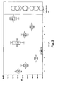
- Figure 2 is a graph showing the volume resistivity of various polymeric adhesive/additive mixtures as determined in the experiments reported in Example 1 below.
- Figure 3 is a graph plotting the average volume resistivities of the various mixtures shown in Figure 2 with additive concentration.
- Figure 4 is a graph similar to Figure 3 but showing the variation of the volume resistivities of polymeric adhesive/tetrabutylammonium hexafluorophosphate mixtures with salt concentration as determined in the experiments reported in Example 2 below.
- certain additives to control the volume resistivity of adhesive materials used, for example, in adhesive layers of electro-optic assemblies and displays, are disclosed herein.
- the adhesive layers disclosed herein enable the volume resistivity to be varied without substantially varying the mechanical properties of the adhesive layer.
- the adhesive layers through the addition of one or more additives, expand the selection of adhesive materials which have desirable mechanical properties but which could not otherwise be used because their volume resistivities are unsuitable.
- one can "fine tune" the volume resistivity of an adhesive layer i.e., to adjust the volume resistivity of the material to an optimum value for a particular display or electrophoretic medium.
- the electro-optic assembly of the present invention may constitute a complete electro-optic display or only a sub-assembly of such a display.
- a complete electro-optic display requires the presence of at least one, and normally two, electrodes to produce the electric field necessary to vary the optical state of the electro-optic material, although in some cases only one of the two electrodes may be a permanent part of the display, with the other electrode being in the form a movable stylus or similar instrument which can be moved over the display to write on the display.
- each of the first and second substrates will comprise at least one electrode.
- the assembly may have the form of an active matrix display, with the first substrate comprising a single continuous light-transmissive electrode extending across multiple pixels, and typically the whole, of the display (in practice, the first substrate normally also comprises a polymeric film or similar supporting layer which supports the relatively thin light-transmissive electrode and protects the relatively fragile electrode from mechanical damage), while the second substrate has the form of a backplane comprising a support portion and a plurality of pixel electrodes, which define the individual pixels of the display.
- such a backplane may further comprise non-linear devices (typically thin film transistors) and other circuitry used to produce on the pixel electrodes the potentials needed to drive the display (i.e., to switch the various pixels to the optical states necessary to provide a desired image on the display).
- non-linear devices typically thin film transistors
- other circuitry used to produce on the pixel electrodes the potentials needed to drive the display (i.e., to switch the various pixels to the optical states necessary to provide a desired image on the display).
- the electro-optic assembly of the present invention may constitute a sub-assembly of such a complete display.
- the electro-optic assembly may have the form of a front plane laminate as described in the aforementioned US 2004/0027327 .
- one of the substrates (for convenience, say the first substrate) comprises a light-transmissive electrically-conductive layer intended to form the front electrode of a final display (again, the first substrate will normally also comprise a polymeric film or similar supporting layer which supports the relatively thin electrically-conductive layer and protect it from mechanical damage), while the second substrate comprises a release sheet, which is removed before the front plane laminate is laminated to a backplane to form the final display.
- double release sheets of the present invention can be regarded as special types of electro-optic assemblies of the invention.
- double release sheets typically comprise a layer of electro-optic material having adhesive layers on both sides thereof, both adhesive layers being covered by release sheets.
- Such a double release sheet comprises an electro-optic assembly of the present invention in which both substrates are release sheets.
- the salt additive may be an inorganic salt, organic salt, or combination thereof.
- Exemplary salts include potassium acetate, and tetraalkylammonium salts, especially tetrabutylammonium salts such as the chloride.
- Further examples of salts include lithium salts such as LiCF 3 SOF 3 , LiCIO 4 , LiPF 6 , LiBF 4 , LiAsF 6 , and LiN(CF 3 SO 2 ) 3 .
- the presently preferred salt is tetrabutylammonium hexafluorophosphate, largely because of the stability and inertness of this salt.
- the polymeric adhesive material that is used in the adhesive layer can be any polymeric material that fulfills the particular needs of the end-use application.
- suitable polymeric adhesive materials include polyurethane, vinyl acetate, vinyl acetate ethylene, epoxy, a polyacrylic-based adhesive, or combinations thereof. These adhesive materials may be solvent based or aqueous based.
- An example of a particular polyurethane that can used is described in copending U. S. Application Serial No. 10/715,916 filed 18 November 2003 and assigned to Air Products and Chemicals, Inc.
- the additive incorporated into a polymeric adhesive material may be formed in situ ; in other words, one or more precursor materials may be incorporated into the polymeric adhesive material where the precursor material(s) can react with one another, or with the polymeric adhesive, or be changed by exposure of the adhesive material to conditions (for example, exposure to heat, light, or magnetic or electric fields) which cause a change in the precursor materials to form the final additive.
- the adhesive material may contain components other than the additive (or other dopant) used to adjust its volume resistivity; for example, the adhesive material may also contain a dye or other colorant.
- a color filter as a separate layer on the viewing surface of the display (the surface through which an observer views the display), this color filter containing pixels of differing colors, for example red, green and blue.
- this color filter containing pixels of differing colors, for example red, green and blue.
- an "optical biasing element” may be provided in the lamination adhesive of an encapsulated electrophoretic display to adjust the appearance of the display.
- the provision of such an optical biasing element may affect the electrical properties of the adhesive, and the electrical properties of an adhesive containing such an optical biasing element may be optimized by use of the additives described herein.
- the optimum amount of salt additive will of course vary widely with the exact adhesive material and the exact additive used, and the desired volume resistivity of the final mixture. However, by way of general guidance it may be indicated that a concentration of from about 10 -5 to about 10 -4 moles of additive per gram of adhesive has been found to give useful results. This range is for 1:1 salt additives such as tetrabutylammonium chloride, tetrabutylammonium hexafluorophosphate and potassium acetate; if 1:2 salts such as sodium carbonate or calcium chloride are used, lower concentrations, of the order of 10 -6 moles of salt per gram of adhesive may suffice. As shown in the Examples below, the volume resistivity of adhesive materials typically varies in a predictable manner with the concentration of the additive, and hence the final choice of how much additive should be added to achieve a desired volume resistivity may readily be determined empirically.
- salts have been added to polymers used as lamination adhesives in prior art electro-optic displays, for example as biocides to protect the polymers from biological degradation during extended storage, such salts are typically used up during storage as they perform their biocidal or similar function.
- the additives used in the present invention are intended to be permanent constituents of the lamination adhesive since they are intended to effect a permanent adjustment in the conductivity thereof.
- the optimum amounts of additives used are typically substantially greater than the amounts of salts used as biocides etc.
- the additive typically, no special procedures are required to incorporate the additive into the adhesive material. If, as is typically the case, the adhesive layer is formed by coating a film of a latex or solution of the adhesive material on to a substrate, or on to the electro-optic material, and drying to form the adhesive layer, the additive will normally simply be dissolved or dispersed in the latex or solution of the adhesive material before coating.
- the additive may be added to the latex or solution neat or may be dissolved in an aqueous solution, non-aqueous solution, or combination thereof.
- the choice of the specific additive to be used is governed largely by considerations of compatibility with the other components of the adhesive layer and solubility in the adhesive material to which the additive is to be added. If, as is typically the case, the additive is to be added to an aqueous latex of the adhesive material, the additive should be chosen to have good water solubility, so that among salts alkali metal and substituted ammonium salts are generally preferred. Care should be taken to ensure that the additive does not cause aggregation of the latex particles. Also, the additive should desirably not cause major changes in the pH of the adhesive material, and should not chemically react with the adhesive material or other parts of the final display with which it eventually comes into contact, for example the backplane.
- one or more salt additives greatly expands the range of polymeric materials, which can be used as lamination adhesives in electro-optic displays.
- the addition of one or more additives enables the use of polymeric materials which have mechanical properties highly desirable in electro-optic displays but which have volume resistivities in their pure states too high to be useful.
- the addition of the one or more additive may be used to replace water-based polyurethane dispersions hitherto used in such displays with non-hygroscopic and/or hydrophobic polymeric materials.
- modified adhesives disclosed herein may be useful in applications other than electro-optic displays.
- FIG. 1 is a schematic section through one such assembly having the form of a front plane laminate.
- This electro-optic assembly comprises a substrate, a conductive layer, an electro-optic layer, an adhesive layer, and a second substrate in the form of a release sheet; the assembly is illustrated at an intermediate stage of the manufacturing process for an electro-optic display before the subassembly is laminated to a second assembly, namely a backplane.
- the front plane laminate (generally designated 100) shown in Figure 1 comprises a light-transmissive substrate 110, a light-transmissive electrode layer 120, an electro-optic layer 130, a lamination adhesive layer 180 and a release sheet 190; the release sheet is illustrated in the process of being removed from the lamination adhesive layer 180 preparatory to lamination of the FPL 100 to a backplane.
- the substrate 110 is typically a transparent plastic films, such as a 7 mil (177 ⁇ m) polyethylene terephthalate sheet.
- the lower surface (in Figure 1 ) of substrate 110 which forms the viewing surface of the final display, may have one or more additional layers (not shown), for example a protective layer to absorb ultra-violet radiation, barrier layers to prevent ingress of oxygen or moisture into the final display, and anti-reflection coatings to improve the optical properties of the display.
- Coated onto the upper surface of substrate 110 is the thin light-transmissive electrically conductive layer 120, preferably of ITO, which acts as the common front electrode in the final display. PET films coated with ITO are available commercially
- the electro-optic layer 130 may be deposited on the conductive layer 120, typically by slot coating, the two layers being in electrical contact.
- the electro-optic layer 130 shown in Figure 1 is an encapsulated electrophoretic medium and comprises microcapsules 140, each of which comprises negatively charged white particles 150 and positively charged black particles 160 suspended in a hydrocarbon-based suspending fluid 165.
- the microcapsules 140 are held retained within a polymeric binder 170.
- white particles 150 move to the positive electrode and black particles 160 move to the negative electrode, so that electro-optic layer 130 appears, to an observer viewing the display through substrate 110, white or black depending on whether conductive layer 120 is positive or negative relative to the adjacent pixel electrode in the backplane.
- the FPL 100 is desirably prepared by coating the lamination adhesive 180, in liquid form, conveniently by slot coating, on to release sheet 190, drying (or otherwise curing) the adhesive to form a solid layer, and then laminating the adhesive and release sheet to the electro-optic layer 130, which has previously been coated on to the substrate 110 bearing the conductive layer 120; this lamination may conveniently be effected using hot roll lamination.
- the lamination adhesive may be applied over the electro-optic layer 130 and then dried or otherwise cured before being covered with the release sheet 190.
- the release sheet 190 is conveniently a 7 mil (177 ⁇ m) film; depending upon the nature of the electro-optic medium used, it may be desirable to coat this film with a release agent, for example a silicone. As illustrated in Figure 1 , the release sheet 190 is peeled or otherwise removed from the lamination adhesive 180 before the FPL 100 is laminated to a backplane (not shown) to form the final display.
- An additive for example tetrabutylammonium hexafluorophosphate, is included in the lamination adhesive 180.
- the additive is conveniently added to the liquid form of the lamination adhesive before coating to form the layer 180, as already described.
- a base adhesive material was prepared by blending NeoRez (Registered Trade Mark) 9630 and NeoRez 9330, two polyurethane dispersions available commercially from NeoResins, Inc., 730 Main Street, Wilmington MA 01887. This material was divided into eight samples of approximately 50 g each, each sample containing 40 per cent by weight of solids, and varying amounts of potassium acetate, tetrabutylammonium chloride, or poly(acrylic acid) aqueous solution were added as indicated in the Table below; a control sample was also provided with no additives.
- NeoRez Registered Trade Mark
- NeoRez 9330 two polyurethane dispersions available commercially from NeoResins, Inc., 730 Main Street, Wilmington MA 01887. This material was divided into eight samples of approximately 50 g each, each sample containing 40 per cent by weight of solids, and varying amounts of potassium acetate, tetrabutylammonium chloride, or poly(acrylic acid) aqueous solution were added
- each of the samples was mixed for a period of 7 to 10 days to ensure a thoroughly homogeneous product and to re-disperse any gel-like solids, which formed as a result of adding the additive as a solid to the sample.
- visual inspection confirmed that all the samples were free from any significant amount of gel.
- the salt-containing dispersions thus prepared were coated in the same way as in Example 1 above and dried at 60°C in air for at least 10 minutes to produce dried adhesive layers having thicknesses from 12 to 20 ⁇ m.
- the resultant adhesive layers were then converted to single pixel test units in the same way as in Example 1 above; at least three test units were used for each salt concentration.
- Control test units containing the same polyurethane adhesive without any additive were also prepared.
- the completed test units were conditioned at 30°C and 30 per cent relative humidity for one week prior to resistivity testing.
- volume resistivity of the test units was then measured using driving pulses of 15V and 300 msec duration, and the resultant data plotted in Figure 4 of the accompanying drawings. From this Figure it will be seen that the addition of the NBu 4 PF 6 resulted in a substantial decrease in the volume resistivity of the adhesive material, by about two orders of magnitude over the range of salt concentrations tested, and that the volume resistivity varied linearly with salt concentration.
Abstract
Description
- Electro-optic assemblies useful in the production of electro-optic displays, and to materials for use in such assemblies are disclosed. More specifically, adhesive compositions having controlled volume resistivity, and electro-optic assemblies incorporating such materials, are disclosed. The materials disclosed herein may be useful in applications other than electro-optic displays.
- Electro-optic displays comprise a layer of electro-optic material, a term which is used herein in its conventional meaning in the art to refer to a material having first and second display states differing in at least one optical property, the material being changed from its first to its second display state by application of an electric field to the material. The optical property is typically color perceptible to the human eye, but may be another optical property, such as optical transmission, reflectance, luminescence or, in the case of displays intended for machine reading, pseudo-color in the sense of a change in reflectance of electromagnetic wavelengths outside the visible range.
- The electro-optic assemblies of the present invention typically contain an electro-optic material, which is a solid in the sense that the electro-optic material has solid external surfaces, although the material may, and often does, have internal liquid- or gas-filled spaces, and to methods for assembling displays using such an electro-optic material. Displays using such solid electro-optic materials may hereinafter for convenience be referred to as "solid electro-optic displays". Thus, the term "solid electro-optic displays" includes rotating bichromal member displays (see below), encapsulated electrophoretic displays, microcell electrophoretic displays and encapsulated liquid crystal displays.
- The terms "bistable" and "bistability" are used herein in their conventional meaning in the art to refer to displays comprising display elements having first and second display states differing in at least one optical property, and such that after any given element has been driven, by means of an addressing pulse of finite duration, to assume either its first or second display state, after the addressing pulse has terminated, that state will persist for at least several times, for example at least four times, the minimum duration of the addressing pulse required to change the state of the display element. It is shown in published
U.S. Patent Application No. 2002/0180687 that some particle-based electrophoretic displays capable of gray scale are stable not only in their extreme black and white states but also in their intermediate gray states, and the same is true of some other types of electro-optic displays. This type of display is properly called "multi-stable" rather than bistable, although for convenience the term "bistable" may be used herein to cover both bistable and multi-stable displays. - Several types of electro-optic displays are known. One type of electro-optic display is a rotating bichromal member type as described, for example, in
U.S. Patents Nos. 5,808,783 ;5,777,782 ;5,760,761 ;6,054,071 6,055,091 ;6,097,531 ;6,128,124 ;6,137,467 ; and6,147,791 (although this type of display is often referred to as a "rotating bichromal ball" display, the term "rotating bichromal member" is preferred as more accurate since in some of the patents mentioned above the rotating members are not spherical). Such a display uses a large number of small bodies (typically spherical or cylindrical), which have two or more sections with differing optical characteristics, and an internal dipole. These bodies are suspended within liquid-filled vacuoles within a matrix, the vacuoles being filled with liquid so that the bodies are free to rotate. The appearance of the display is changed to applying an electric field thereto, thus rotating the bodies to various positions and varying which of the sections of the bodies is seen through a viewing surface. This type of electro-optic medium is typically bistable. - Another type of electro-optic display uses an electrochromic medium, for example an electrochromic medium in the form of a nanochromic film comprising an electrode formed at least in part from a semi-conducting metal oxide and a plurality of dye molecules capable of reversible color change attached to the electrode; see, for example O'Regan, B., et al., Nature 1991, 353, 737; and Wood, D., Information Display, 18(3), 24 (March 2002). See also Bach, U., et al., Adv. Mater., 2002, 14(11), 845. Nanochromic films of this type are also described, for example, in
U.S. Patent No. 6,301,038 , International Application Publication No.WO 01/27690 U.S. Patent Application 2003/0214695 . This type of medium is also typically bistable. - Another type of electro-optic display, which has been the subject of intense research and development for a number of years, is the particle-based electrophoretic display, in which a plurality of charged particles moves through a suspending fluid under the influence of an electric field. Electrophoretic displays can have attributes of good brightness and contrast, wide viewing angles, state bistability, and low power consumption when compared with liquid crystal displays. Nevertheless, problems with the long-term image quality of these displays have prevented their widespread usage. For example, particles that make up electrophoretic displays tend to settle, resulting in inadequate service-life for these displays.
- Numerous patents and applications assigned to or in the names of the Massachusetts Institute of Technology (MIT) and E Ink Corporation have recently been published describing encapsulated electrophoretic media. Such encapsulated media comprise numerous small capsules, each of which itself comprises an internal phase containing electrophoretically-mobile particles suspended in a liquid suspending medium, and a capsule wall surrounding the internal phase. Typically, the capsules are themselves held within a polymeric binder to form a coherent layer positioned between two electrodes. Encapsulated media of this type are described, for example, in
U.S. Patents Nos. 5,930,026 ;5,961,804 ;6,017,584 ;6,067,185 ;6,118,426 ;6,120,588 ;6,120,839 ;6,124,851 ;6,130,773 ;6,130,774 ;6,172,798 ;6,177,921 ;6,232,950 ;6,249,721 ;6,252,564 ;6,262,706 ;6,262,833 ;6,300,932 ;6,312,304 ;6,312,971 ;6,323,989 ;6,327,072 ;6,376,828 ;6,377,387 ;6,392,785 ;6,392,786 ;6,413,790 ;6,422,687 ;6,445,374 ;6,445,489 ;6,459,418 ;6,473,072 ;6,480,182 ;6,498,114 ;6,504,524 ;6,506,438 ;6,512,354 ;6,515,649 ;6,518,949 ;6,521,489 ;6,531,997 ;6,535,197 ;6,538,801 ;6,545,291 ;6,580,545 ;6,639,578 ;6,652,075 ;6,657,772 ;6,664,944 ;6,680,725 ;6,683,333 ; and6,704,133 ; andU.S. Patent Applications Publication Nos. 2002/0019081 ;2002/0021270 ;2002/0053900 ;2002/0060321 ;2002/0063661 ;2002/0063677 ;2002/0090980 ;2002/0106847 ;2002/0113770 ;2002/0130832 ;2002/0131147 ;2002/0145792 ;2002/0171910 ;2002/0180687 ;2002/0180688 ;2002/0185378 ;2003/0011560 ;2003/0011868 ;2003/0020844 ;2003/0025855 ;2003/0034949 ;2003/0038755 ;2003/0053189 ;2003/0096113 ;2003/0102858 ;2003/0132908 ;2003/0137521 ;2003/0137717 ;2003/0151702 ;2003/0189749 ;2003/0214695 ;2003/0214697 ;2003/0222315 ;2004/0008398 ;2004/0012839 ;2004/0014265 ; and2004/0027327 ; and International Applications Publication Nos.WO 99/67678 WO 00/05704WO 00/38000WO 00/38001WO00/36560 WO 00/67110WO 00/67327WO 01/07961 WO 01/08241 WO 03/092077 WO 03/107,315 - Many of the aforementioned patents and applications recognize that the walls surrounding the discrete microcapsules in an encapsulated electrophoretic medium could be replaced by a continuous phase, thus producing a so-called "polymer-dispersed electrophoretic display" in which the electrophoretic medium comprises a plurality of discrete droplets of an electrophoretic fluid and a continuous phase of a polymeric material, and that the discrete droplets of electrophoretic fluid within such a polymer-dispersed electrophoretic display may be regarded as capsules or microcapsules even though no discrete capsule membrane is associated with each individual droplet; see for example, the aforementioned
US 2002/0131147 . Accordingly, for purposes of the present application, such polymer-dispersed electrophoretic media are regarded as subspecies of encapsulated electrophoretic media. - An encapsulated electrophoretic display typically does not suffer from the clustering and settling failure mode of traditional electrophoretic devices and provides further advantages, such as the ability to print or coat the display on a wide variety of flexible and rigid substrates. (Use of the word "printing" is intended to include all forms of printing and coating, including, but without limitation: pre-metered coatings such as patch die coating, slot or extrusion coating, slide or cascade coating, curtain coating; roll coating such as knife over roll coating, forward and reverse roll coating; gravure coating; dip coating; spray coating; meniscus coating; spin coating; brush coating; air knife coating; silk screen printing processes; electrostatic printing processes; thermal printing processes; ink jet printing processes; and other similar techniques.) Thus, the resulting display can be flexible. Further, because the display medium can be printed (using a variety of methods), the display itself can be made inexpensively.
- A related type of electrophoretic display is a so-called "microcell electrophoretic display". In a microcell electrophoretic display, the charged particles and the suspending fluid are not encapsulated within capsules but instead are retained within a plurality of cavities formed within a carrier medium, typically a polymeric film. See, for example, International Application Publication No.
WO 02/01281 U.S. Patent Application Publication No. 2002/0075556 , both assigned to Sipix Imaging, Inc. - Other types of electro-optic materials, for example, polymer-dispersed liquid crystal, may also be used in the assemblies of the present invention.
- Although electrophoretic media are often opaque (since, for example, in many electrophoretic media, the particles substantially block transmission of visible light through the display) and operate in a reflective mode, many electrophoretic displays can be made to operate in a so-called "shutter mode" in which one display state is substantially opaque and one is light-transmissive. See, for example, the aforementioned
U.S. Patents Nos. 6,130,774 and6,172,798 , andU.S. Patents Nos. 5,872,552 ;6,144,361 ;6,271,823 ;6,225,971 ; and6,184,856 . Dielectrophoretic displays, which are similar to electrophoretic displays but rely upon variations in electric field strength, can operate in a similar mode; seeU.S. Patent No. 4,418,346 . - In addition to the layer of electro-optic material, an electro-optic display normally comprises at least two other layers disposed on opposed sides of the electro-optic material, one of these two layers being an electrode layer. In most such displays both the layers are electrode layers, and one or both of the electrode layers are patterned to defme the pixels of the display For example, one electrode layer may be patterned into elongate row electrodes and the other into elongate column electrodes running at right angles to the row electrodes, the pixels being defined by the intersections of the row and column electrodes. Alternatively, and more commonly, one electrode layer has the form of a single continuous electrode and the other electrode layer is patterned into a matrix of pixel electrodes, each of which defines one pixel of the display. In another type of electro-optic display, which is intended for use with a stylus, print head or similar movable electrode separate from the display, only one of the layers adjacent the electro-optic layer comprises an electrode, the layer on the opposed side of the electro-optic layer typically being a protective layer intended to prevent the movable electrode damaging the electro-optic layer.
- The manufacture of a three-layer electro-optic display normally involves at least one lamination operation. For example, in several of the aforementioned MIT and E Ink patents and applications, there is described a process for manufacturing an encapsulated electrophoretic display in which an encapsulated electrophoretic medium comprising capsules in a binder is coated on to a flexible substrate comprising indium-tin-oxide (ITO) or a similar conductive coating (which acts as an one electrode of the final display) on a plastic film, the capsules/binder coating being dried to form a coherent layer of the electrophoretic medium firmly adhered to the substrate. Separately, a backplane, containing an array of pixel electrodes and an appropriate arrangement of conductors to connect the pixel electrodes to drive circuitry, is prepared. To form the final display, the substrate having the capsule/binder layer thereon is laminated to the backplane using a lamination adhesive. (A very similar process can be used to prepare an electrophoretic display useable with a stylus or similar movable electrode by replacing the backplane with a simple protective layer, such as a plastic film, over which the stylus or other movable electrode can slide.) In one preferred form of such a process, the backplane is itself flexible and is prepared by printing the pixel electrodes and conductors on a plastic film or other flexible substrate. The obvious lamination technique for mass production of displays by this process is roll lamination using a lamination adhesive. Similar manufacturing techniques can be used with other types of electro-optic displays. For example, a microcell electrophoretic medium or a rotating bichromal member medium may be laminated to a backplane in substantially the same manner as an encapsulated electrophoretic medium.
- In the processes described above, the lamination of the substrate tarrying the electro-optic layer to the backplane may advantageously be carried out by vacuum lamination. Vacuum lamination is effective in expelling air from between the two materials being laminated, thus avoiding unwanted air bubbles in the final display; such air bubbles may introduce undesirable artifacts in the images produced on the display. However, vacuum lamination of the two parts of an electro-optic display in this manner imposes stringent requirements upon the lamination adhesive used, especially in the case of a display using an encapsulated electrophoretic medium. The lamination adhesive should have/sufficient adhesive strength to bind the electro-optic layer to the layer (typically an electrode layer) to which it is to be laminated, and in the case of an encapsulated electrophoretic medium, the adhesive should also have sufficient adhesive strength to mechanically hold the capsules together. If the electro-optic display is to be of a flexible type (and one of the important advantages of rotating bichromal member and encapsulated electrophoretic displays is that they can be made flexible), the adhesive should have sufficient flexibility not to introduce defects into the display when the display is flexed. The lamination adhesive should have adequate flow properties at the lamination temperature to ensure high quality lamination, and in this regard, the demands of laminating encapsulated electrophoretic and some other types of electro-optic media are unusually difficult; the lamination has be conducted at a temperature of not more than about 130°C since the medium cannot be exposed to substantially higher temperatures without damage, but the flow of the adhesive must cope with the relatively uneven surface of the capsule-containing layer, the surface of which is rendered irregular by the underlying capsules. The lamination temperature should indeed be kept as low as possible, and room temperature lamination would be ideal, but no commercial adhesive has been found which permits such room temperature lamination. The lamination adhesive should be chemically compatible with all the other materials in the display.
-
WO 03/007067 - Japanese Published Application No.
05-239233 - Japanese Published Application No.
07-113050 - Japanese Published Application No.
2002-212364 - Japanese Published Application No.
63-248859 - Japanese Published Application No.
2000-111935 -
U.S. Patent Application Publication No. 2003/0011560 describes an electrophoretic display element including an electrophoretic display medium, an optical biasing element to modify an optical characteristic of the electrophoretic display element, and an addressing electrode to address the electrophoretic display medium. -
WO 03/007066 - Japanese Published Application No.
58-002823 - European Patent Application No.
873,986 - Japanese Published Application No.
11-092727 - As discussed in detail in the aforementioned
US 2003/0025855 , a lamination adhesive used in an electro-optic display should meet certain electrical criteria, and this introduces considerable problems in the selection of the lamination adhesive. Commercial manufacturers of lamination adhesives naturally devote considerable effort to ensuring that properties, such as strength of adhesion and lamination temperatures, of such adhesives are adjusted so that the adhesives perform well in their major applications, which typically involve laminating polymeric and similar films. However, in such applications, the electrical properties of the lamination adhesive are not relevant, and consequently the commercial manufacturers pay no heed to such electrical properties. Indeed, substantial variations (of up to several fold) in certain electrical properties may exist between different batches of the same commercial lamination adhesive, presumably because the manufacturer was attempting to optimize non-electrical properties of the lamination adhesive (for example, resistance to bacterial growth) and was not at all concerned about resulting changes in electrical properties. - However, in electro-optic displays, in which the lamination adhesive is normally located between the electrodes, which apply the electric field needed to change the electrical state of the electro-optic medium, the electrical properties of the adhesive may become crucial. As will be apparent to electrical engineers, the volume resistivity of the lamination adhesive becomes important, since the voltage drop across the electro-optic medium is essentially equal to the voltage drop across the electrodes, minus the voltage drop across the lamination adhesive. If the resistivity of the adhesive layer is too high, a substantial voltage drop will occur within the adhesive layer, requiring an increase in voltage across the electrodes. Increasing the voltage across the electrodes in this manner is undesirable, since it increases the power consumption of the display, and may require the use of more complex and expensive control circuitry to handle the increased voltage involved. On the other hand, if the adhesive layer, which extends continuously across the display, is in contact with a matrix of electrodes, as in an active matrix display, the volume resistivity of the adhesive layer should not be too low, or lateral conduction of electric current through the continuous adhesive layer may cause undesirable cross-talk between adjacent electrodes. Also, since the volume resistivity of most materials decreases rapidly with increasing temperature, if the volume resistivity of the adhesive is too low, the performance of the display at temperatures substantially above room temperature is adversely affected. For these reasons, there is an optimum range of lamination adhesive resistivity values for use with any given electro-optic medium, this range varying with the resistivity of the electro-optic medium. The volume resistivities of encapsulated electrophoretic media are typically around 1010 ohm cm, and the resistivities of other electro-optic media are usually of the same order of magnitude. Accordingly, the volume resistivity of the lamination adhesive should normally be around 108 to 1012 ohm cm, or about 109 to 1011 ohm cm, at the operating temperature of the display, typically around 20°C. The lamination adhesive should also have a variation of volume resistivity with temperature which is similar to that of the electro-optic medium itself.
- The number of commercial materials which can meet most of the previously discussed, rather disparate requirements for a lamination adhesive for use in an electro-optic display is small, and in practice a small number of water-dispersed urethane emulsions have been used for this purpose. A similar group of materials have been used as the binder for an encapsulated electrophoretic medium.
- However, the use of such polyester-based urethane emulsions as lamination adhesives is still a not entirely satisfactory compromise between the desired mechanical and electrical properties. Lamination adhesives such as acrylic polymers and pressure sensitive adhesives are available with much better mechanical properties, but the electrical properties of these materials are unsuitable for use in electro-optic displays. Moreover, hitherto there has been no satisfactory way of varying the electrical properties of the urethane emulsions to "fine tune" them to match the electrical properties of a specific electro-optic medium. Accordingly, it would be highly advantageous if some way could be found to "decouple" the mechanical and electrical properties of a lamination adhesive so that each set of properties could be optimized separately.
- Furthermore, in considering the choice of a lamination adhesive for use in an electro-optic display, attention must be paid to the process by which the display is to be assembled. Most prior art methods for final lamination of electrophoretic displays are essentially batch methods in which the electro-optic medium, the lamination adhesive and the backplane are only brought together immediately prior to final assembly, and it is desirable to provide methods better adapted for mass production. However, the aforementioned
US 2004/0027327 describes a method of assembling a solid electro-optic display (including a particle-based electrophoretic display), which is well adapted for mass production. Essentially, this copending application describes a so-called "front plane laminate" ("FPL") which comprises, in order, a light-transmissive electrically-conductive layer; a layer of a solid electro-optic medium in electrical contact with the electrically-conductive layer; an adhesive layer; and a release sheet. Typically, the light-transmissive electrically-conductive layer will be carried on a light-transmissive substrate, which is preferably flexible, in the sense that the substrate can be manually wrapped around a drum (say) 10 inches (254 mm) in diameter without permanent deformation. The term "light-transmissive" is used in this copending application and herein to mean that the layer thus designated transmits sufficient light to enable an observer, looking through that layer, to observe the change in display states of the electro-optic medium, which will be normally be viewed through the electrically-conductive layer and adjacent substrate (if present). The substrate will be typically be a polymeric film, and will normally have a thickness in the range of about 1 to about 25 mil (25 to 634 µm), preferably about 2 to about 10 mil (51 to 254 µm). The electrically-conductive layer is conveniently a thin metal layer of, for example, aluminum or indium-tin-oxide, or may be a conductive polymer. Polyethylene terephthalate (PET) films coated with aluminum or ITO are available commercially, for example as "aluminized Mylar" ("Mylar" is a Registered Trade Mark) from E.I. du Pont de Nemours & Company, Wilmington DE, and such commercial materials may be used with good results in the front plane laminate. - Assembly of an electro-optic display using such a front plane laminate may be effected by removing the release sheet from the front plane laminate and contacting the adhesive layer with the backplane under conditions effective to cause the adhesive layer to adhere to the backplane, thereby securing the adhesive layer, electro-optic medium layer and electrically-conductive layer to the backplane. This process is well-adapted to mass production since the front plane laminate may be mass produced, typically using roll-to-roll coating techniques, and then cut into pieces of any size needed for use with specific backplanes.
- The aforementioned
US 2004/0027327 also describes a method four testing the electro-optic medium in a front plane laminate prior to incorporation of the front plane laminate into a display. In this testing method, the release sheet is provided with an electrically conductive layer, and a voltage sufficient to change the optical state of the electro-optic medium is applied between this electrically conductive layer and the electrically conductive layer on the opposed side of the electro-optic medium. Observation of the electro-optic medium will then reveal any faults in the medium, thus avoiding laminating faulty electro-optic medium into a display, with the resultant cost of scrapping the entire display, not merely the faulty front plane laminate. - The aforementioned
US 2004/0027327 also describes a second methods for testing the electro-optic medium in a front plane laminate by placing an electrostatic charge on the release sheet, thus forming an image on the electro-optic medium. This image is then observed in the same way as before to detect any faults in the electro-optic medium. - International Application No.
PCT/US03/27686 describes a so-called "double release film" which is essentially a simplified version of the front plane laminate previously described. One form of the double release sheet comprises a layer of a solid electro-optic medium sandwiched between two adhesive layers, one or both of the adhesive layers being covered by a release sheet. Another form of the double release sheet comprises a layer of a solid electro-optic medium sandwiched between two release sheets. Both forms of the double release film are intended for use in a process generally similar to the process for assembling an electro-optic display from a front plane laminate already described, but involving two separate laminations; typically, in a first lamination the double release sheet is laminated to a front electrode to form a front sub-assembly, and then in a second lamination the front sub-assembly is laminated to a backplane to form the final display. - In view of the advantages of the assembly method using a front plane laminate described in the aforementioned
US 2004/0027327 , it is desirable that lamination adhesive be capable of being incorporated into such a front plane laminate. It is also desirable that a lamination adhesive be capable of being incorporated into a double release film as previously described. - Accordingly, in one aspect there is provided an electro-optic assembly comprising first and second substrates, and an adhesive layer and a layer of electro-optic material disposed between the first and second substrates, the adhesive layer comprising a mixture of a polymeric adhesive material and a salt, the adhesive layer comprising from about 10-6 to about 10-4 moles of additive per gram of the polymeric adhesive material. Typically, the layer will comprise from about 10-5 to about 10-4 moles of additive per gram of polymeric adhesive material. The layer may comprise a polyurethane, vinyl acetate, vinyl acetate ethylene, epoxy, or a polyacrylic based adhesive.
- The salt used in the electro-optic assembly of the present invention may be, for example, an inorganic salt, an organic salt, or a combination thereof. In one particular embodiment, the salt comprises potassium acetate. In an alternative embodiment, the salt may comprise a quaternary ammonium salt, for example a tetraalkylammonium salt, such as tetrabutylammonium chloride or hexafluorophosphate.
- The adhesive layer containing the additive may provide other functions besides an adhesive function. For example, the layer may be provided with regions of differing colors and serve as a color filter. Alternatively, the layer may comprise an optical biasing element.
- In the electro-optic assembly, at least one of the first and second substrates may comprise an electrode. In one particular embodiment, each of the first and second substrates comprises at least one electrode. In another particular embodiment, the first substrate may comprise a light-transmissive electrically-conductive layer (which can act as an electrode), the second substrate may comprise a release sheet, and the electro-optic medium may be a solid electro-optic medium; thus, the entire electro-optic assembly will have the form of a front plane laminate as described in the aforementioned
US 2004/0027327 . - In a further aspect of the present invention, there is provided an article of manufacture (a double release sheet) comprising: a layer of a solid electro-optic medium having first and second surfaces on opposed sides thereof; a first adhesive layer on the first surface of the layer of solid electro-optic medium; a release sheet disposed on the opposed side of the first adhesive layer from the layer of solid electro-optic medium; and a second adhesive layer on the second surface of the layer of solid electro-optic medium, at least one of the first and second adhesive layers comprising a mixture of a polymeric adhesive material and a salt, the at least one adhesive layer comprising from 10-6 to 10-4 moles of salt per gram of polymeric adhesive material.
-
Figure 1 is a schematic cross-section through an electro-optic assembly of the present invention having the form of a front plane laminate. -
Figure 2 is a graph showing the volume resistivity of various polymeric adhesive/additive mixtures as determined in the experiments reported in Example 1 below. -
Figure 3 is a graph plotting the average volume resistivities of the various mixtures shown inFigure 2 with additive concentration. -
Figure 4 is a graph similar toFigure 3 but showing the variation of the volume resistivities of polymeric adhesive/tetrabutylammonium hexafluorophosphate mixtures with salt concentration as determined in the experiments reported in Example 2 below. - As already indicated, certain additives to control the volume resistivity of adhesive materials used, for example, in adhesive layers of electro-optic assemblies and displays, are disclosed herein. The adhesive layers disclosed herein enable the volume resistivity to be varied without substantially varying the mechanical properties of the adhesive layer. The adhesive layers, through the addition of one or more additives, expand the selection of adhesive materials which have desirable mechanical properties but which could not otherwise be used because their volume resistivities are unsuitable. Thus, one can "fine tune" the volume resistivity of an adhesive layer, i.e., to adjust the volume resistivity of the material to an optimum value for a particular display or electrophoretic medium.
- The electro-optic assembly of the present invention may constitute a complete electro-optic display or only a sub-assembly of such a display. As already indicated, and as discussed at length in the aforementioned E Ink and MIT patents and applications, a complete electro-optic display requires the presence of at least one, and normally two, electrodes to produce the electric field necessary to vary the optical state of the electro-optic material, although in some cases only one of the two electrodes may be a permanent part of the display, with the other electrode being in the form a movable stylus or similar instrument which can be moved over the display to write on the display. When the electro-optic assembly of the present invention is in the form of a complete display with two or more permanent electrodes, each of the first and second substrates will comprise at least one electrode. For example, the assembly may have the form of an active matrix display, with the first substrate comprising a single continuous light-transmissive electrode extending across multiple pixels, and typically the whole, of the display (in practice, the first substrate normally also comprises a polymeric film or similar supporting layer which supports the relatively thin light-transmissive electrode and protects the relatively fragile electrode from mechanical damage), while the second substrate has the form of a backplane comprising a support portion and a plurality of pixel electrodes, which define the individual pixels of the display. Obviously, such a backplane may further comprise non-linear devices (typically thin film transistors) and other circuitry used to produce on the pixel electrodes the potentials needed to drive the display (i.e., to switch the various pixels to the optical states necessary to provide a desired image on the display).
- Alternatively, the electro-optic assembly of the present invention may constitute a sub-assembly of such a complete display. In particular, the electro-optic assembly may have the form of a front plane laminate as described in the aforementioned
US 2004/0027327 . In such a front plane laminate, one of the substrates (for convenience, say the first substrate) comprises a light-transmissive electrically-conductive layer intended to form the front electrode of a final display (again, the first substrate will normally also comprise a polymeric film or similar supporting layer which supports the relatively thin electrically-conductive layer and protect it from mechanical damage), while the second substrate comprises a release sheet, which is removed before the front plane laminate is laminated to a backplane to form the final display. - Indeed, many of the double release sheets of the present invention can be regarded as special types of electro-optic assemblies of the invention. In practice, such double release sheets typically comprise a layer of electro-optic material having adhesive layers on both sides thereof, both adhesive layers being covered by release sheets. Such a double release sheet comprises an electro-optic assembly of the present invention in which both substrates are release sheets.
- In certain embodiments, the salt additive may be an inorganic salt, organic salt, or combination thereof. Exemplary salts include potassium acetate, and tetraalkylammonium salts, especially tetrabutylammonium salts such as the chloride. Further examples of salts include lithium salts such as LiCF3SOF3, LiCIO4, LiPF6, LiBF4, LiAsF6, and LiN(CF3SO2)3. The presently preferred salt is tetrabutylammonium hexafluorophosphate, largely because of the stability and inertness of this salt.
- The polymeric adhesive material that is used in the adhesive layer can be any polymeric material that fulfills the particular needs of the end-use application. Examples of suitable polymeric adhesive materials include polyurethane, vinyl acetate, vinyl acetate ethylene, epoxy, a polyacrylic-based adhesive, or combinations thereof. These adhesive materials may be solvent based or aqueous based. An example of a particular polyurethane that can used is described in copending
U. S. Application Serial No. 10/715,916 filed 18 November 2003 - The additive incorporated into a polymeric adhesive material may be formed in situ; in other words, one or more precursor materials may be incorporated into the polymeric adhesive material where the precursor material(s) can react with one another, or with the polymeric adhesive, or be changed by exposure of the adhesive material to conditions (for example, exposure to heat, light, or magnetic or electric fields) which cause a change in the precursor materials to form the final additive.
- The adhesive material may contain components other than the additive (or other dopant) used to adjust its volume resistivity; for example, the adhesive material may also contain a dye or other colorant. It is known to form full color electro-optic displays by providing a color filter as a separate layer on the viewing surface of the display (the surface through which an observer views the display), this color filter containing pixels of differing colors, for example red, green and blue. However, when a color filter is spaced from the electro-optic material in this manner, there is the possibility of image distortion when the color image is viewed at a substantial angle to the perpendicular to the viewing surface. To avoid such problems, it is in principle desirable to place the color filter immediately adjacent the electro-optic material itself. However, this requires placing the color filter between the electrodes of the display, so that the electrical properties of the color filter will affect the performance of the display. This is a particular problem with a color filter, since such filters are usually formed by dying a polymeric base material with three differing dyes, or mixtures of dyes, to form the red, green and blue or other colored portions, and it is unlikely that the three differing dyes will affect the electrical properties of the color filter in the same manner. The adhesive layers described herein may be used to counteract the effects of the differing dyes and render the electrical properties of the color filter substantially uniform, thereby avoiding artifacts on the image due to non-uniform electrical properties within the color filter.
- It is also known (see the aforementioned
US 2003/0011560 ) that an "optical biasing element" may be provided in the lamination adhesive of an encapsulated electrophoretic display to adjust the appearance of the display. The provision of such an optical biasing element may affect the electrical properties of the adhesive, and the electrical properties of an adhesive containing such an optical biasing element may be optimized by use of the additives described herein. - The optimum amount of salt additive will of course vary widely with the exact adhesive material and the exact additive used, and the desired volume resistivity of the final mixture. However, by way of general guidance it may be indicated that a concentration of from about 10-5 to about 10-4 moles of additive per gram of adhesive has been found to give useful results. This range is for 1:1 salt additives such as tetrabutylammonium chloride, tetrabutylammonium hexafluorophosphate and potassium acetate; if 1:2 salts such as sodium carbonate or calcium chloride are used, lower concentrations, of the order of 10-6 moles of salt per gram of adhesive may suffice. As shown in the Examples below, the volume resistivity of adhesive materials typically varies in a predictable manner with the concentration of the additive, and hence the final choice of how much additive should be added to achieve a desired volume resistivity may readily be determined empirically.
- Although small amounts of salts have been added to polymers used as lamination adhesives in prior art electro-optic displays, for example as biocides to protect the polymers from biological degradation during extended storage, such salts are typically used up during storage as they perform their biocidal or similar function. In contrast, the additives used in the present invention are intended to be permanent constituents of the lamination adhesive since they are intended to effect a permanent adjustment in the conductivity thereof. Also, the optimum amounts of additives used are typically substantially greater than the amounts of salts used as biocides etc.
- Typically, no special procedures are required to incorporate the additive into the adhesive material. If, as is typically the case, the adhesive layer is formed by coating a film of a latex or solution of the adhesive material on to a substrate, or on to the electro-optic material, and drying to form the adhesive layer, the additive will normally simply be dissolved or dispersed in the latex or solution of the adhesive material before coating. The additive may be added to the latex or solution neat or may be dissolved in an aqueous solution, non-aqueous solution, or combination thereof. It is of course necessary to ensure that the additive is uniformly dispersed throughout the adhesive material in order to prevent variations in conductivity within the final adhesive layer, but those skilled in coating technology will be familiar with routine techniques, such as lengthy agitation on a roll mill, for ensuring such uniform dispersion.
- The choice of the specific additive to be used is governed largely by considerations of compatibility with the other components of the adhesive layer and solubility in the adhesive material to which the additive is to be added. If, as is typically the case, the additive is to be added to an aqueous latex of the adhesive material, the additive should be chosen to have good water solubility, so that among salts alkali metal and substituted ammonium salts are generally preferred. Care should be taken to ensure that the additive does not cause aggregation of the latex particles. Also, the additive should desirably not cause major changes in the pH of the adhesive material, and should not chemically react with the adhesive material or other parts of the final display with which it eventually comes into contact, for example the backplane.
- The addition of one or more salt additives greatly expands the range of polymeric materials, which can be used as lamination adhesives in electro-optic displays. In particular, the addition of one or more additives enables the use of polymeric materials which have mechanical properties highly desirable in electro-optic displays but which have volume resistivities in their pure states too high to be useful. Also, since some electro-optic displays, especially encapsulated electrophoretic displays and electrochromic displays, are sensitive to moisture, the addition of the one or more additive may be used to replace water-based polyurethane dispersions hitherto used in such displays with non-hygroscopic and/or hydrophobic polymeric materials.
- It will be appreciated that the modified adhesives disclosed herein may be useful in applications other than electro-optic displays.
- A particularly preferred embodiment of the electro-optic assembly of the present invention will now be described, though by way of illustration only, with reference to
Figure 1 of the accompanying drawings, which is a schematic section through one such assembly having the form of a front plane laminate. This electro-optic assembly comprises a substrate, a conductive layer, an electro-optic layer, an adhesive layer, and a second substrate in the form of a release sheet; the assembly is illustrated at an intermediate stage of the manufacturing process for an electro-optic display before the subassembly is laminated to a second assembly, namely a backplane. - The front plane laminate (generally designated 100) shown in
Figure 1 comprises a light-transmissive substrate 110, a light-transmissive electrode layer 120, an electro-optic layer 130, alamination adhesive layer 180 and arelease sheet 190; the release sheet is illustrated in the process of being removed from thelamination adhesive layer 180 preparatory to lamination of theFPL 100 to a backplane. - The
substrate 110 is typically a transparent plastic films, such as a 7 mil (177 µm) polyethylene terephthalate sheet. The lower surface (inFigure 1 ) ofsubstrate 110, which forms the viewing surface of the final display, may have one or more additional layers (not shown), for example a protective layer to absorb ultra-violet radiation, barrier layers to prevent ingress of oxygen or moisture into the final display, and anti-reflection coatings to improve the optical properties of the display. Coated onto the upper surface ofsubstrate 110 is the thin light-transmissive electricallyconductive layer 120, preferably of ITO, which acts as the common front electrode in the final display. PET films coated with ITO are available commercially - The electro-
optic layer 130 may be deposited on theconductive layer 120, typically by slot coating, the two layers being in electrical contact. The electro-optic layer 130 shown inFigure 1 is an encapsulated electrophoretic medium and comprisesmicrocapsules 140, each of which comprises negatively chargedwhite particles 150 and positively chargedblack particles 160 suspended in a hydrocarbon-based suspending fluid 165. Themicrocapsules 140 are held retained within apolymeric binder 170. Upon application of an electrical field across electro-optic layer 130,white particles 150 move to the positive electrode andblack particles 160 move to the negative electrode, so that electro-optic layer 130 appears, to an observer viewing the display throughsubstrate 110, white or black depending on whetherconductive layer 120 is positive or negative relative to the adjacent pixel electrode in the backplane. - The
FPL 100 is desirably prepared by coating thelamination adhesive 180, in liquid form, conveniently by slot coating, on to releasesheet 190, drying (or otherwise curing) the adhesive to form a solid layer, and then laminating the adhesive and release sheet to the electro-optic layer 130, which has previously been coated on to thesubstrate 110 bearing theconductive layer 120; this lamination may conveniently be effected using hot roll lamination. (Alternatively, but less desirably, the lamination adhesive may be applied over the electro-optic layer 130 and then dried or otherwise cured before being covered with therelease sheet 190.) Therelease sheet 190 is conveniently a 7 mil (177 µm) film; depending upon the nature of the electro-optic medium used, it may be desirable to coat this film with a release agent, for example a silicone. As illustrated inFigure 1 , therelease sheet 190 is peeled or otherwise removed from thelamination adhesive 180 before theFPL 100 is laminated to a backplane (not shown) to form the final display. - An additive, for example tetrabutylammonium hexafluorophosphate, is included in the
lamination adhesive 180. The additive is conveniently added to the liquid form of the lamination adhesive before coating to form thelayer 180, as already described. - The following Examples are now given, though by way of illustration only, to show details of preferred materials, conditions and techniques used in the present invention.
- A base adhesive material was prepared by blending NeoRez (Registered Trade Mark) 9630 and NeoRez 9330, two polyurethane dispersions available commercially from NeoResins, Inc., 730 Main Street, Wilmington MA 01887. This material was divided into eight samples of approximately 50 g each, each sample containing 40 per cent by weight of solids, and varying amounts of potassium acetate, tetrabutylammonium chloride, or poly(acrylic acid) aqueous solution were added as indicated in the Table below; a control sample was also provided with no additives.
-
Table Sample No. Weight of sample (g) Additive Mass (g) of additive 0 50.12 N/ A 0 1 50.00 Bu4NCl 0.012 2 50.06 Bu4NCl 0.051 3 50.30 Bu4NCl 0.099 4 50.10 KOAc 0.007 5 49.99 KOAc 0.040 6 50.00 KOAc 0.082 7 50.00 PAA, sodium salt (40% wt aq.) 0.156 - Each of the samples was mixed for a period of 7 to 10 days to ensure a thoroughly homogeneous product and to re-disperse any gel-like solids, which formed as a result of adding the additive as a solid to the sample. At the end of each mixing period, visual inspection confirmed that all the samples were free from any significant amount of gel.
- Each sample was then coated on to a release sheet and dried to produce a layer of adhesive approximately 40 µm thick. The dried film was laminated to the conductive surface of a poly(ethylene terephthalate) film provided with an indium tin oxide coating, the release sheet was removed and the exposed surface of the adhesive laminated to an experimental 2 inch by 2 inch (51 by 51 mm) backplane comprising a polymeric film coated with a layer of graphite to produce a single-pixel test unit (essentially a single-pixel display minus the layer of electro-optic medium). The resultant test units were conditioned for 5 days at 25°C and 30 per cent relative humidity. The thickness of the adhesive was measured and recorded, and the resistance of the adhesive layer was determined. The volume resistivity of the adhesive was then determined from these measurements and the results are shown in
Figure 2 of the accompanying drawings.Figure 3 shows the average results fromFigure 2 against the additive concentration. - From the results in
Figures 2 and3 it will be seen that the additives altered the volume resistivity of the adhesive by about an order of magnitude, and that the variation in volume resistivity was reasonably linear with additive concentration. - Example 2
- This Example illustrates the effect of tetrabutylammonium hexafluorophosphate (NBu4PF6) in lowering the volume resistivity of an adhesive material as described in the aforementioned copending Application Serial No. 10/715,916.
- Stock solutions of NBu4FF6 containing from 10 to 200 mg of the salt per gram of solution were prepared, and added to various aliquots of a polyurethane dispersion to produce the desired levels of the salt ranging from 10-7 to 10-4 moles of the salt per gram of adhesive solids (approximately 100 to 100,000 ppm of the salt on a weight/weight adhesive solids basis). The resultant salt solution/dispersion mixtures were mixed on a roller mill for at least three hours to ensure complete mixing.
- The salt-containing dispersions thus prepared were coated in the same way as in Example 1 above and dried at 60°C in air for at least 10 minutes to produce dried adhesive layers having thicknesses from 12 to 20 µm. The resultant adhesive layers were then converted to single pixel test units in the same way as in Example 1 above; at least three test units were used for each salt concentration. Control test units containing the same polyurethane adhesive without any additive were also prepared. The completed test units were conditioned at 30°C and 30 per cent relative humidity for one week prior to resistivity testing.
- The volume resistivity of the test units was then measured using driving pulses of 15V and 300 msec duration, and the resultant data plotted in
Figure 4 of the accompanying drawings. From this Figure it will be seen that the addition of the NBu4PF6 resulted in a substantial decrease in the volume resistivity of the adhesive material, by about two orders of magnitude over the range of salt concentrations tested, and that the volume resistivity varied linearly with salt concentration.
Claims (13)
- An electro-optic assembly (100) comprising first (110) and second (190) substrates, and an adhesive layer (180) and a layer of electro-optic material (130) disposed between the first and second substrates (110, 190), wherein the adhesive layer (180) comprises a mixture of a polymeric adhesive material and a salt, characterized in that the adhesive layer (180) comprises from 10-6 to 10-4 moles of salt per gram of polymeric adhesive material.
- An electro-optic assembly according to claim 1 wherein the salt comprises potassium acetate.
- An electro-optic assembly according to claim 1 wherein the salt comprises a quaternary ammonium salt.
- An electro-optic assembly according to claim 3 wherein the salt comprises a tetraalkylammonium salt.
- An electro-optic assembly according to claim 4 wherein the salt comprises tetrabutylammonium chloride or hexafluorophosphate.
- An electro-optic assembly according to claim 1 wherein the adhesive layer (180) is provided with regions of differing colors and serves as a color filter.
- An electro-optic assembly according to claim 1 wherein the adhesive layer (180) further comprises an optical biasing element.
- An electro-optic assembly according to claim 1 wherein the adhesive layer (180) comprises from 10-5 to 10-4 moles of salt per gram of polymeric adhesive material.
- An electro-optic assembly according to claim 1 wherein the adhesive layer (180) comprises a polyurethane.
- An electro-optic assembly according to claim 1 wherein at least one of the first and second substrates (110, 190) comprises an electrode (120).
- An electro-optic assembly according to claim 10 wherein each of the first and second substrates (110, 190) comprises at least one electrode.
- An electro-optic assembly according to claim 10 wherein the first substrate (110) comprises a light-transmissive electrically-conductive electrode (120), the second substrate (190) comprises a release sheet, and the electro-optic medium (130) is a solid electro-optic medium.
- An article of manufacture comprising:a layer of a solid electro-optic medium having first and second surfaces on opposed sides thereof;a first adhesive layer on the first surface of the layer of solid electro-optic medium;a release sheet disposed on the opposed side of the first adhesive layer from the layer of solid electro-optic medium; anda second adhesive layer on the second surface of the layer of solid electro-optic medium,wherein at least one of the first and second adhesive layers comprises a mixture of a polymeric adhesive material and a salt, characterized in that the at least one adhesive layer (180) comprises from 10-6 to 10-4 moles of salt per gram of polymeric adhesive material.
Priority Applications (1)
| Application Number | Priority Date | Filing Date | Title |
|---|---|---|---|
| EP10010394A EP2273307B1 (en) | 2003-03-27 | 2004-03-26 | Electrophoretic medium for an electrophoretic display |
Applications Claiming Priority (2)
| Application Number | Priority Date | Filing Date | Title |
|---|---|---|---|
| US32005903P | 2003-03-27 | 2003-03-27 | |
| PCT/US2004/009198 WO2004088395A2 (en) | 2003-03-27 | 2004-03-26 | Electro-optic assemblies |
Related Child Applications (1)
| Application Number | Title | Priority Date | Filing Date |
|---|---|---|---|
| EP10010394A Division EP2273307B1 (en) | 2003-03-27 | 2004-03-26 | Electrophoretic medium for an electrophoretic display |
Publications (3)
| Publication Number | Publication Date |
|---|---|
| EP1616217A2 EP1616217A2 (en) | 2006-01-18 |
| EP1616217A4 EP1616217A4 (en) | 2007-04-11 |
| EP1616217B1 true EP1616217B1 (en) | 2010-10-20 |
Family
ID=33130237
Family Applications (2)
| Application Number | Title | Priority Date | Filing Date |
|---|---|---|---|
| EP10010394A Expired - Lifetime EP2273307B1 (en) | 2003-03-27 | 2004-03-26 | Electrophoretic medium for an electrophoretic display |
| EP04758361A Expired - Lifetime EP1616217B1 (en) | 2003-03-27 | 2004-03-26 | Electro-optic assemblies |
Family Applications Before (1)
| Application Number | Title | Priority Date | Filing Date |
|---|---|---|---|
| EP10010394A Expired - Lifetime EP2273307B1 (en) | 2003-03-27 | 2004-03-26 | Electrophoretic medium for an electrophoretic display |
Country Status (8)
| Country | Link |
|---|---|
| US (2) | US7012735B2 (en) |
| EP (2) | EP2273307B1 (en) |
| JP (2) | JP5044215B2 (en) |
| CN (1) | CN100399109C (en) |
| AT (1) | ATE485535T1 (en) |
| DE (1) | DE602004029661D1 (en) |
| HK (1) | HK1088075A1 (en) |
| WO (1) | WO2004088395A2 (en) |
Cited By (1)
| Publication number | Priority date | Publication date | Assignee | Title |
|---|---|---|---|---|
| TWI755081B (en) * | 2020-09-30 | 2022-02-11 | 美商電子墨水股份有限公司 | Electro-optic display and composite materials having low thermal sensitivity for use therein |
Families Citing this family (222)
| Publication number | Priority date | Publication date | Assignee | Title |
|---|---|---|---|---|
| US7193625B2 (en) * | 1999-04-30 | 2007-03-20 | E Ink Corporation | Methods for driving electro-optic displays, and apparatus for use therein |
| US7327511B2 (en) * | 2004-03-23 | 2008-02-05 | E Ink Corporation | Light modulators |
| US7999787B2 (en) * | 1995-07-20 | 2011-08-16 | E Ink Corporation | Methods for driving electrophoretic displays using dielectrophoretic forces |
| US7411719B2 (en) | 1995-07-20 | 2008-08-12 | E Ink Corporation | Electrophoretic medium and process for the production thereof |
| US8139050B2 (en) * | 1995-07-20 | 2012-03-20 | E Ink Corporation | Addressing schemes for electronic displays |
| US7848006B2 (en) * | 1995-07-20 | 2010-12-07 | E Ink Corporation | Electrophoretic displays with controlled amounts of pigment |
| US7583251B2 (en) * | 1995-07-20 | 2009-09-01 | E Ink Corporation | Dielectrophoretic displays |
| US8040594B2 (en) | 1997-08-28 | 2011-10-18 | E Ink Corporation | Multi-color electrophoretic displays |
| EP1093600B1 (en) | 1998-07-08 | 2004-09-15 | E Ink Corporation | Methods for achieving improved color in microencapsulated electrophoretic devices |
| US7119772B2 (en) * | 1999-04-30 | 2006-10-10 | E Ink Corporation | Methods for driving bistable electro-optic displays, and apparatus for use therein |
| US8009348B2 (en) * | 1999-05-03 | 2011-08-30 | E Ink Corporation | Machine-readable displays |
| US7119759B2 (en) * | 1999-05-03 | 2006-10-10 | E Ink Corporation | Machine-readable displays |
| US8115729B2 (en) | 1999-05-03 | 2012-02-14 | E Ink Corporation | Electrophoretic display element with filler particles |
| US7893435B2 (en) * | 2000-04-18 | 2011-02-22 | E Ink Corporation | Flexible electronic circuits and displays including a backplane comprising a patterned metal foil having a plurality of apertures extending therethrough |
| AU2002250304A1 (en) * | 2001-03-13 | 2002-09-24 | E Ink Corporation | Apparatus for displaying drawings |
| US8390918B2 (en) * | 2001-04-02 | 2013-03-05 | E Ink Corporation | Electrophoretic displays with controlled amounts of pigment |
| US20050156340A1 (en) | 2004-01-20 | 2005-07-21 | E Ink Corporation | Preparation of capsules |
| US7230750B2 (en) * | 2001-05-15 | 2007-06-12 | E Ink Corporation | Electrophoretic media and processes for the production thereof |
| US7679814B2 (en) | 2001-04-02 | 2010-03-16 | E Ink Corporation | Materials for use in electrophoretic displays |
| US8582196B2 (en) | 2001-05-15 | 2013-11-12 | E Ink Corporation | Electrophoretic particles and processes for the production thereof |
| US6982178B2 (en) * | 2002-06-10 | 2006-01-03 | E Ink Corporation | Components and methods for use in electro-optic displays |
| US7535624B2 (en) * | 2001-07-09 | 2009-05-19 | E Ink Corporation | Electro-optic display and materials for use therein |
| US7528822B2 (en) * | 2001-11-20 | 2009-05-05 | E Ink Corporation | Methods for driving electro-optic displays |
| US8558783B2 (en) | 2001-11-20 | 2013-10-15 | E Ink Corporation | Electro-optic displays with reduced remnant voltage |
| US9530363B2 (en) | 2001-11-20 | 2016-12-27 | E Ink Corporation | Methods and apparatus for driving electro-optic displays |
| US8593396B2 (en) | 2001-11-20 | 2013-11-26 | E Ink Corporation | Methods and apparatus for driving electro-optic displays |
| US9412314B2 (en) | 2001-11-20 | 2016-08-09 | E Ink Corporation | Methods for driving electro-optic displays |
| US8125501B2 (en) | 2001-11-20 | 2012-02-28 | E Ink Corporation | Voltage modulated driver circuits for electro-optic displays |
| US7952557B2 (en) * | 2001-11-20 | 2011-05-31 | E Ink Corporation | Methods and apparatus for driving electro-optic displays |
| US7190008B2 (en) | 2002-04-24 | 2007-03-13 | E Ink Corporation | Electro-optic displays, and components for use therein |
| US7223672B2 (en) * | 2002-04-24 | 2007-05-29 | E Ink Corporation | Processes for forming backplanes for electro-optic displays |
| US8049947B2 (en) * | 2002-06-10 | 2011-11-01 | E Ink Corporation | Components and methods for use in electro-optic displays |
| US8363299B2 (en) * | 2002-06-10 | 2013-01-29 | E Ink Corporation | Electro-optic displays, and processes for the production thereof |
| US7583427B2 (en) * | 2002-06-10 | 2009-09-01 | E Ink Corporation | Components and methods for use in electro-optic displays |
| US7649674B2 (en) * | 2002-06-10 | 2010-01-19 | E Ink Corporation | Electro-optic display with edge seal |
| US7843621B2 (en) * | 2002-06-10 | 2010-11-30 | E Ink Corporation | Components and testing methods for use in the production of electro-optic displays |
| US7110164B2 (en) * | 2002-06-10 | 2006-09-19 | E Ink Corporation | Electro-optic displays, and processes for the production thereof |
| US9470950B2 (en) | 2002-06-10 | 2016-10-18 | E Ink Corporation | Electro-optic displays, and processes for the production thereof |
| US7554712B2 (en) * | 2005-06-23 | 2009-06-30 | E Ink Corporation | Edge seals for, and processes for assembly of, electro-optic displays |
| US20110199671A1 (en) * | 2002-06-13 | 2011-08-18 | E Ink Corporation | Methods for driving electrophoretic displays using dielectrophoretic forces |
| US20080024482A1 (en) | 2002-06-13 | 2008-01-31 | E Ink Corporation | Methods for driving electro-optic displays |
| US20060255322A1 (en) * | 2002-07-17 | 2006-11-16 | Wu Zarng-Arh G | Methods and compositions for improved electrophoretic display performance |
| TWI314237B (en) * | 2002-07-17 | 2009-09-01 | Sipix Imaging Inc | Novel methods and compositions for improved electrophoretic display performance |
| US7347957B2 (en) | 2003-07-10 | 2008-03-25 | Sipix Imaging, Inc. | Methods and compositions for improved electrophoretic display performance |
| US8547628B2 (en) | 2002-07-17 | 2013-10-01 | Sipix Imaging, Inc. | Methods and compositions for improved electrophoretic display performance |
| US7839564B2 (en) * | 2002-09-03 | 2010-11-23 | E Ink Corporation | Components and methods for use in electro-optic displays |
| EP3056941B1 (en) | 2002-09-03 | 2019-01-09 | E Ink Corporation | Electro-phoretic medium |
| US20130063333A1 (en) | 2002-10-16 | 2013-03-14 | E Ink Corporation | Electrophoretic displays |
| US7910175B2 (en) * | 2003-03-25 | 2011-03-22 | E Ink Corporation | Processes for the production of electrophoretic displays |
| WO2004088395A2 (en) * | 2003-03-27 | 2004-10-14 | E Ink Corporation | Electro-optic assemblies |
| US10726798B2 (en) | 2003-03-31 | 2020-07-28 | E Ink Corporation | Methods for operating electro-optic displays |
| WO2004099862A2 (en) * | 2003-05-02 | 2004-11-18 | E Ink Corporation | Electrophoretic displays |
| US8174490B2 (en) * | 2003-06-30 | 2012-05-08 | E Ink Corporation | Methods for driving electrophoretic displays |
| WO2005010598A2 (en) * | 2003-07-24 | 2005-02-03 | E Ink Corporation | Electro-optic displays |
| JP4806634B2 (en) * | 2003-08-19 | 2011-11-02 | イー インク コーポレイション | Electro-optic display and method for operating an electro-optic display |
| WO2005029458A1 (en) * | 2003-09-19 | 2005-03-31 | E Ink Corporation | Methods for reducing edge effects in electro-optic displays |
| DE602004016017D1 (en) * | 2003-10-08 | 2008-10-02 | E Ink Corp | ELECTRO-wetting DISPLAYS |
| US8319759B2 (en) | 2003-10-08 | 2012-11-27 | E Ink Corporation | Electrowetting displays |
| US7672040B2 (en) * | 2003-11-05 | 2010-03-02 | E Ink Corporation | Electro-optic displays, and materials for use therein |
| US8177942B2 (en) | 2003-11-05 | 2012-05-15 | E Ink Corporation | Electro-optic displays, and materials for use therein |
| US20110164301A1 (en) | 2003-11-05 | 2011-07-07 | E Ink Corporation | Electro-optic displays, and materials for use therein |
| US7551346B2 (en) * | 2003-11-05 | 2009-06-23 | E Ink Corporation | Electro-optic displays, and materials for use therein |
| JP5337344B2 (en) * | 2003-11-05 | 2013-11-06 | イー インク コーポレイション | Electro-optic display |
| US8928562B2 (en) | 2003-11-25 | 2015-01-06 | E Ink Corporation | Electro-optic displays, and methods for driving same |
| JP4790622B2 (en) | 2003-11-26 | 2011-10-12 | イー インク コーポレイション | Low residual voltage electro-optic display |
| US7206119B2 (en) * | 2003-12-31 | 2007-04-17 | E Ink Corporation | Electro-optic displays, and method for driving same |
| US7075703B2 (en) * | 2004-01-16 | 2006-07-11 | E Ink Corporation | Process for sealing electro-optic displays |
| US7504050B2 (en) * | 2004-02-23 | 2009-03-17 | Sipix Imaging, Inc. | Modification of electrical properties of display cells for improving electrophoretic display performance |
| US7388572B2 (en) * | 2004-02-27 | 2008-06-17 | E Ink Corporation | Backplanes for electro-optic displays |
| US7492339B2 (en) * | 2004-03-26 | 2009-02-17 | E Ink Corporation | Methods for driving bistable electro-optic displays |
| US8289250B2 (en) * | 2004-03-31 | 2012-10-16 | E Ink Corporation | Methods for driving electro-optic displays |
| US20050253777A1 (en) * | 2004-05-12 | 2005-11-17 | E Ink Corporation | Tiled displays and methods for driving same |
| US20080136774A1 (en) | 2004-07-27 | 2008-06-12 | E Ink Corporation | Methods for driving electrophoretic displays using dielectrophoretic forces |
| WO2006015044A1 (en) * | 2004-07-27 | 2006-02-09 | E Ink Corporation | Electro-optic displays |
| US11250794B2 (en) | 2004-07-27 | 2022-02-15 | E Ink Corporation | Methods for driving electrophoretic displays using dielectrophoretic forces |
| JP2006119495A (en) * | 2004-10-25 | 2006-05-11 | Toppan Printing Co Ltd | Electronic display |
| JP4644472B2 (en) * | 2004-11-16 | 2011-03-02 | セイコーエプソン株式会社 | Manufacturing method of display device |
| JP2008521065A (en) * | 2005-01-26 | 2008-06-19 | イー インク コーポレイション | Electrophoretic display using gaseous fluid |
| JP2006235013A (en) * | 2005-02-23 | 2006-09-07 | Seiko Epson Corp | Electrophoretic device, and electronic appliance |
| KR100980187B1 (en) * | 2005-06-07 | 2010-09-03 | 주식회사 엘지화학 | Polarizing plate |
| US20080043318A1 (en) * | 2005-10-18 | 2008-02-21 | E Ink Corporation | Color electro-optic displays, and processes for the production thereof |
| EP1938299A4 (en) * | 2005-10-18 | 2010-11-24 | E Ink Corp | Components for electro-optic displays |
| US20070091417A1 (en) * | 2005-10-25 | 2007-04-26 | E Ink Corporation | Electrophoretic media and displays with improved binder |
| JP5231730B2 (en) * | 2005-12-08 | 2013-07-10 | 小林クリエイト株式会社 | Information display medium |
| US20070186289A1 (en) * | 2006-02-03 | 2007-08-09 | Karp Nelson M | Animal model for HIV induced disease |
| US8173519B2 (en) * | 2006-03-03 | 2012-05-08 | Semiconductor Energy Laboratory Co., Ltd. | Method for manufacturing semiconductor device |
| US7733554B2 (en) | 2006-03-08 | 2010-06-08 | E Ink Corporation | Electro-optic displays, and materials and methods for production thereof |
| US7843624B2 (en) * | 2006-03-08 | 2010-11-30 | E Ink Corporation | Electro-optic displays, and materials and methods for production thereof |
| US8390301B2 (en) * | 2006-03-08 | 2013-03-05 | E Ink Corporation | Electro-optic displays, and materials and methods for production thereof |
| US8610988B2 (en) | 2006-03-09 | 2013-12-17 | E Ink Corporation | Electro-optic display with edge seal |
| US7952790B2 (en) | 2006-03-22 | 2011-05-31 | E Ink Corporation | Electro-optic media produced using ink jet printing |
| WO2007121104A2 (en) * | 2006-04-10 | 2007-10-25 | E Ink Corporation | Electro-optic displays, and materials for use therein |
| US7903319B2 (en) * | 2006-07-11 | 2011-03-08 | E Ink Corporation | Electrophoretic medium and display with improved image stability |
| US8018640B2 (en) * | 2006-07-13 | 2011-09-13 | E Ink Corporation | Particles for use in electrophoretic displays |
| US20080024429A1 (en) * | 2006-07-25 | 2008-01-31 | E Ink Corporation | Electrophoretic displays using gaseous fluids |
| US7492497B2 (en) * | 2006-08-02 | 2009-02-17 | E Ink Corporation | Multi-layer light modulator |
| WO2008036519A2 (en) * | 2006-09-18 | 2008-03-27 | E Ink Corporation | Color electro-optic displays |
| US7986450B2 (en) | 2006-09-22 | 2011-07-26 | E Ink Corporation | Electro-optic display and materials for use therein |
| US7477444B2 (en) * | 2006-09-22 | 2009-01-13 | E Ink Corporation & Air Products And Chemical, Inc. | Electro-optic display and materials for use therein |
| US7649666B2 (en) * | 2006-12-07 | 2010-01-19 | E Ink Corporation | Components and methods for use in electro-optic displays |
| US7688497B2 (en) * | 2007-01-22 | 2010-03-30 | E Ink Corporation | Multi-layer sheet for use in electro-optic displays |
| WO2008091850A2 (en) | 2007-01-22 | 2008-07-31 | E Ink Corporation | Multi-layer sheet for use in electro-optic displays |
| JP4297170B2 (en) * | 2007-02-23 | 2009-07-15 | セイコーエプソン株式会社 | Electrophoretic display sheet, electrophoretic display device, electrophoretic display device manufacturing method, and electronic apparatus |
| US7826129B2 (en) | 2007-03-06 | 2010-11-02 | E Ink Corporation | Materials for use in electrophoretic displays |
| KR20090130211A (en) * | 2007-05-21 | 2009-12-18 | 이 잉크 코포레이션 | Methods for driving video electro-optic displays |
| US9199441B2 (en) * | 2007-06-28 | 2015-12-01 | E Ink Corporation | Processes for the production of electro-optic displays, and color filters for use therein |
| WO2009006248A1 (en) | 2007-06-29 | 2009-01-08 | E Ink Corporation | Electro-optic displays, and materials and methods for production thereof |
| US8902153B2 (en) | 2007-08-03 | 2014-12-02 | E Ink Corporation | Electro-optic displays, and processes for their production |
| US20090122389A1 (en) * | 2007-11-14 | 2009-05-14 | E Ink Corporation | Electro-optic assemblies, and adhesives and binders for use therein |
| JP2011517490A (en) * | 2008-03-21 | 2011-06-09 | イー インク コーポレイション | Electro-optic display and color filter |
| WO2009126957A1 (en) | 2008-04-11 | 2009-10-15 | E Ink Corporation | Methods for driving electro-optic displays |
| US9782949B2 (en) | 2008-05-30 | 2017-10-10 | Corning Incorporated | Glass laminated articles and layered articles |
| WO2010021275A1 (en) | 2008-08-19 | 2010-02-25 | 日立化成工業株式会社 | Light-modulating film |
| EP2322986B1 (en) | 2008-08-19 | 2019-06-26 | Hitachi Chemical Company, Ltd. | Light-modulating film |
| JP2010102293A (en) * | 2008-09-26 | 2010-05-06 | Toppan Printing Co Ltd | Microcapsule-type electrophoretic display panel and method of manufacturing the same |
| US8457013B2 (en) | 2009-01-13 | 2013-06-04 | Metrologic Instruments, Inc. | Wireless dual-function network device dynamically switching and reconfiguring from a wireless network router state of operation into a wireless network coordinator state of operation in a wireless communication network |
| US20100177076A1 (en) * | 2009-01-13 | 2010-07-15 | Metrologic Instruments, Inc. | Edge-lit electronic-ink display device for use in indoor and outdoor environments |
| US8234507B2 (en) | 2009-01-13 | 2012-07-31 | Metrologic Instruments, Inc. | Electronic-ink display device employing a power switching mechanism automatically responsive to predefined states of device configuration |
| US20100177750A1 (en) * | 2009-01-13 | 2010-07-15 | Metrologic Instruments, Inc. | Wireless Diplay sensor communication network |
| TWI484273B (en) * | 2009-02-09 | 2015-05-11 | E Ink Corp | Electrophoretic particles |
| WO2010092954A1 (en) * | 2009-02-13 | 2010-08-19 | 日立化成工業株式会社 | Light modulation film |
| JP5749021B2 (en) | 2009-02-13 | 2015-07-15 | 日立化成株式会社 | Light control film |
| US8098418B2 (en) | 2009-03-03 | 2012-01-17 | E. Ink Corporation | Electro-optic displays, and color filters for use therein |
| US20100270055A1 (en) * | 2009-04-27 | 2010-10-28 | Air Products And Chemicals, Inc. | Electrically Conductive Films Formed From Dispersions Comprising Conductive Polymers and Polyurethanes |
| CA2770386A1 (en) * | 2009-08-07 | 2011-02-10 | Methode Electronics, Inc. | Assembly and method for illuminating through a circuit board |
| JP5859447B2 (en) | 2009-10-28 | 2016-02-10 | イー インク コーポレイション | Electro-optic display with touch sensor |
| US8654436B1 (en) | 2009-10-30 | 2014-02-18 | E Ink Corporation | Particles for use in electrophoretic displays |
| WO2011123847A2 (en) | 2010-04-02 | 2011-10-06 | E Ink Corporation | Electrophoretic media |
| JP5459030B2 (en) | 2010-04-08 | 2014-04-02 | セイコーエプソン株式会社 | Electrophoretic display device |
| CN105654889B (en) | 2010-04-09 | 2022-01-11 | 伊英克公司 | Method for driving electro-optic display |
| TWI484275B (en) | 2010-05-21 | 2015-05-11 | E Ink Corp | Electro-optic display, method for driving the same and microcavity electrophoretic display |
| JP5660853B2 (en) * | 2010-11-05 | 2015-01-28 | 三菱鉛筆株式会社 | Electrophoretic display medium sheet and electrophoretic display medium using the same |
| JP2011085948A (en) * | 2010-12-09 | 2011-04-28 | Seiko Epson Corp | Electrophoretic device and electronic equipment |
| JP5664412B2 (en) * | 2011-03-30 | 2015-02-04 | 凸版印刷株式会社 | Front plate of microcapsule type electrophoretic display device and microcapsule type electrophoretic display device |
| CN102253502A (en) * | 2011-04-18 | 2011-11-23 | 广州奥翼电子科技有限公司 | Bonding agent and electro-optic assembly and electrophoretic medium thereof |
| JP2013025066A (en) * | 2011-07-21 | 2013-02-04 | Seiko Epson Corp | Electro-optic device and electronic equipment |
| KR101271470B1 (en) * | 2011-08-08 | 2013-06-05 | 도레이첨단소재 주식회사 | Dielectric adhesive film for flexible display device with electronic paper |
| US20130125910A1 (en) | 2011-11-18 | 2013-05-23 | Avon Products, Inc. | Use of Electrophoretic Microcapsules in a Cosmetic Composition |
| JP5919967B2 (en) | 2012-04-02 | 2016-05-18 | セイコーエプソン株式会社 | Electrophoretic display device and electronic apparatus |
| KR101373833B1 (en) * | 2012-04-19 | 2014-03-14 | 도레이첨단소재 주식회사 | Dielectric adhesive film for flexible display device with electronic paper |
| US11467466B2 (en) | 2012-04-20 | 2022-10-11 | E Ink Corporation | Illumination systems for reflective displays |
| US10190743B2 (en) | 2012-04-20 | 2019-01-29 | E Ink Corporation | Illumination systems for reflective displays |
| KR101771740B1 (en) * | 2012-11-13 | 2017-08-25 | 삼성전기주식회사 | Thin film type chip device and method for manufacturing the same |
| CN103265897B (en) * | 2012-12-26 | 2015-03-25 | 上海中航光电子有限公司 | Optical bonding member and touch display device |
| US9715155B1 (en) | 2013-01-10 | 2017-07-25 | E Ink Corporation | Electrode structures for electro-optic displays |
| US9726957B2 (en) | 2013-01-10 | 2017-08-08 | E Ink Corporation | Electro-optic display with controlled electrochemical reactions |
| KR101856834B1 (en) | 2013-05-14 | 2018-05-10 | 이 잉크 코포레이션 | Colored electrophoretic displays |
| WO2015059029A1 (en) | 2013-10-22 | 2015-04-30 | Vlyte Innovations Limited | A wide operating temperature range electrophoretic device |
| CN103708412B (en) * | 2013-10-29 | 2016-01-20 | 太原科技大学 | A kind of micro electro-mechanical system packaging method |
| CN105917265B (en) * | 2014-01-17 | 2019-01-15 | 伊英克公司 | Electro-optic displays with two-phase electrode layer |
| JP6260309B2 (en) * | 2014-01-31 | 2018-01-17 | セイコーエプソン株式会社 | Display device |
| US10317767B2 (en) | 2014-02-07 | 2019-06-11 | E Ink Corporation | Electro-optic display backplane structure with drive components and pixel electrodes on opposed surfaces |
| US9671635B2 (en) | 2014-02-07 | 2017-06-06 | E Ink Corporation | Electro-optic display backplane structures with drive components and pixel electrodes on opposed surfaces |
| KR20150097359A (en) * | 2014-02-18 | 2015-08-26 | 주식회사 엘지화학 | Encapsulation film and organic electronic device comprising the same |
| US10446585B2 (en) | 2014-03-17 | 2019-10-15 | E Ink Corporation | Multi-layer expanding electrode structures for backplane assemblies |
| TWI613498B (en) * | 2014-06-27 | 2018-02-01 | 電子墨水加利福尼亞有限責任公司 | Anisotropic conductive dielectric layer for electrophoretic display |
| US10657869B2 (en) | 2014-09-10 | 2020-05-19 | E Ink Corporation | Methods for driving color electrophoretic displays |
| KR101824723B1 (en) | 2014-09-10 | 2018-02-02 | 이 잉크 코포레이션 | Colored electrophoretic displays |
| US9759978B2 (en) | 2014-10-17 | 2017-09-12 | E Ink California, Llc | Composition and process for sealing microcells |
| CA2963561A1 (en) | 2014-11-07 | 2016-05-12 | E Ink Corporation | Applications of electro-optic displays |
| US10197883B2 (en) | 2015-01-05 | 2019-02-05 | E Ink Corporation | Electro-optic displays, and methods for driving same |
| CN107111201B (en) | 2015-01-05 | 2021-01-29 | 伊英克公司 | Electro-optic display and method for driving an electro-optic display |
| US9835925B1 (en) | 2015-01-08 | 2017-12-05 | E Ink Corporation | Electro-optic displays, and processes for the production thereof |
| WO2016126771A1 (en) | 2015-02-04 | 2016-08-11 | E Ink Corporation | Electro-optic displays with reduced remnant voltage, and related apparatus and methods |
| US10997930B2 (en) | 2015-05-27 | 2021-05-04 | E Ink Corporation | Methods and circuitry for driving display devices |
| CN107771369B (en) | 2015-06-29 | 2021-09-24 | 伊英克公司 | Method for mechanically and electrically connecting to display electrodes |
| JP2018523727A (en) | 2015-07-23 | 2018-08-23 | イー インク コーポレイション | Polymer formulation for use with electro-optic media |
| CN113004854B (en) | 2015-09-30 | 2022-09-30 | 伊英克公司 | Polyurethane adhesive layer for electro-optical assemblies |
| PT3374435T (en) | 2015-11-11 | 2021-01-08 | E Ink Corp | Functionalized quinacridone pigments |
| EP3465339A4 (en) | 2016-05-31 | 2019-04-17 | E Ink Corporation | Backplanes for electro-optic displays |
| WO2018020333A1 (en) | 2016-07-29 | 2018-02-01 | Semiconductor Energy Laboratory Co., Ltd. | Separation method, display device, display module, and electronic device |
| TWI753868B (en) | 2016-08-05 | 2022-02-01 | 日商半導體能源研究所股份有限公司 | Peeling method, display device, display module and electronic device |
| TWI730017B (en) | 2016-08-09 | 2021-06-11 | 日商半導體能源研究所股份有限公司 | Manufacturing method of display device, display device, display module and electronic device |
| KR102425705B1 (en) | 2016-08-31 | 2022-07-28 | 가부시키가이샤 한도오따이 에네루기 켄큐쇼 | Method of manufacturing a semiconductor device |
| JP6981812B2 (en) | 2016-08-31 | 2021-12-17 | 株式会社半導体エネルギー研究所 | Manufacturing method of semiconductor device |
| US10369664B2 (en) | 2016-09-23 | 2019-08-06 | Semiconductor Energy Laboratory Co., Ltd. | Manufacturing method of semiconductor device |
| US10503041B2 (en) | 2016-11-30 | 2019-12-10 | E Ink Corporation | Laminated electro-optic displays and methods of making same |
| WO2018160546A1 (en) | 2017-02-28 | 2018-09-07 | E Ink Corporation | Writeable electrophoretic displays including sensing circuits and styli configured to interact with sensing circuits |
| TWI670556B (en) | 2017-03-28 | 2019-09-01 | 美商電子墨水股份有限公司 | Backplane for electro-optic display |
| CN106883808B (en) * | 2017-04-01 | 2021-02-12 | 广州奥翼电子科技股份有限公司 | Adhesive, preparation method thereof and electrophoretic display |
| US10495941B2 (en) | 2017-05-19 | 2019-12-03 | E Ink Corporation | Foldable electro-optic display including digitization and touch sensing |
| US11404013B2 (en) | 2017-05-30 | 2022-08-02 | E Ink Corporation | Electro-optic displays with resistors for discharging remnant charges |
| JP2020522741A (en) | 2017-05-30 | 2020-07-30 | イー インク コーポレイション | Electro-optic display |
| US10962816B2 (en) | 2017-06-16 | 2021-03-30 | E Ink Corporation | Flexible color-changing fibers and fabrics |
| EP4086318A3 (en) | 2017-06-16 | 2023-01-18 | E Ink Corporation | Variable transmission electrophoretic devices |
| WO2018232099A1 (en) | 2017-06-16 | 2018-12-20 | E Ink Corporation | Electro-optic media including encapsulated pigments in gelatin binder |
| EP3697535B1 (en) | 2017-10-18 | 2023-04-26 | Nuclera Nucleics Ltd | Digital microfluidic devices including dual substrates with thin-film transistors and capacitive sensing |
| US10824042B1 (en) | 2017-10-27 | 2020-11-03 | E Ink Corporation | Electro-optic display and composite materials having low thermal sensitivity for use therein |
| KR20210151997A (en) | 2017-11-03 | 2021-12-14 | 이 잉크 코포레이션 | Processes for producing electro-optic displays |
| JP2021507293A (en) | 2017-12-19 | 2021-02-22 | イー インク コーポレイション | Application of electro-optical display |
| PL3729191T3 (en) | 2017-12-22 | 2023-10-09 | E Ink Corporation | Electro-optic displays, and methods for driving same |
| WO2019160841A1 (en) | 2018-02-15 | 2019-08-22 | E Ink Corporation | Via placement for slim border electro-optic display backplanes with decreased capacitive coupling between t-wires and pixel electrodes |
| US11175561B1 (en) | 2018-04-12 | 2021-11-16 | E Ink Corporation | Electrophoretic display media with network electrodes and methods of making and using the same |
| CN109143718A (en) * | 2018-08-08 | 2019-01-04 | 广州奥翼电子科技股份有限公司 | A kind of high definition electrophoresis type display |
| US11353759B2 (en) | 2018-09-17 | 2022-06-07 | Nuclera Nucleics Ltd. | Backplanes with hexagonal and triangular electrodes |
| US11635640B2 (en) | 2018-10-01 | 2023-04-25 | E Ink Corporation | Switching fibers for textiles |
| US11656525B2 (en) | 2018-10-01 | 2023-05-23 | E Ink Corporation | Electro-optic fiber and methods of making the same |
| US11511096B2 (en) | 2018-10-15 | 2022-11-29 | E Ink Corporation | Digital microfluidic delivery device |
| KR102576895B1 (en) | 2018-11-09 | 2023-09-08 | 이 잉크 코포레이션 | Electro-optical displays |
| US11754903B1 (en) | 2018-11-16 | 2023-09-12 | E Ink Corporation | Electro-optic assemblies and materials for use therein |
| US11402719B2 (en) | 2018-12-11 | 2022-08-02 | E Ink Corporation | Retroreflective electro-optic displays |
| WO2020122917A1 (en) | 2018-12-13 | 2020-06-18 | E Ink Corporation | Illumination systems for reflective displays |
| US10823373B2 (en) | 2018-12-17 | 2020-11-03 | E Ink Corporation | Light emitting device including variable transmission film to control intensity and pattern |
| US11521565B2 (en) | 2018-12-28 | 2022-12-06 | E Ink Corporation | Crosstalk reduction for electro-optic displays |
| JP7201816B2 (en) | 2018-12-30 | 2023-01-10 | イー インク カリフォルニア, エルエルシー | electro-optic display |
| US11460722B2 (en) | 2019-05-10 | 2022-10-04 | E Ink Corporation | Colored electrophoretic displays |
| US11761123B2 (en) | 2019-08-07 | 2023-09-19 | E Ink Corporation | Switching ribbons for textiles |
| GB201914105D0 (en) | 2019-09-30 | 2019-11-13 | Vlyte Innovations Ltd | A see-through electrophoretic device having a visible grid |
| US11827816B2 (en) | 2019-10-07 | 2023-11-28 | E Ink Corporation | Adhesive composition comprising a polyurethane and a cationic dopant |
| CN114641723A (en) | 2019-11-14 | 2022-06-17 | 伊英克公司 | Electro-optic medium comprising oppositely charged particles and variable transmission device comprising the same |
| CA3163699A1 (en) | 2020-02-07 | 2021-08-12 | E Ink Corporation | Electrophoretic display layer with thin film top electrode |
| EP4162318A1 (en) | 2020-06-03 | 2023-04-12 | E Ink Corporation | Foldable electrophoretic display module including non-conductive support plate |
| US11846863B2 (en) | 2020-09-15 | 2023-12-19 | E Ink Corporation | Coordinated top electrode—drive electrode voltages for switching optical state of electrophoretic displays using positive and negative voltages of different magnitudes |
| EP4214573A1 (en) | 2020-09-15 | 2023-07-26 | E Ink Corporation | Improved driving voltages for advanced color electrophoretic displays and displays with improved driving voltages |
| JP2023541843A (en) | 2020-09-15 | 2023-10-04 | イー インク コーポレイション | Four-particle electrophoretic medium provides fast, high-contrast optical state switching |
| TW202314665A (en) | 2021-08-18 | 2023-04-01 | 美商電子墨水股份有限公司 | Methods for driving electro-optic displays |
| CN113717596B (en) * | 2021-08-18 | 2022-10-25 | 深圳秋田微电子股份有限公司 | Electrophoretic display coating liquid, preparation method thereof and electrophoretic display assembly |
| WO2023164078A1 (en) | 2022-02-25 | 2023-08-31 | E Ink Corporation | Electro-optic displays with edge seal components and methods of making the same |
| US11830449B2 (en) | 2022-03-01 | 2023-11-28 | E Ink Corporation | Electro-optic displays |
| WO2023211699A1 (en) | 2022-04-27 | 2023-11-02 | E Ink Corporation | Electro-optic display stacks with segmented electrodes and methods of making the same |
| CN117518667A (en) * | 2022-08-04 | 2024-02-06 | 广州奥翼电子科技股份有限公司 | Double stripping sheet and manufacturing method and application thereof |
| WO2024026951A1 (en) * | 2022-08-04 | 2024-02-08 | 广州奥翼电子科技股份有限公司 | Electro-optical material and manufacturing method therefor |
Citations (1)
| Publication number | Priority date | Publication date | Assignee | Title |
|---|---|---|---|---|
| JP2000212535A (en) * | 1996-01-18 | 2000-08-02 | Sanyo Chem Ind Ltd | Antistatic pressure-sensitive adhesive |
Family Cites Families (167)
| Publication number | Priority date | Publication date | Assignee | Title |
|---|---|---|---|---|
| US35941A (en) * | 1862-07-22 | Improvement in breech-loading fire-arms | ||
| US226820A (en) * | 1880-04-20 | ferguson | ||
| US257635A (en) * | 1882-05-09 | Extension-pipe for | ||
| US813A (en) * | 1838-06-30 | robinson | ||
| US112525A (en) * | 1871-03-14 | Improvement in dry-docks | ||
| US105036A (en) * | 1870-07-05 | Improved steam-packing | ||
| US75634A (en) * | 1868-03-17 | Improved composition foe roofing | ||
| US252360A (en) * | 1882-01-17 | Bread and meat slicer | ||
| US136048A (en) * | 1873-02-18 | Improvement in game-boards | ||
| US216837A (en) * | 1879-06-24 | Improvement in dies for making axle-boxes | ||
| US112750A (en) * | 1871-03-14 | Improvement in harvesters | ||
| US27635A (en) * | 1860-03-27 | Improvement in seeding-machines | ||
| US3540008A (en) * | 1967-12-20 | 1970-11-10 | Xerox Corp | Solid state storage devices having non-corona extinction capability |
| NL7005615A (en) | 1969-04-23 | 1970-10-27 | ||
| US3870517A (en) | 1969-10-18 | 1975-03-11 | Matsushita Electric Ind Co Ltd | Color image reproduction sheet employed in photoelectrophoretic imaging |
| US3668106A (en) | 1970-04-09 | 1972-06-06 | Matsushita Electric Ind Co Ltd | Electrophoretic display device |
| US3767392A (en) | 1970-04-15 | 1973-10-23 | Matsushita Electric Ind Co Ltd | Electrophoretic light image reproduction process |
| US3792308A (en) | 1970-06-08 | 1974-02-12 | Matsushita Electric Ind Co Ltd | Electrophoretic display device of the luminescent type |
| JPS4917079B1 (en) | 1970-12-21 | 1974-04-26 | ||
| US4448493A (en) | 1981-02-25 | 1984-05-15 | Toppan Printing Co., Ltd. | Electrochromic display device |
| US4418346A (en) | 1981-05-20 | 1983-11-29 | Batchelder J Samuel | Method and apparatus for providing a dielectrophoretic display of visual information |
| JPS582823A (en) * | 1981-06-29 | 1983-01-08 | Tomoegawa Paper Co Ltd | Color liquid-crystal display body |
| US4550982A (en) | 1981-11-09 | 1985-11-05 | Nippon Electric Co., Ltd. | All-solid-state display including an organic electrochromic layer with ion donor/acceptor |
| JPS63248859A (en) * | 1987-04-03 | 1988-10-17 | Mitsubishi Heavy Ind Ltd | Antistatic plastic material |
| FR2646966B1 (en) * | 1989-05-10 | 1996-02-02 | Elf Aquitaine | METHOD OF QUICK AND UNIFORM HEATING OF A MULTI-LAYER ASSEMBLY COMPRISING AT LEAST ONE THIN LAYER BASED ON A MACROMOLECULAR MATERIAL WITH INTERCALLED ION CONDUCTION BETWEEN TWO STRUCTURES WITH HIGH ELECTRON CONDUCTION |
| JPH05161618A (en) * | 1991-12-10 | 1993-06-29 | Terumo Corp | Conductive tacky adhesive for medical purpose |
| JPH0683267A (en) * | 1991-12-12 | 1994-03-25 | Honshu Paper Co Ltd | Antistatic adhesive label |
| JPH05239233A (en) * | 1992-02-28 | 1993-09-17 | Nippon Ester Co Ltd | Polyester film |
| JP3018906B2 (en) * | 1993-07-19 | 2000-03-13 | 株式会社ブリヂストン | Semiconductive polymer elastic member |
| US5378405A (en) * | 1993-07-28 | 1995-01-03 | Minnesota Mining And Manufacturing Company | Conductive microparticles and pressure-sensitive adhesive tapes made therefrom |
| JPH10502677A (en) | 1994-06-29 | 1998-03-10 | ローベルト ボツシユ ゲゼルシヤフト ミツト ベシユレンクテル ハフツング | Anisotropic conductive adhesive and method for producing anisotropic conductive adhesive |
| US5745094A (en) | 1994-12-28 | 1998-04-28 | International Business Machines Corporation | Electrophoretic display |
| US6137467A (en) | 1995-01-03 | 2000-10-24 | Xerox Corporation | Optically sensitive electric paper |
| US5784190A (en) | 1995-04-27 | 1998-07-21 | John M. Baker | Electro-micro-mechanical shutters on transparent substrates |
| US6111051A (en) | 1998-08-07 | 2000-08-29 | Mearthane Products Corporation | Preparation of conductive polyurethanes using a conductive quasi-solution |
| US7106296B1 (en) | 1995-07-20 | 2006-09-12 | E Ink Corporation | Electronic book with multiple page displays |
| US6120839A (en) | 1995-07-20 | 2000-09-19 | E Ink Corporation | Electro-osmotic displays and materials for making the same |
| US6124851A (en) | 1995-07-20 | 2000-09-26 | E Ink Corporation | Electronic book with multiple page displays |
| US6515649B1 (en) | 1995-07-20 | 2003-02-04 | E Ink Corporation | Suspended particle displays and materials for making the same |
| US6710540B1 (en) | 1995-07-20 | 2004-03-23 | E Ink Corporation | Electrostatically-addressable electrophoretic display |
| US6120588A (en) | 1996-07-19 | 2000-09-19 | E Ink Corporation | Electronically addressable microencapsulated ink and display thereof |
| US6727881B1 (en) | 1995-07-20 | 2004-04-27 | E Ink Corporation | Encapsulated electrophoretic displays and methods and materials for making the same |
| US6118426A (en) | 1995-07-20 | 2000-09-12 | E Ink Corporation | Transducers and indicators having printed displays |
| US6639578B1 (en) | 1995-07-20 | 2003-10-28 | E Ink Corporation | Flexible displays |
| US6664944B1 (en) | 1995-07-20 | 2003-12-16 | E-Ink Corporation | Rear electrode structures for electrophoretic displays |
| US7071913B2 (en) * | 1995-07-20 | 2006-07-04 | E Ink Corporation | Retroreflective electrophoretic displays and materials for making the same |
| US6262706B1 (en) | 1995-07-20 | 2001-07-17 | E Ink Corporation | Retroreflective electrophoretic displays and materials for making the same |
| US6459418B1 (en) | 1995-07-20 | 2002-10-01 | E Ink Corporation | Displays combining active and non-active inks |
| US6017584A (en) | 1995-07-20 | 2000-01-25 | E Ink Corporation | Multi-color electrophoretic displays and materials for making the same |
| US6866760B2 (en) * | 1998-08-27 | 2005-03-15 | E Ink Corporation | Electrophoretic medium and process for the production thereof |
| US7259744B2 (en) * | 1995-07-20 | 2007-08-21 | E Ink Corporation | Dielectrophoretic displays |
| US5760761A (en) | 1995-12-15 | 1998-06-02 | Xerox Corporation | Highlight color twisting ball display |
| DE19621320A1 (en) | 1996-05-28 | 1997-12-11 | Teves Gmbh Alfred | Arrangement for recording and evaluating yaw movements |
| US6055091A (en) | 1996-06-27 | 2000-04-25 | Xerox Corporation | Twisting-cylinder display |
| US5808783A (en) | 1996-06-27 | 1998-09-15 | Xerox Corporation | High reflectance gyricon display |
| US6323989B1 (en) | 1996-07-19 | 2001-11-27 | E Ink Corporation | Electrophoretic displays using nanoparticles |
| US6721083B2 (en) | 1996-07-19 | 2004-04-13 | E Ink Corporation | Electrophoretic displays using nanoparticles |
| US6538801B2 (en) | 1996-07-19 | 2003-03-25 | E Ink Corporation | Electrophoretic displays using nanoparticles |
| US5930026A (en) | 1996-10-25 | 1999-07-27 | Massachusetts Institute Of Technology | Nonemissive displays and piezoelectric power supplies therefor |
| JPH10149118A (en) * | 1996-11-21 | 1998-06-02 | Nok Corp | Electrophoresis display device |
| US5777782A (en) | 1996-12-24 | 1998-07-07 | Xerox Corporation | Auxiliary optics for a twisting ball display |
| EP0958526B1 (en) | 1997-02-06 | 2005-06-15 | University College Dublin | Electrochromic system |
| US5961804A (en) | 1997-03-18 | 1999-10-05 | Massachusetts Institute Of Technology | Microencapsulated electrophoretic display |
| US6980196B1 (en) | 1997-03-18 | 2005-12-27 | Massachusetts Institute Of Technology | Printable electronic display |
| JPH10298539A (en) * | 1997-04-22 | 1998-11-10 | Arutetsuku Kk | Antistatic agent, and coating and adhesive agent containing the same |
| US6825829B1 (en) | 1997-08-28 | 2004-11-30 | E Ink Corporation | Adhesive backed displays |
| US6232950B1 (en) | 1997-08-28 | 2001-05-15 | E Ink Corporation | Rear electrode structures for displays |
| US6839158B2 (en) | 1997-08-28 | 2005-01-04 | E Ink Corporation | Encapsulated electrophoretic displays having a monolayer of capsules and materials and methods for making the same |
| US6300932B1 (en) | 1997-08-28 | 2001-10-09 | E Ink Corporation | Electrophoretic displays with luminescent particles and materials for making the same |
| US7002728B2 (en) * | 1997-08-28 | 2006-02-21 | E Ink Corporation | Electrophoretic particles, and processes for the production thereof |
| US6177921B1 (en) | 1997-08-28 | 2001-01-23 | E Ink Corporation | Printable electrode structures for displays |
| US6252564B1 (en) | 1997-08-28 | 2001-06-26 | E Ink Corporation | Tiled displays |
| US6067185A (en) | 1997-08-28 | 2000-05-23 | E Ink Corporation | Process for creating an encapsulated electrophoretic display |
| JPH1192727A (en) * | 1997-09-17 | 1999-04-06 | Matsushita Electric Ind Co Ltd | Conductive adhesive |
| US6054071A (en) | 1998-01-28 | 2000-04-25 | Xerox Corporation | Poled electrets for gyricon-based electric-paper displays |
| US6704133B2 (en) | 1998-03-18 | 2004-03-09 | E-Ink Corporation | Electro-optic display overlays and systems for addressing such displays |
| US6753999B2 (en) | 1998-03-18 | 2004-06-22 | E Ink Corporation | Electrophoretic displays in portable devices and systems for addressing such displays |
| AU3190499A (en) | 1998-03-18 | 1999-10-11 | E-Ink Corporation | Electrophoretic displays and systems for addressing such displays |
| DE69918308T2 (en) | 1998-04-10 | 2004-10-21 | E Ink Corp | ELECTRONIC DISPLAY BASED ON ORGANIC FIELD EFFECT TRANSISTORS |
| US7075502B1 (en) * | 1998-04-10 | 2006-07-11 | E Ink Corporation | Full color reflective display with multichromatic sub-pixels |
| EP1075670B1 (en) | 1998-04-27 | 2008-12-17 | E-Ink Corporation | Shutter mode microencapsulated electrophoretic display |
| JP4651193B2 (en) * | 1998-05-12 | 2011-03-16 | イー インク コーポレイション | Microencapsulated electrophoretic electrostatically addressed media for drawing device applications |
| US6241921B1 (en) | 1998-05-15 | 2001-06-05 | Massachusetts Institute Of Technology | Heterogeneous display elements and methods for their fabrication |
| EP1145072B1 (en) | 1998-06-22 | 2003-05-07 | E-Ink Corporation | Method of addressing microencapsulated display media |
| WO2000003349A1 (en) | 1998-07-08 | 2000-01-20 | E Ink Corporation | Method and apparatus for sensing the state of an electrophoretic display |
| US20030102858A1 (en) * | 1998-07-08 | 2003-06-05 | E Ink Corporation | Method and apparatus for determining properties of an electrophoretic display |
| EP1093600B1 (en) * | 1998-07-08 | 2004-09-15 | E Ink Corporation | Methods for achieving improved color in microencapsulated electrophoretic devices |
| USD485294S1 (en) | 1998-07-22 | 2004-01-13 | E Ink Corporation | Electrode structure for an electronic display |
| AU5224399A (en) | 1998-07-22 | 2000-02-14 | E-Ink Corporation | Electronic display |
| US7256766B2 (en) | 1998-08-27 | 2007-08-14 | E Ink Corporation | Electrophoretic display comprising optical biasing element |
| US6225971B1 (en) | 1998-09-16 | 2001-05-01 | International Business Machines Corporation | Reflective electrophoretic display with laterally adjacent color cells using an absorbing panel |
| US6271823B1 (en) | 1998-09-16 | 2001-08-07 | International Business Machines Corporation | Reflective electrophoretic display with laterally adjacent color cells using a reflective panel |
| US6184856B1 (en) | 1998-09-16 | 2001-02-06 | International Business Machines Corporation | Transmissive electrophoretic display with laterally adjacent color cells |
| US6144361A (en) | 1998-09-16 | 2000-11-07 | International Business Machines Corporation | Transmissive electrophoretic display with vertical electrodes |
| US6140405A (en) | 1998-09-21 | 2000-10-31 | The B. F. Goodrich Company | Salt-modified electrostatic dissipative polymers |
| JP2000111935A (en) * | 1998-10-05 | 2000-04-21 | Toshiba Corp | Liquid crystal display element |
| EP1118039B1 (en) | 1998-10-07 | 2003-02-05 | E Ink Corporation | Illumination system for nonemissive electronic displays |
| US6262833B1 (en) | 1998-10-07 | 2001-07-17 | E Ink Corporation | Capsules for electrophoretic displays and methods for making the same |
| US6128124A (en) | 1998-10-16 | 2000-10-03 | Xerox Corporation | Additive color electric paper without registration or alignment of individual elements |
| EP1127309A1 (en) * | 1998-11-02 | 2001-08-29 | E Ink Corporation | Broadcast system for display devices made of electronic ink |
| US6097531A (en) | 1998-11-25 | 2000-08-01 | Xerox Corporation | Method of making uniformly magnetized elements for a gyricon display |
| US6147791A (en) | 1998-11-25 | 2000-11-14 | Xerox Corporation | Gyricon displays utilizing rotating elements and magnetic latching |
| US6312304B1 (en) | 1998-12-15 | 2001-11-06 | E Ink Corporation | Assembly of microencapsulated electronic displays |
| US6506438B2 (en) | 1998-12-15 | 2003-01-14 | E Ink Corporation | Method for printing of transistor arrays on plastic substrates |
| AU2195900A (en) | 1998-12-18 | 2000-07-03 | E-Ink Corporation | Electronic ink display media for security and authentication |
| US6724519B1 (en) | 1998-12-21 | 2004-04-20 | E-Ink Corporation | Protective electrodes for electrophoretic displays |
| EP1149326A1 (en) | 1998-12-21 | 2001-10-31 | E Ink Corporation | Protective electrodes for electrophoretic displays |
| AU2591400A (en) | 1998-12-22 | 2000-07-12 | E-Ink Corporation | Method of manufacturing of a discrete electronic device |
| JP4076654B2 (en) * | 1999-01-27 | 2008-04-16 | 株式会社クレハ | Polyvinylidene fluoride resin composition |
| US6327072B1 (en) | 1999-04-06 | 2001-12-04 | E Ink Corporation | Microcell electrophoretic displays |
| EP1169121B1 (en) | 1999-04-06 | 2012-10-31 | E Ink Corporation | Methods for producing droplets for use in capsule-based electrophoretic displays |
| US6498114B1 (en) | 1999-04-09 | 2002-12-24 | E Ink Corporation | Method for forming a patterned semiconductor film |
| US6842657B1 (en) * | 1999-04-09 | 2005-01-11 | E Ink Corporation | Reactive formation of dielectric layers and protection of organic layers in organic semiconductor device fabrication |
| US6504524B1 (en) | 2000-03-08 | 2003-01-07 | E Ink Corporation | Addressing methods for displays having zero time-average field |
| US7012600B2 (en) * | 1999-04-30 | 2006-03-14 | E Ink Corporation | Methods for driving bistable electro-optic displays, and apparatus for use therein |
| US6531997B1 (en) | 1999-04-30 | 2003-03-11 | E Ink Corporation | Methods for addressing electrophoretic displays |
| US7038655B2 (en) | 1999-05-03 | 2006-05-02 | E Ink Corporation | Electrophoretic ink composed of particles with field dependent mobilities |
| EP1188107A1 (en) | 1999-05-03 | 2002-03-20 | E Ink Corporation | Display unit for electronic shelf price label system |
| US6693620B1 (en) | 1999-05-03 | 2004-02-17 | E Ink Corporation | Threshold addressing of electrophoretic displays |
| EP1186047A1 (en) | 1999-05-05 | 2002-03-13 | E Ink Corporation | Minimally-patterned semiconductor devices for display applications |
| EP1192504B1 (en) | 1999-07-01 | 2011-03-16 | E Ink Corporation | Electrophoretic medium provided with spacers |
| JP4744757B2 (en) | 1999-07-21 | 2011-08-10 | イー インク コーポレイション | Use of storage capacitors to enhance the performance of active matrix driven electronic displays. |
| JP4948726B2 (en) | 1999-07-21 | 2012-06-06 | イー インク コーポレイション | Preferred method of making an electronic circuit element for controlling an electronic display |
| EP1198851B1 (en) | 1999-07-21 | 2012-03-14 | E Ink Corporation | Reactive formation of dielectric layers and protection of organic layers in organic semiconductor device |
| EP1208603A1 (en) | 1999-08-31 | 2002-05-29 | E Ink Corporation | Transistor for an electronically driven display |
| US6312971B1 (en) | 1999-08-31 | 2001-11-06 | E Ink Corporation | Solvent annealing process for forming a thin semiconductor film with advantageous properties |
| US6870657B1 (en) | 1999-10-11 | 2005-03-22 | University College Dublin | Electrochromic device |
| US6672921B1 (en) | 2000-03-03 | 2004-01-06 | Sipix Imaging, Inc. | Manufacturing process for electrophoretic display |
| JP4393654B2 (en) * | 2000-01-27 | 2010-01-06 | 株式会社リコー | Display medium, display device using the same, and display method |
| US6788449B2 (en) | 2000-03-03 | 2004-09-07 | Sipix Imaging, Inc. | Electrophoretic display and novel process for its manufacture |
| JP3527167B2 (en) * | 2000-03-24 | 2004-05-17 | Tdk株式会社 | Display device manufacturing method and display device |
| AU2001253575A1 (en) | 2000-04-18 | 2001-10-30 | E-Ink Corporation | Process for fabricating thin film transistors |
| JP2001323228A (en) * | 2000-05-15 | 2001-11-22 | Nitto Denko Corp | Heat release adhesive sheet |
| US6683333B2 (en) | 2000-07-14 | 2004-01-27 | E Ink Corporation | Fabrication of electronic circuit elements using unpatterned semiconductor layers |
| US6816147B2 (en) | 2000-08-17 | 2004-11-09 | E Ink Corporation | Bistable electro-optic display, and method for addressing same |
| JP2002072257A (en) * | 2000-09-05 | 2002-03-12 | Fuji Xerox Co Ltd | Display element |
| AU2002230520A1 (en) | 2000-11-29 | 2002-06-11 | E-Ink Corporation | Addressing circuitry for large electronic displays |
| US20020090980A1 (en) * | 2000-12-05 | 2002-07-11 | Wilcox Russell J. | Displays for portable electronic apparatus |
| AU2002250304A1 (en) * | 2001-03-13 | 2002-09-24 | E Ink Corporation | Apparatus for displaying drawings |
| EP1666964B1 (en) | 2001-04-02 | 2018-12-19 | E Ink Corporation | Electrophoretic medium with improved image stability |
| US6580545B2 (en) | 2001-04-19 | 2003-06-17 | E Ink Corporation | Electrochromic-nanoparticle displays |
| JP4188091B2 (en) | 2001-05-15 | 2008-11-26 | イー インク コーポレイション | Electrophoretic particles |
| US6870661B2 (en) | 2001-05-15 | 2005-03-22 | E Ink Corporation | Electrophoretic displays containing magnetic particles |
| US6982178B2 (en) * | 2002-06-10 | 2006-01-03 | E Ink Corporation | Components and methods for use in electro-optic displays |
| WO2003007066A2 (en) * | 2001-07-09 | 2003-01-23 | E Ink Corporation | Electro-optical display having a lamination adhesive layer |
| EP1407320B1 (en) | 2001-07-09 | 2006-12-20 | E Ink Corporation | Electro-optic display and adhesive composition |
| US6967640B2 (en) * | 2001-07-27 | 2005-11-22 | E Ink Corporation | Microencapsulated electrophoretic display with integrated driver |
| US6819471B2 (en) | 2001-08-16 | 2004-11-16 | E Ink Corporation | Light modulation by frustration of total internal reflection |
| US6825970B2 (en) | 2001-09-14 | 2004-11-30 | E Ink Corporation | Methods for addressing electro-optic materials |
| US7202847B2 (en) * | 2002-06-28 | 2007-04-10 | E Ink Corporation | Voltage modulated driver circuits for electro-optic displays |
| AU2002357842A1 (en) | 2001-12-13 | 2003-06-23 | E Ink Corporation | Electrophoretic electronic displays with films having a low index of refraction |
| US6900851B2 (en) | 2002-02-08 | 2005-05-31 | E Ink Corporation | Electro-optic displays and optical systems for addressing such displays |
| US6950220B2 (en) | 2002-03-18 | 2005-09-27 | E Ink Corporation | Electro-optic displays, and methods for driving same |
| US7223672B2 (en) | 2002-04-24 | 2007-05-29 | E Ink Corporation | Processes for forming backplanes for electro-optic displays |
| KR100896167B1 (en) | 2002-04-24 | 2009-05-11 | 이 잉크 코포레이션 | Electronic displays |
| US6958848B2 (en) * | 2002-05-23 | 2005-10-25 | E Ink Corporation | Capsules, materials for use therein and electrophoretic media and displays containing such capsules |
| EP1512137A2 (en) | 2002-06-13 | 2005-03-09 | E Ink Corporation | Methods for driving electro-optic displays |
| US6842279B2 (en) * | 2002-06-27 | 2005-01-11 | E Ink Corporation | Illumination system for nonemissive electronic displays |
| WO2004011970A1 (en) * | 2002-07-30 | 2004-02-05 | Nitto Denko Corporation | Optical film and its manufacturing method |
| WO2004017135A2 (en) * | 2002-08-06 | 2004-02-26 | E Ink Corporation | Protection of electro-optic displays against thermal effects |
| US7312916B2 (en) * | 2002-08-07 | 2007-12-25 | E Ink Corporation | Electrophoretic media containing specularly reflective particles |
| EP3056941B1 (en) * | 2002-09-03 | 2019-01-09 | E Ink Corporation | Electro-phoretic medium |
| WO2004023202A1 (en) * | 2002-09-03 | 2004-03-18 | E Ink Corporation | Electrophoretic medium with gaseous suspending fluid |
| TW575646B (en) * | 2002-09-04 | 2004-02-11 | Sipix Imaging Inc | Novel adhesive and sealing layers for electrophoretic displays |
| WO2004088395A2 (en) * | 2003-03-27 | 2004-10-14 | E Ink Corporation | Electro-optic assemblies |
| JP5337344B2 (en) * | 2003-11-05 | 2013-11-06 | イー インク コーポレイション | Electro-optic display |
| US20120330777A1 (en) | 2011-06-27 | 2012-12-27 | Nokia Corporation | Method and apparatus for providing recommendations based on locally generated models |
-
2004
- 2004-03-26 WO PCT/US2004/009198 patent/WO2004088395A2/en active Application Filing
- 2004-03-26 EP EP10010394A patent/EP2273307B1/en not_active Expired - Lifetime
- 2004-03-26 EP EP04758361A patent/EP1616217B1/en not_active Expired - Lifetime
- 2004-03-26 AT AT04758361T patent/ATE485535T1/en not_active IP Right Cessation
- 2004-03-26 CN CNB200480008330XA patent/CN100399109C/en not_active Expired - Lifetime
- 2004-03-26 JP JP2006509306A patent/JP5044215B2/en not_active Expired - Lifetime
- 2004-03-26 US US10/810,761 patent/US7012735B2/en active Active
- 2004-03-26 DE DE602004029661T patent/DE602004029661D1/en not_active Expired - Lifetime
- 2004-11-09 US US10/984,251 patent/US20050124751A1/en not_active Abandoned
-
2006
- 2006-07-26 HK HK06108305.7A patent/HK1088075A1/en not_active IP Right Cessation
-
2010
- 2010-11-29 JP JP2010265829A patent/JP5542281B2/en not_active Expired - Lifetime
Patent Citations (1)
| Publication number | Priority date | Publication date | Assignee | Title |
|---|---|---|---|---|
| JP2000212535A (en) * | 1996-01-18 | 2000-08-02 | Sanyo Chem Ind Ltd | Antistatic pressure-sensitive adhesive |
Cited By (1)
| Publication number | Priority date | Publication date | Assignee | Title |
|---|---|---|---|---|
| TWI755081B (en) * | 2020-09-30 | 2022-02-11 | 美商電子墨水股份有限公司 | Electro-optic display and composite materials having low thermal sensitivity for use therein |
Also Published As
| Publication number | Publication date |
|---|---|
| EP1616217A2 (en) | 2006-01-18 |
| HK1088075A1 (en) | 2006-10-27 |
| EP2273307A1 (en) | 2011-01-12 |
| JP2011081407A (en) | 2011-04-21 |
| CN1764861A (en) | 2006-04-26 |
| JP5542281B2 (en) | 2014-07-09 |
| US20050007653A1 (en) | 2005-01-13 |
| US7012735B2 (en) | 2006-03-14 |
| CN100399109C (en) | 2008-07-02 |
| JP5044215B2 (en) | 2012-10-10 |
| WO2004088395A2 (en) | 2004-10-14 |
| DE602004029661D1 (en) | 2010-12-02 |
| WO2004088395A3 (en) | 2005-04-28 |
| EP1616217A4 (en) | 2007-04-11 |
| JP2006521586A (en) | 2006-09-21 |
| US20050124751A1 (en) | 2005-06-09 |
| EP2273307B1 (en) | 2012-08-22 |
| ATE485535T1 (en) | 2010-11-15 |
Similar Documents
| Publication | Publication Date | Title |
|---|---|---|
| EP1616217B1 (en) | Electro-optic assemblies | |
| EP1680774B1 (en) | Electrophoretic medium for electro-optic displays | |
| JP2006521586A5 (en) | ||
| US7672040B2 (en) | Electro-optic displays, and materials for use therein | |
| EP1415193B1 (en) | Electro-optical display having a lamination adhesive layer | |
| US9841653B2 (en) | Materials for use in electrophoretic displays | |
| EP2553522B1 (en) | Electrophoretic media | |
| TWI425289B (en) | Flexible electro-optic displays, and process for producing the same | |
| US11754903B1 (en) | Electro-optic assemblies and materials for use therein | |
| WO2024026949A1 (en) | Double release sheet and manufacturing method therefor and application thereof | |
| WO2024026951A1 (en) | Electro-optical material and manufacturing method therefor |
Legal Events
| Date | Code | Title | Description |
|---|---|---|---|
| PUAI | Public reference made under article 153(3) epc to a published international application that has entered the european phase |
Free format text: ORIGINAL CODE: 0009012 |
|
| 17P | Request for examination filed |
Effective date: 20051013 |
|
| AK | Designated contracting states |
Kind code of ref document: A2 Designated state(s): AT BE BG CH CY CZ DE DK EE ES FI FR GB GR HU IE IT LI LU MC NL PL PT RO SE SI SK TR |
|
| AX | Request for extension of the european patent |
Extension state: AL LT LV MK |
|
| RIC1 | Information provided on ipc code assigned before grant |
Ipc: G02F 1/01 20060101AFI20060118BHEP |
|
| DAX | Request for extension of the european patent (deleted) | ||
| A4 | Supplementary search report drawn up and despatched |
Effective date: 20070308 |
|
| RIC1 | Information provided on ipc code assigned before grant |
Ipc: B32B 7/12 20060101ALI20070302BHEP Ipc: C09J 11/02 20060101ALI20070302BHEP Ipc: G02F 1/01 20060101AFI20060118BHEP Ipc: C09J 9/00 20060101ALI20070302BHEP |
|
| 17Q | First examination report despatched |
Effective date: 20071001 |
|
| GRAP | Despatch of communication of intention to grant a patent |
Free format text: ORIGINAL CODE: EPIDOSNIGR1 |
|
| GRAS | Grant fee paid |
Free format text: ORIGINAL CODE: EPIDOSNIGR3 |
|
| GRAA | (expected) grant |
Free format text: ORIGINAL CODE: 0009210 |
|
| AK | Designated contracting states |
Kind code of ref document: B1 Designated state(s): AT BE BG CH CY CZ DE DK EE ES FI FR GB GR HU IE IT LI LU MC NL PL PT RO SE SI SK TR |
|
| REG | Reference to a national code |
Ref country code: GB Ref legal event code: FG4D |
|
| REG | Reference to a national code |
Ref country code: CH Ref legal event code: EP |
|
| REG | Reference to a national code |
Ref country code: IE Ref legal event code: FG4D |
|
| REF | Corresponds to: |
Ref document number: 602004029661 Country of ref document: DE Date of ref document: 20101202 Kind code of ref document: P |
|
| REG | Reference to a national code |
Ref country code: NL Ref legal event code: T3 |
|
| PG25 | Lapsed in a contracting state [announced via postgrant information from national office to epo] |
Ref country code: SI Free format text: LAPSE BECAUSE OF FAILURE TO SUBMIT A TRANSLATION OF THE DESCRIPTION OR TO PAY THE FEE WITHIN THE PRESCRIBED TIME-LIMIT Effective date: 20101020 Ref country code: SE Free format text: LAPSE BECAUSE OF FAILURE TO SUBMIT A TRANSLATION OF THE DESCRIPTION OR TO PAY THE FEE WITHIN THE PRESCRIBED TIME-LIMIT Effective date: 20101020 Ref country code: AT Free format text: LAPSE BECAUSE OF FAILURE TO SUBMIT A TRANSLATION OF THE DESCRIPTION OR TO PAY THE FEE WITHIN THE PRESCRIBED TIME-LIMIT Effective date: 20101020 Ref country code: PT Free format text: LAPSE BECAUSE OF FAILURE TO SUBMIT A TRANSLATION OF THE DESCRIPTION OR TO PAY THE FEE WITHIN THE PRESCRIBED TIME-LIMIT Effective date: 20110221 Ref country code: BG Free format text: LAPSE BECAUSE OF FAILURE TO SUBMIT A TRANSLATION OF THE DESCRIPTION OR TO PAY THE FEE WITHIN THE PRESCRIBED TIME-LIMIT Effective date: 20110120 Ref country code: FI Free format text: LAPSE BECAUSE OF FAILURE TO SUBMIT A TRANSLATION OF THE DESCRIPTION OR TO PAY THE FEE WITHIN THE PRESCRIBED TIME-LIMIT Effective date: 20101020 |
|
| PG25 | Lapsed in a contracting state [announced via postgrant information from national office to epo] |
Ref country code: BE Free format text: LAPSE BECAUSE OF FAILURE TO SUBMIT A TRANSLATION OF THE DESCRIPTION OR TO PAY THE FEE WITHIN THE PRESCRIBED TIME-LIMIT Effective date: 20101020 Ref country code: GR Free format text: LAPSE BECAUSE OF FAILURE TO SUBMIT A TRANSLATION OF THE DESCRIPTION OR TO PAY THE FEE WITHIN THE PRESCRIBED TIME-LIMIT Effective date: 20110121 |
|
| PG25 | Lapsed in a contracting state [announced via postgrant information from national office to epo] |
Ref country code: ES Free format text: LAPSE BECAUSE OF FAILURE TO SUBMIT A TRANSLATION OF THE DESCRIPTION OR TO PAY THE FEE WITHIN THE PRESCRIBED TIME-LIMIT Effective date: 20110131 Ref country code: CZ Free format text: LAPSE BECAUSE OF FAILURE TO SUBMIT A TRANSLATION OF THE DESCRIPTION OR TO PAY THE FEE WITHIN THE PRESCRIBED TIME-LIMIT Effective date: 20101020 Ref country code: EE Free format text: LAPSE BECAUSE OF FAILURE TO SUBMIT A TRANSLATION OF THE DESCRIPTION OR TO PAY THE FEE WITHIN THE PRESCRIBED TIME-LIMIT Effective date: 20101020 |
|
| PLBE | No opposition filed within time limit |
Free format text: ORIGINAL CODE: 0009261 |
|
| STAA | Information on the status of an ep patent application or granted ep patent |
Free format text: STATUS: NO OPPOSITION FILED WITHIN TIME LIMIT |
|
| PG25 | Lapsed in a contracting state [announced via postgrant information from national office to epo] |
Ref country code: DK Free format text: LAPSE BECAUSE OF FAILURE TO SUBMIT A TRANSLATION OF THE DESCRIPTION OR TO PAY THE FEE WITHIN THE PRESCRIBED TIME-LIMIT Effective date: 20101020 Ref country code: RO Free format text: LAPSE BECAUSE OF FAILURE TO SUBMIT A TRANSLATION OF THE DESCRIPTION OR TO PAY THE FEE WITHIN THE PRESCRIBED TIME-LIMIT Effective date: 20101020 Ref country code: SK Free format text: LAPSE BECAUSE OF FAILURE TO SUBMIT A TRANSLATION OF THE DESCRIPTION OR TO PAY THE FEE WITHIN THE PRESCRIBED TIME-LIMIT Effective date: 20101020 Ref country code: PL Free format text: LAPSE BECAUSE OF FAILURE TO SUBMIT A TRANSLATION OF THE DESCRIPTION OR TO PAY THE FEE WITHIN THE PRESCRIBED TIME-LIMIT Effective date: 20101020 |
|
| 26N | No opposition filed |
Effective date: 20110721 |
|
| PG25 | Lapsed in a contracting state [announced via postgrant information from national office to epo] |
Ref country code: MC Free format text: LAPSE BECAUSE OF NON-PAYMENT OF DUE FEES Effective date: 20110331 |
|
| REG | Reference to a national code |
Ref country code: CH Ref legal event code: PL |
|
| REG | Reference to a national code |
Ref country code: DE Ref legal event code: R097 Ref document number: 602004029661 Country of ref document: DE Effective date: 20110721 |
|
| PG25 | Lapsed in a contracting state [announced via postgrant information from national office to epo] |
Ref country code: IT Free format text: LAPSE BECAUSE OF FAILURE TO SUBMIT A TRANSLATION OF THE DESCRIPTION OR TO PAY THE FEE WITHIN THE PRESCRIBED TIME-LIMIT Effective date: 20101020 |
|
| REG | Reference to a national code |
Ref country code: IE Ref legal event code: MM4A |
|
| PG25 | Lapsed in a contracting state [announced via postgrant information from national office to epo] |
Ref country code: LI Free format text: LAPSE BECAUSE OF NON-PAYMENT OF DUE FEES Effective date: 20110331 Ref country code: CH Free format text: LAPSE BECAUSE OF NON-PAYMENT OF DUE FEES Effective date: 20110331 Ref country code: IE Free format text: LAPSE BECAUSE OF NON-PAYMENT OF DUE FEES Effective date: 20110326 |
|
| PG25 | Lapsed in a contracting state [announced via postgrant information from national office to epo] |
Ref country code: CY Free format text: LAPSE BECAUSE OF FAILURE TO SUBMIT A TRANSLATION OF THE DESCRIPTION OR TO PAY THE FEE WITHIN THE PRESCRIBED TIME-LIMIT Effective date: 20101020 Ref country code: LU Free format text: LAPSE BECAUSE OF NON-PAYMENT OF DUE FEES Effective date: 20110326 |
|
| PG25 | Lapsed in a contracting state [announced via postgrant information from national office to epo] |
Ref country code: TR Free format text: LAPSE BECAUSE OF FAILURE TO SUBMIT A TRANSLATION OF THE DESCRIPTION OR TO PAY THE FEE WITHIN THE PRESCRIBED TIME-LIMIT Effective date: 20101020 |
|
| PG25 | Lapsed in a contracting state [announced via postgrant information from national office to epo] |
Ref country code: HU Free format text: LAPSE BECAUSE OF FAILURE TO SUBMIT A TRANSLATION OF THE DESCRIPTION OR TO PAY THE FEE WITHIN THE PRESCRIBED TIME-LIMIT Effective date: 20101020 |
|
| REG | Reference to a national code |
Ref country code: DE Ref legal event code: R082 Ref document number: 602004029661 Country of ref document: DE Representative=s name: PATENTANWAELTE WALLACH, KOCH & PARTNER, DE Ref country code: DE Ref legal event code: R082 Ref document number: 602004029661 Country of ref document: DE Representative=s name: HOFFMANN - EITLE PATENT- UND RECHTSANWAELTE PA, DE |
|
| REG | Reference to a national code |
Ref country code: DE Ref legal event code: R082 Ref document number: 602004029661 Country of ref document: DE Representative=s name: HOFFMANN - EITLE PATENT- UND RECHTSANWAELTE PA, DE |
|
| REG | Reference to a national code |
Ref country code: FR Ref legal event code: PLFP Year of fee payment: 13 |
|
| REG | Reference to a national code |
Ref country code: FR Ref legal event code: PLFP Year of fee payment: 14 |
|
| REG | Reference to a national code |
Ref country code: FR Ref legal event code: PLFP Year of fee payment: 15 |
|
| PGFP | Annual fee paid to national office [announced via postgrant information from national office to epo] |
Ref country code: NL Payment date: 20230221 Year of fee payment: 20 |
|
| PGFP | Annual fee paid to national office [announced via postgrant information from national office to epo] |
Ref country code: FR Payment date: 20230222 Year of fee payment: 20 |
|
| PGFP | Annual fee paid to national office [announced via postgrant information from national office to epo] |
Ref country code: GB Payment date: 20230222 Year of fee payment: 20 Ref country code: DE Payment date: 20230221 Year of fee payment: 20 |
|
| P01 | Opt-out of the competence of the unified patent court (upc) registered |
Effective date: 20230602 |
|
| REG | Reference to a national code |
Ref country code: DE Ref legal event code: R071 Ref document number: 602004029661 Country of ref document: DE |
|
| REG | Reference to a national code |
Ref country code: NL Ref legal event code: MK Effective date: 20240325 |