EP1613137A2 - Space effective structure and method for retaining printed circuit boards within a housing - Google Patents
Space effective structure and method for retaining printed circuit boards within a housing Download PDFInfo
- Publication number
- EP1613137A2 EP1613137A2 EP05013988A EP05013988A EP1613137A2 EP 1613137 A2 EP1613137 A2 EP 1613137A2 EP 05013988 A EP05013988 A EP 05013988A EP 05013988 A EP05013988 A EP 05013988A EP 1613137 A2 EP1613137 A2 EP 1613137A2
- Authority
- EP
- European Patent Office
- Prior art keywords
- latch
- circuit board
- housing portion
- enclosure housing
- set forth
- Prior art date
- Legal status (The legal status is an assumption and is not a legal conclusion. Google has not performed a legal analysis and makes no representation as to the accuracy of the status listed.)
- Granted
Links
Images




Classifications
-
- H—ELECTRICITY
- H05—ELECTRIC TECHNIQUES NOT OTHERWISE PROVIDED FOR
- H05K—PRINTED CIRCUITS; CASINGS OR CONSTRUCTIONAL DETAILS OF ELECTRIC APPARATUS; MANUFACTURE OF ASSEMBLAGES OF ELECTRICAL COMPONENTS
- H05K7/00—Constructional details common to different types of electric apparatus
- H05K7/14—Mounting supporting structure in casing or on frame or rack
- H05K7/1401—Mounting supporting structure in casing or on frame or rack comprising clamping or extracting means
- H05K7/1402—Mounting supporting structure in casing or on frame or rack comprising clamping or extracting means for securing or extracting printed circuit boards
- H05K7/1405—Mounting supporting structure in casing or on frame or rack comprising clamping or extracting means for securing or extracting printed circuit boards by clips or resilient members, e.g. hooks
-
- G—PHYSICS
- G06—COMPUTING OR CALCULATING; COUNTING
- G06F—ELECTRIC DIGITAL DATA PROCESSING
- G06F1/00—Details not covered by groups G06F3/00 - G06F13/00 and G06F21/00
- G06F1/16—Constructional details or arrangements
- G06F1/18—Packaging or power distribution
- G06F1/183—Internal mounting support structures, e.g. for supporting printed circuit boards
- G06F1/185—Mounting of expansion boards
- G06F1/186—Securing of expansion boards in correspondence to slots provided at the computer enclosure
-
- H—ELECTRICITY
- H05—ELECTRIC TECHNIQUES NOT OTHERWISE PROVIDED FOR
- H05K—PRINTED CIRCUITS; CASINGS OR CONSTRUCTIONAL DETAILS OF ELECTRIC APPARATUS; MANUFACTURE OF ASSEMBLAGES OF ELECTRICAL COMPONENTS
- H05K7/00—Constructional details common to different types of electric apparatus
- H05K7/14—Mounting supporting structure in casing or on frame or rack
- H05K7/1417—Mounting supporting structure in casing or on frame or rack having securing means for mounting boards, plates or wiring boards
-
- Y—GENERAL TAGGING OF NEW TECHNOLOGICAL DEVELOPMENTS; GENERAL TAGGING OF CROSS-SECTIONAL TECHNOLOGIES SPANNING OVER SEVERAL SECTIONS OF THE IPC; TECHNICAL SUBJECTS COVERED BY FORMER USPC CROSS-REFERENCE ART COLLECTIONS [XRACs] AND DIGESTS
- Y10—TECHNICAL SUBJECTS COVERED BY FORMER USPC
- Y10S—TECHNICAL SUBJECTS COVERED BY FORMER USPC CROSS-REFERENCE ART COLLECTIONS [XRACs] AND DIGESTS
- Y10S248/00—Supports
- Y10S248/917—Video display screen support
Definitions
- an enclosure housing portion adapted to receive and retain a circuit board includes a first side wall; a first latch defined as a one-piece construction with the first side wall, the first latch including an aperture adapted to receive a first projecting tab of an associated circuit board inserted into the housing portion.
- a circuit board includes a planar board member defined by a peripheral edge.
- the peripheral edge includes a front edge; first and second parallel spaced-apart lateral edges that extend transversely relative to the front edge; a first projecting tab defined by a first inclined ramp surface and a first locking face that terminates and lies transverse to the first inclined ramp surface.
- an enclosure housing portion includes a first side wall defined as a molded polymeric construction; a first latch defined as a one-piece construction with the first side wall; a second side wall defined as a molded polymeric construction; a second latch defined as a one-piece construction with the second side wall; a circuit board connected to the enclosure housing portion, the circuit board comprising a planar board member defined by a peripheral edge.
- the peripheral edge includes: (i) a first projecting tab defined by a first inclined ramp surface and a first locking face that lies transverse to the first inclined ramp surface, wherein the first projecting tab is engaged with the first latch; and, (ii) a second projecting tab defined by a second inclined ramp surface and a second locking face that lies transverse to the second inclined ramp surface, wherein the second projecting tab is engaged with said second latch.
- Figure 1 illustrates a printed circuit board PCB and enclosure housing portion H1 both formed in accordance with the present development and assembled according to the present development.
- the enclosure housing portion H1 is adapted to be connected to a mating housing portion (partially shown schematically at H2 in Figure 3B) to enclose the printed circuit board PCB in a hollow interior space defined by the mated housing portions.
- the printed circuit board PCB shown separately in Figure 1A, is conventional in all respects and comprises an relatively thin planar board member B having a front face BF and an opposite rear face BR on which electronic components are mounted and interconnected by traces that are also applied to the front and rear faces (the electronic components and traces are not shown herein in order to simplify the drawings).
- the front and rear faces BF,BR each comprise a contiguous area that is defined by a peripheral edge PE of the board. Similar to conventional printed circuit boards, the peripheral edge is dimensioned and conformed to fit closely within an enclosure housing such as that defined by the housing portions H1,H2.
- the printed circuit board PCB comprises at least one and preferably at least two protruding tabs T1,T2 that project outwardly from and partially define the peripheral edge PE.
- the one or more tabs T1,T2 extend within the plane of the board B.
- the board B comprises a front edge FE and is intended to be inserted slidably into the housing portion H1 in an insertion direction I that is parallel to the plane of the board (the term "front” is used to simplify understanding of the development and is not intended to be limiting in terms of orientation of the housing portion H1 or board B).
- the peripheral edge PE comprises first and second opposite lateral edges L1,L2 that lie parallel to each other and to the insertion direction I and that are preferably smooth and linear.
- the tabs T1,T2 are preferably located opposite and in alignment with each other and comprise respective ramp surfaces TR1,TR2 that blend into the lateral edges L1,L2 and that are inclined in a direction opposite the insertion direction I (moving away from the board front edge FE).
- the ramp surfaces TR1,TR2 are terminated by respective locking faces TF1,TF2 that extend transversely inward toward each other from the outer terminal ends of the ramp surface TR1,TR2.
- the locking faces TF1,TF2 extend normal to the insertion direction I.
- the locking faces TF1,TF2 blend into and partially define respective undercuts U1,U2 located adjacent the tabs T1,T2, immediately outward therefrom in terms of the insertion direction I.
- the undercuts U1,U2 preferably extend toward each other laterally inward relative to the lateral surfaces L1,L2, respectively.
- the housing portion H1 comprises at least one and typically multiple slots S1,S2, with each slot adapted to receive a printed circuit board PCB according to the present development (a board PCB is located in slot S1 but slot S2 is empty).
- the first slot S1 is defined by a first pair of opposed grooves G1a,G1b and a second slot S2 defined by a pair of opposed grooves G2a,G2b.
- the grooves G1a,G1b,G2a,G2b are all identical to each other.
- the grooves G1a,G1b are aligned and lie parallel to each other, and the grooves G2a,G2b are aligned and lie parallel to each other so as to define the slots S1,S2 respectively therebetween for receiving a printed circuit board PCB with a close sliding fit.
- Each individual groove G1a,G1b,G2a,G2b preferably defines a width Gw ( Figure 2) that is minimally larger than a thickness Bw of the board B to be received therein to minimize movement of the board in opposite directions transverse to the insertion direction I and plane of the board.
- the grooves G1a,G1b lie parallel and are spaced apart from each other a distance Gs that is minimally larger than the distance Ls defined between the board lateral edges L1,L2 so that the board B is closely received between the grooves G1a,G1b and is restrained against movement transverse to the insertion direction I and parallel to the plane of the board B.
- the grooves G1a,G1b need not be identical to each other and can vary in length.
- the term "groove” is not intended to be limited to a continuous channel and can encompass any path that slidably receives the board B in the insertion direction I parallel to the plane of the board B and that prevents movement of the board transverse to the insertion direction.
- the grooves G1a,G1b are defined as indicated by broken lines between a plurality of tabs Tg that project outwardly from an alternative housing portion H1'.
- Other arrangements are contemplated for inhibiting lateral or transverse movement of a board B relative to the insertion direction.
- FIG. 7 shows another alternative housing portion H1" wherein tabs Tg" project from an inner wall H1i" of the housing and are adapted to receive the front edge FE of board B therebetween. Also as shown in Fig. 7, the inner wall H1i" can include one or more slots Hs" for receiving a tab Tb (Fig. 8) that projects from front edge FE of board B.
- the housing portion H1 comprises latches that are adapted to retained the board tabs T1,T2 to lock each board B into a slot S1 or S2.
- the number of latches used to retain each board B should preferably equal the number of tabs T1,T2 defined by the board B.
- the board B comprises two tabs T1,T2 and, as such, the illustrated housing portion H1 comprises first and second latches K1,K2 (see Figure 3A) associated with each slot S1,S2 to engage these tabs of the board, inserted therein.
- latches K The structure and operation of the latches K1,K2 (referred to generally as latches K) as illustrated herein can be understood with reference to Figures 1 and 3A.
- the latches K1 for the slots S1,S2 are shown (the latches K2 for the slots S1,S2 are preferably identical to the latches K1).
- the housing portion H1 is defined as a molded polymeric structure and the latches K are defined as a one-piece construction therewith.
- the housing portion H1 comprises opposite side walls W1,W2, and latches K1 are defined by the wall W1, preferably within the thickness thereof as shown, while the latches K2 are defined by the wall W2, preferably within the thickness of same.
- each latch K comprises an aperture A defined in a respective wall W1,W2 and that is adapted to receive and retain a tab T1,T2.
- the apertures A are located within or at least in alignment with the grooves G1a,G1b,G2a,G2b.
- the ramp surfaces TR1,TR2 engage the sidewalls W1,W2, respectively, and resiliently urge them apart from each other so that the tabs T1,T2 are able to slide in the slot S1 or S2.
- the tabs T1,T2 encounter the apertures A of the latches K1,K2, respectively, they are received therein so that the sidewalls W1,W2 are able contract inwardly toward each other under their own resilient bias and resume their normal shape.
- the apertures A are dimensioned to be larger than the board width Bw to ensure that the tabs T1,T2 are readily received therein even if slightly misaligned. It is notable that the resilient characteristics of the molded polymeric walls W1,W2 are used to retain a board B therebetween, rather than known designs that rely on projecting snap-legs that are less robust.
- the walls W1,W2 cooperate with each other to retain a board B therebetween, with each wall W1,W2 acting inwardly toward the other to increase resistance to board dislodgement.
- the grooves G1a,G2a are preferably defined by and as a one-piece construction with the wall W1
- the grooves G1b,G2b are preferably defined by and as a one-piece construction with the wall W2.
- the apertures A extend entirely through the respective walls W1,W2 in which they are defined so as to allow for a visual confirmation that the tabs T1,T2 are firmly seated therein.
- each latch K is partially defined by a locking edge Ae that is arranged transverse (preferably perpendicular) to the board insertion direction I and that abuts or lies very close to the locking face TF1,TF2 of the tabs T1,T2 received therein to prevent sliding movement of the board B in a direction opposite the insertion direction I once the tab T1,T2 is received in the aperture (inward movement of the board B in the insertion direction I is limited by abutment of the front edge Fe or other portion of the board B with the housing H1 so that the tabs T1,T2 are aligned with the apertures A of the latches K1,K2, respectively, when the board B is fully installed so as to prevent over-insertion of the board B).
- undercuts U1,U2 in the peripheral edge PE of the board B facilitate separation of an installed board B from the housing portion H1 in that the separation operation typically requires that a blade be inserted between each tab T1,T2 and the locking edge Ae of each aperture or otherwise between the housing wall W1,W2 and board B so that the wall can be deformed outwardly to release the captured tab T1,T2.
- a enclosure housing has a first wall defined as a molded polymeric construction, a first latch defined as a one-piece construction with the first wall, a second wall defined as a molded polymeric construction, and a second latch defined as a one-piece construction with the second wall.
- a circuit board is connected to the enclosure housing and includes a board member defined by a periphery.
- the periphery includes: (i) a first tab defined by a first inclined ramp surface and a first locking face that lies transverse to the first inclined ramp surface, wherein the first tab is engaged with the first latch; and, (ii) a second tab defined by a second inclined ramp surface and a second locking face that lies transverse to the second inclined ramp surface, wherein the second tab is engaged with the second latch.
Landscapes
- Engineering & Computer Science (AREA)
- Microelectronics & Electronic Packaging (AREA)
- Computer Hardware Design (AREA)
- General Engineering & Computer Science (AREA)
- Theoretical Computer Science (AREA)
- Power Engineering (AREA)
- Human Computer Interaction (AREA)
- Physics & Mathematics (AREA)
- General Physics & Mathematics (AREA)
- Mounting Of Printed Circuit Boards And The Like (AREA)
- Casings For Electric Apparatus (AREA)
Abstract
Description
- As products including printed circuit boards shrink in size, the space available on a printed circuit board becomes more scarce and valuable. The most valuable space on a printed circuit board is the contiguous area defined within the peripheral outline of the board. Known methods for retaining printed circuit boards within a product enclosure typically require use of fasteners or snap-legs in the housing that engage portions of the valuable contiguous area described above. As such, portions of the contiguous area are deemed "keepouts" and/or require placement of holes in locations that could otherwise be used for component placement and/or traces that electrically interconnect components. Aside from the need to allow for keepouts, snap-fit assemblies are otherwise desirable in that the snap-legs are integrally molded into the enclosure housing and reduce part-count and labor content. Unfortunately, known snap-fit methods and structures for printed circuit board installation have exhibited susceptibility to dislodgement of the printed circuit board under harsh conditions such as shock and vibration often encountered in an industrial environment. With the foregoing considerations in mind, it has been deemed desirable to provide a space effective structure and method for retaining printed circuit boards within a housing in order to maximize the usable area on a printed circuit board in an economical and effective manner.
- In accordance with a first aspect of the present development, an enclosure housing portion adapted to receive and retain a circuit board includes a first side wall; a first latch defined as a one-piece construction with the first side wall, the first latch including an aperture adapted to receive a first projecting tab of an associated circuit board inserted into the housing portion.
- In accordance with another aspect of the present development, a circuit board includes a planar board member defined by a peripheral edge. The peripheral edge includes a front edge; first and second parallel spaced-apart lateral edges that extend transversely relative to the front edge; a first projecting tab defined by a first inclined ramp surface and a first locking face that terminates and lies transverse to the first inclined ramp surface.
- In accordance with a further aspect of the development, an enclosure housing portion includes a first side wall defined as a molded polymeric construction; a first latch defined as a one-piece construction with the first side wall; a second side wall defined as a molded polymeric construction; a second latch defined as a one-piece construction with the second side wall; a circuit board connected to the enclosure housing portion, the circuit board comprising a planar board member defined by a peripheral edge. The peripheral edge includes: (i) a first projecting tab defined by a first inclined ramp surface and a first locking face that lies transverse to the first inclined ramp surface, wherein the first projecting tab is engaged with the first latch; and, (ii) a second projecting tab defined by a second inclined ramp surface and a second locking face that lies transverse to the second inclined ramp surface, wherein the second projecting tab is engaged with said second latch.
- The development is described herein with reference to the accompanying drawings that form a part hereof and wherein:
- Figure 1 is an isometric view of an enclosure housing portion and printed circuit board formed and assembled in accordance with the present development;
- Figure 1A shows the printed circuit board of Figure 1;
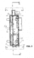
- Figure 2 is an elevational view of the printed circuit board and housing of Figure 1 as taken along line 2-2 of Figure 1;
- Figure 3A is a section view taken along
line 3A-3A of Figure 2; - Figure 3B is a plan view taken along
line 3B-3B of Figure 2; - Figure 3C is a partial plan view taken along
line 3C-3C of Figure 2; - Figure 4 is a greatly enlarged detail view of
region 4 of Figure 3A; - Figure 5 is a greatly enlarged detail view of region 5 of Figure 3B;
- Figure 6 shows an alternative embodiment for securing a circuit board against lateral movement;
- Figure 7 partially shows another alternative housing portion formed in accordance with the present development;
- Figure 8 is a sectional view of the housing portion of Figure 7 taken along line 8-8 and showing an associated circuit board installed therein.
- Figure 1 illustrates a printed circuit board PCB and enclosure housing portion H1 both formed in accordance with the present development and assembled according to the present development. In a typical arrangement, the enclosure housing portion H1 is adapted to be connected to a mating housing portion (partially shown schematically at H2 in Figure 3B) to enclose the printed circuit board PCB in a hollow interior space defined by the mated housing portions.
- Except as otherwise shown and/or described herein, the printed circuit board PCB, shown separately in Figure 1A, is conventional in all respects and comprises an relatively thin planar board member B having a front face BF and an opposite rear face BR on which electronic components are mounted and interconnected by traces that are also applied to the front and rear faces (the electronic components and traces are not shown herein in order to simplify the drawings). The front and rear faces BF,BR each comprise a contiguous area that is defined by a peripheral edge PE of the board. Similar to conventional printed circuit boards, the peripheral edge is dimensioned and conformed to fit closely within an enclosure housing such as that defined by the housing portions H1,H2. Unlike conventional printed circuit boards, however, the printed circuit board PCB comprises at least one and preferably at least two protruding tabs T1,T2 that project outwardly from and partially define the peripheral edge PE. The one or more tabs T1,T2 extend within the plane of the board B.
- With continuing reference to Figure 1A, the board B comprises a front edge FE and is intended to be inserted slidably into the housing portion H1 in an insertion direction I that is parallel to the plane of the board (the term "front" is used to simplify understanding of the development and is not intended to be limiting in terms of orientation of the housing portion H1 or board B). To facilitate this insertion operation, the peripheral edge PE comprises first and second opposite lateral edges L1,L2 that lie parallel to each other and to the insertion direction I and that are preferably smooth and linear. The tabs T1,T2 are preferably located opposite and in alignment with each other and comprise respective ramp surfaces TR1,TR2 that blend into the lateral edges L1,L2 and that are inclined in a direction opposite the insertion direction I (moving away from the board front edge FE). The ramp surfaces TR1,TR2 are terminated by respective locking faces TF1,TF2 that extend transversely inward toward each other from the outer terminal ends of the ramp surface TR1,TR2. In the illustrated embodiment, the locking faces TF1,TF2 extend normal to the insertion direction I. In addition, it is preferred that the locking faces TF1,TF2 blend into and partially define respective undercuts U1,U2 located adjacent the tabs T1,T2, immediately outward therefrom in terms of the insertion direction I. The undercuts U1,U2 preferably extend toward each other laterally inward relative to the lateral surfaces L1,L2, respectively.
- Referring now to both Figures 1 and 2, the housing portion H1 comprises at least one and typically multiple slots S1,S2, with each slot adapted to receive a printed circuit board PCB according to the present development (a board PCB is located in slot S1 but slot S2 is empty). As shown, the first slot S1 is defined by a first pair of opposed grooves G1a,G1b and a second slot S2 defined by a pair of opposed grooves G2a,G2b. In the illustrated embodiment, the grooves G1a,G1b,G2a,G2b are all identical to each other. The grooves G1a,G1b are aligned and lie parallel to each other, and the grooves G2a,G2b are aligned and lie parallel to each other so as to define the slots S1,S2 respectively therebetween for receiving a printed circuit board PCB with a close sliding fit. Each individual groove G1a,G1b,G2a,G2b preferably defines a width Gw (Figure 2) that is minimally larger than a thickness Bw of the board B to be received therein to minimize movement of the board in opposite directions transverse to the insertion direction I and plane of the board. Also, as best seen in Figure 3A, the grooves G1a,G1b (and also the grooves G2a,G2b) lie parallel and are spaced apart from each other a distance Gs that is minimally larger than the distance Ls defined between the board lateral edges L1,L2 so that the board B is closely received between the grooves G1a,G1b and is restrained against movement transverse to the insertion direction I and parallel to the plane of the board B. The grooves G1a,G1b need not be identical to each other and can vary in length. Also, the term "groove" is not intended to be limited to a continuous channel and can encompass any path that slidably receives the board B in the insertion direction I parallel to the plane of the board B and that prevents movement of the board transverse to the insertion direction. In another embodiment as shown in Fig. 6, the grooves G1a,G1b (only the groove G1a is shown) are defined as indicated by broken lines between a plurality of tabs Tg that project outwardly from an alternative housing portion H1'. Other arrangements are contemplated for inhibiting lateral or transverse movement of a board B relative to the insertion direction. Fig. 7 shows another alternative housing portion H1" wherein tabs Tg" project from an inner wall H1i" of the housing and are adapted to receive the front edge FE of board B therebetween. Also as shown in Fig. 7, the inner wall H1i" can include one or more slots Hs" for receiving a tab Tb (Fig. 8) that projects from front edge FE of board B.
- The housing portion H1 comprises latches that are adapted to retained the board tabs T1,T2 to lock each board B into a slot S1 or S2. The number of latches used to retain each board B should preferably equal the number of tabs T1,T2 defined by the board B. In the illustrated embodiment, the board B comprises two tabs T1,T2 and, as such, the illustrated housing portion H1 comprises first and second latches K1,K2 (see Figure 3A) associated with each slot S1,S2 to engage these tabs of the board, inserted therein.
- The structure and operation of the latches K1,K2 (referred to generally as latches K) as illustrated herein can be understood with reference to Figures 1 and 3A. There, the latches K1 for the slots S1,S2 are shown (the latches K2 for the slots S1,S2 are preferably identical to the latches K1). Preferably, the housing portion H1 is defined as a molded polymeric structure and the latches K are defined as a one-piece construction therewith. Most preferably, as shown in Figures 1 and 3A, the housing portion H1 comprises opposite side walls W1,W2, and latches K1 are defined by the wall W1, preferably within the thickness thereof as shown, while the latches K2 are defined by the wall W2, preferably within the thickness of same. Figures 1, 3A, 3B and 3C show that each latch K comprises an aperture A defined in a respective wall W1,W2 and that is adapted to receive and retain a tab T1,T2. The apertures A are located within or at least in alignment with the grooves G1a,G1b,G2a,G2b. As the circuit board B is inserted into the slots S1,S2 in the direction I, the ramp surfaces TR1,TR2 engage the sidewalls W1,W2, respectively, and resiliently urge them apart from each other so that the tabs T1,T2 are able to slide in the slot S1 or S2. When the tabs T1,T2 encounter the apertures A of the latches K1,K2, respectively, they are received therein so that the sidewalls W1,W2 are able contract inwardly toward each other under their own resilient bias and resume their normal shape. The apertures A are dimensioned to be larger than the board width Bw to ensure that the tabs T1,T2 are readily received therein even if slightly misaligned. It is notable that the resilient characteristics of the molded polymeric walls W1,W2 are used to retain a board B therebetween, rather than known designs that rely on projecting snap-legs that are less robust. Furthermore, the walls W1,W2 cooperate with each other to retain a board B therebetween, with each wall W1,W2 acting inwardly toward the other to increase resistance to board dislodgement. It should also be noted that the grooves G1a,G2a are preferably defined by and as a one-piece construction with the wall W1, while the grooves G1b,G2b are preferably defined by and as a one-piece construction with the wall W2. Furthermore, it is highly desirable that the apertures A extend entirely through the respective walls W1,W2 in which they are defined so as to allow for a visual confirmation that the tabs T1,T2 are firmly seated therein.
- With particular reference to Figures 4 and 5 the aperture A of each latch K is partially defined by a locking edge Ae that is arranged transverse (preferably perpendicular) to the board insertion direction I and that abuts or lies very close to the locking face TF1,TF2 of the tabs T1,T2 received therein to prevent sliding movement of the board B in a direction opposite the insertion direction I once the tab T1,T2 is received in the aperture (inward movement of the board B in the insertion direction I is limited by abutment of the front edge Fe or other portion of the board B with the housing H1 so that the tabs T1,T2 are aligned with the apertures A of the latches K1,K2, respectively, when the board B is fully installed so as to prevent over-insertion of the board B). The presence of undercuts U1,U2 in the peripheral edge PE of the board B facilitate separation of an installed board B from the housing portion H1 in that the separation operation typically requires that a blade be inserted between each tab T1,T2 and the locking edge Ae of each aperture or otherwise between the housing wall W1,W2 and board B so that the wall can be deformed outwardly to release the captured tab T1,T2.
- The invention has been described with reference to preferred embodiments. Modifications and alterations will occur to those of ordinary skill in the art, and it is intended that the claims be construed literally and/or according to the doctrine or equivalents to encompass all such modifications and alterations.
- In summary the invention discloses a enclosure housing has a first wall defined as a molded polymeric construction, a first latch defined as a one-piece construction with the first wall, a second wall defined as a molded polymeric construction, and a second latch defined as a one-piece construction with the second wall. A circuit board is connected to the enclosure housing and includes a board member defined by a periphery. The periphery includes: (i) a first tab defined by a first inclined ramp surface and a first locking face that lies transverse to the first inclined ramp surface, wherein the first tab is engaged with the first latch; and, (ii) a second tab defined by a second inclined ramp surface and a second locking face that lies transverse to the second inclined ramp surface, wherein the second tab is engaged with the second latch.
Claims (20)
- An enclosure housing portion adapted to receive and retain a circuit board, said enclosure housing portion comprising:a first side wall;a first latch defined as a one-piece construction with said first side wall, said first latch comprising an aperture adapted to receive a first projecting tab of an associated circuit board inserted into said housing portion.
- The enclosure housing portion as set forth in claim 1, wherein said first side wall and first latch are defined as a one-piece molded polymeric construction.
- The enclosure housing portion as set forth in claim 1 or 2, further comprising:a second side wall;a second latch defined as a one-piece construction with said second side wall, said second latch comprising an aperture adapted to receive a second projecting tab of an associated circuit board inserted into said housing portion.
- The enclosure housing portion as set forth in claim 3, wherein said first and second side walls and said first and second latches are all defined together as a one-piece molded polymeric construction.
- The enclosure housing portion as set forth in claim 3 or 4, further comprising structures adapted to inhibit movement of the associated circuit board in a direction transverse to an insertion direction in which the associated circuit board is inserted into the enclosure housing portion.
- The enclosure housing portion as set forth in claim 5, wherein said structures adapted to inhibit transverse movement comprise first and second grooves defined respectively by said first and second side walls, and wherein said aperture of said first latch is located in said first groove and said aperture of said second latch is located in said second groove.
- The enclosure housing portion as set forth in one of claims 3 to 6, wherein:said first and second grooves extend in said board insertion direction;said aperture of said first latch is partially defined by a first locking edge arranged transverse to said board insertion direction and that engages a locking face of a first projecting tab of an associated circuit board inserted into said slot; and,said aperture of said second latch is partially defined by a second locking edge arranged transverse to said board insertion direction and that engages a locking face of a second projecting tab of an associated circuit board inserted into said slot.
- The enclosure housing portion as set forth in claim 7, wherein said first and second latches are located in aligned opposed facing relation with each other.
- A circuit board comprising:a planar board member defined by a peripheral edge, said peripheral edge comprising:a front edge;first and second parallel spaced-apart lateral edges that extend transversely relative to said front edge;a first projecting tab defined by a first inclined ramp surface and a first locking face that terminates and lies transverse to said first inclined ramp surface.
- The circuit board as set forth in claim 9, further comprising:a second projecting tab defined by a second inclined ramp surface and a second locking face that terminates and lies transverse to said second inclined ramp surface.
- The circuit board as set forth in claim 9 or 10, wherein said first and second inclined ramp surfaces blend into said first and second lateral edges, respectively.
- The circuit board as set forth in claim 11, wherein said first and second locking faces lie normal to said first and second lateral edges.
- The circuit board as set forth in one of claims 9 to 12, wherein said circuit board is installed in an enclosure housing portion, said enclosure housing portion comprising:a first side wall;a first latch defined as a one-piece construction with said first side wall, said first latch comprising an aperture in which said first projecting tab is positioned.
- The circuit board as set forth in claim 13, wherein said first side wall and first latch of said enclosure housing portion are defined as a one-piece molded polymeric construction.
- The circuit board as set forth in claim 10, wherein said wherein said circuit board is installed in an enclosure housing portion, said enclosure housing portion comprising:a first side wall;a first latch defined as a one-piece construction with said first side wall, said first latch comprising an aperture in which said first projecting tab is positioned;a second side wall;a second latch defined as a one-piece construction with said second side wall, said second latch comprising an aperture in which said second projecting tab is positioned;
- The circuit board as set forth in claim 15, wherein said first and second side walls and said first and second latches of said enclosure housing portion are all defined together as a one-piece molded polymeric construction.
- The circuit board as set forth in claim 16, wherein said first and second side walls of said enclosure housing portion further define respective first and second grooves that cooperate to define a slot therebetween, and wherein said circuit board is located in said slot with said first and second lateral edges thereof seated in said first and second grooves, respectively.
- The circuit board as set forth in claim 17, wherein said enclosure housing portion is defined with said aperture of said first latch located in said first groove and said aperture of said second latch located in said second groove.
- The circuit board as set forth in claim 17, wherein:said first and second grooves extend in a board insertion direction;said aperture of said first latch is partially defined by a first locking edge arranged transverse to said board insertion direction and that engages a locking face of said first projecting tab of said circuit board; and,said aperture of said second latch is partially defined by a second locking edge arranged transverse to said board insertion direction and that engages a locking face of said second projecting tab of said circuit board.
- An enclosure housing portion comprising:a first side wall defined as a molded polymeric construction;a first latch defined as a one-piece construction with said first side wall;a second side wall defined as a molded polymeric construction;a second latch defined as a one-piece construction with said second side wall;a circuit board connected to said enclosure housing portion, said circuit board comprising a planar board member defined by a peripheral edge, said peripheral edge comprising: (i) a first projecting tab defined by a first inclined ramp surface and a first locking face that lies transverse to said first inclined ramp surface, wherein said first projecting tab is engaged with said first latch; and, (ii) a second projecting tab defined by a second inclined ramp surface and a second locking face that lies transverse to said second inclined ramp surface, wherein said second projecting tab is engaged with said second latch.
Applications Claiming Priority (1)
| Application Number | Priority Date | Filing Date | Title |
|---|---|---|---|
| US10/879,667 US7064951B2 (en) | 2004-06-29 | 2004-06-29 | Space effective structure and method for retaining printed circuit boards within a housing |
Publications (3)
| Publication Number | Publication Date |
|---|---|
| EP1613137A2 true EP1613137A2 (en) | 2006-01-04 |
| EP1613137A3 EP1613137A3 (en) | 2008-01-02 |
| EP1613137B1 EP1613137B1 (en) | 2010-12-08 |
Family
ID=35149085
Family Applications (1)
| Application Number | Title | Priority Date | Filing Date |
|---|---|---|---|
| EP05013988A Ceased EP1613137B1 (en) | 2004-06-29 | 2005-06-28 | Space effective structure and method for retaining printed circuit boards within a housing |
Country Status (4)
| Country | Link |
|---|---|
| US (1) | US7064951B2 (en) |
| EP (1) | EP1613137B1 (en) |
| JP (1) | JP2006019731A (en) |
| DE (1) | DE602005025176D1 (en) |
Families Citing this family (6)
| Publication number | Priority date | Publication date | Assignee | Title |
|---|---|---|---|---|
| BRPI0901450A2 (en) * | 2009-05-04 | 2011-01-18 | Weg Automacao S A | communication protocol interface module |
| SG180052A1 (en) * | 2010-10-28 | 2012-05-30 | Rockwell Automation Asia Pacific Business Ctr Pte Ltd | Programmable controller component with assembly alignment features |
| CN102789283A (en) * | 2011-05-20 | 2012-11-21 | 鸿富锦精密工业(深圳)有限公司 | Electronic device with power module |
| US9230765B2 (en) * | 2012-11-02 | 2016-01-05 | Rockwell Automation Technologies, Inc. | Modular overload relay assembly with mechanically isolated connector |
| EP3425756B1 (en) | 2017-07-07 | 2020-03-25 | Pepperl+Fuchs AG | Housing for receiving a printed circuit board having an overvoltage protection unit and overvoltage protection module |
| US10365696B1 (en) * | 2018-09-27 | 2019-07-30 | Moxa Inc. | Industrial input/output device with movable connector |
Citations (4)
| Publication number | Priority date | Publication date | Assignee | Title |
|---|---|---|---|---|
| DE3335820A1 (en) | 1983-10-01 | 1985-04-11 | Siemens AG, 1000 Berlin und 8000 München | Carrier for the attachment and positioning of printed-circuit boards |
| DE29607097U1 (en) | 1996-04-19 | 1996-07-04 | Abb Patent Gmbh, 68309 Mannheim | Arrangement for fixing a circuit board in a housing |
| DE19837974A1 (en) | 1998-08-21 | 2000-02-24 | Bosch Gmbh Robert | Electrical system casing for circuit boards that have casing mounting points; has shielding projections formed on casing |
| US6407926B1 (en) | 2000-09-18 | 2002-06-18 | Eaton Corporation | Apparatus for mounting electronic circuits in electric power equipment enclosures |
Family Cites Families (4)
| Publication number | Priority date | Publication date | Assignee | Title |
|---|---|---|---|---|
| US6324054B1 (en) * | 1998-01-26 | 2001-11-27 | Seagate Technology Llc | Wrap around shock absorber for disc drives |
| US6206730B1 (en) * | 1999-02-04 | 2001-03-27 | Molex Incorporated | Shielded electrical connector |
| TW508033U (en) * | 2001-10-12 | 2002-10-21 | Hon Hai Prec Ind Co Ltd | Optical transceiver module |
| US6957978B2 (en) * | 2003-07-31 | 2005-10-25 | Drew Zoller | Cord retainer |
-
2004
- 2004-06-29 US US10/879,667 patent/US7064951B2/en not_active Expired - Lifetime
-
2005
- 2005-06-28 JP JP2005187564A patent/JP2006019731A/en active Pending
- 2005-06-28 EP EP05013988A patent/EP1613137B1/en not_active Ceased
- 2005-06-28 DE DE602005025176T patent/DE602005025176D1/en not_active Expired - Lifetime
Patent Citations (4)
| Publication number | Priority date | Publication date | Assignee | Title |
|---|---|---|---|---|
| DE3335820A1 (en) | 1983-10-01 | 1985-04-11 | Siemens AG, 1000 Berlin und 8000 München | Carrier for the attachment and positioning of printed-circuit boards |
| DE29607097U1 (en) | 1996-04-19 | 1996-07-04 | Abb Patent Gmbh, 68309 Mannheim | Arrangement for fixing a circuit board in a housing |
| DE19837974A1 (en) | 1998-08-21 | 2000-02-24 | Bosch Gmbh Robert | Electrical system casing for circuit boards that have casing mounting points; has shielding projections formed on casing |
| US6407926B1 (en) | 2000-09-18 | 2002-06-18 | Eaton Corporation | Apparatus for mounting electronic circuits in electric power equipment enclosures |
Non-Patent Citations (1)
| Title |
|---|
| "Auxiliary Circuit board alignment system", RESEARCH DISCLOSURE, vol. 448, no. 15, August 2001 (2001-08-01) |
Also Published As
| Publication number | Publication date |
|---|---|
| EP1613137A3 (en) | 2008-01-02 |
| US7064951B2 (en) | 2006-06-20 |
| EP1613137B1 (en) | 2010-12-08 |
| DE602005025176D1 (en) | 2011-01-20 |
| JP2006019731A (en) | 2006-01-19 |
| US20050286237A1 (en) | 2005-12-29 |
Similar Documents
| Publication | Publication Date | Title |
|---|---|---|
| CA2577574C (en) | Circuit board connector extension | |
| US6655995B1 (en) | Electrical connector receptacle cage with interlocking upper and lower shells | |
| EP0580133B1 (en) | Electrical connector | |
| US7331822B2 (en) | Receptacle connector | |
| KR100666067B1 (en) | Electrical contact with orthogonal contact arm and offset contact area | |
| US6099351A (en) | Shielded electrical connector having a spacer with improved locking means for engagement within the connector | |
| US5772038A (en) | Parts transporting tray | |
| US5490802A (en) | Secondary terminal lock plug through stuffer | |
| US6035514A (en) | Guide piece and method for mounting to a chassis in multiple orientations | |
| WO2003061079A1 (en) | Floating interface for electrical connector | |
| EP0407864B1 (en) | Printed circuit board edge connector | |
| WO2000068867A1 (en) | One-piece electrical connector for the connection of a smart card | |
| EP1379116B1 (en) | Space-saving card guides for card cage and method of installing same on a card cage or frame | |
| US5738551A (en) | Retaining electrical connector | |
| US6017248A (en) | Card edge connector | |
| EP1613137B1 (en) | Space effective structure and method for retaining printed circuit boards within a housing | |
| CN111033907A (en) | Compact combined connector | |
| EP1054480A2 (en) | Electromagnetic interference shielding gasket | |
| US4530033A (en) | Card frame for circuit cards | |
| EP1006380B1 (en) | Electrical and/or optical connector | |
| US6106331A (en) | Connector assembly | |
| EP0779675A1 (en) | Wedge connector for electrical conductors | |
| EP0210686A2 (en) | Electrical connector with mounting members | |
| EP1408727B1 (en) | A plug-in card for electronic data-processing devices | |
| US4458972A (en) | Locking device for connecting means |
Legal Events
| Date | Code | Title | Description |
|---|---|---|---|
| PUAI | Public reference made under article 153(3) epc to a published international application that has entered the european phase |
Free format text: ORIGINAL CODE: 0009012 |
|
| AK | Designated contracting states |
Kind code of ref document: A2 Designated state(s): AT BE BG CH CY CZ DE DK EE ES FI FR GB GR HU IE IS IT LI LT LU MC NL PL PT RO SE SI SK TR |
|
| AX | Request for extension of the european patent |
Extension state: AL BA HR LV MK YU |
|
| PUAL | Search report despatched |
Free format text: ORIGINAL CODE: 0009013 |
|
| AK | Designated contracting states |
Kind code of ref document: A3 Designated state(s): AT BE BG CH CY CZ DE DK EE ES FI FR GB GR HU IE IS IT LI LT LU MC NL PL PT RO SE SI SK TR |
|
| AX | Request for extension of the european patent |
Extension state: AL BA HR LV MK YU |
|
| RIC1 | Information provided on ipc code assigned before grant |
Ipc: H05K 7/14 20060101ALI20071123BHEP Ipc: G06F 1/16 20060101AFI20071123BHEP |
|
| 17P | Request for examination filed |
Effective date: 20080605 |
|
| AKX | Designation fees paid |
Designated state(s): DE FR GB |
|
| 17Q | First examination report despatched |
Effective date: 20080818 |
|
| GRAP | Despatch of communication of intention to grant a patent |
Free format text: ORIGINAL CODE: EPIDOSNIGR1 |
|
| GRAC | Information related to communication of intention to grant a patent modified |
Free format text: ORIGINAL CODE: EPIDOSCIGR1 |
|
| GRAS | Grant fee paid |
Free format text: ORIGINAL CODE: EPIDOSNIGR3 |
|
| GRAA | (expected) grant |
Free format text: ORIGINAL CODE: 0009210 |
|
| AK | Designated contracting states |
Kind code of ref document: B1 Designated state(s): DE FR GB |
|
| REG | Reference to a national code |
Ref country code: GB Ref legal event code: FG4D |
|
| REF | Corresponds to: |
Ref document number: 602005025176 Country of ref document: DE Date of ref document: 20110120 Kind code of ref document: P |
|
| PLBE | No opposition filed within time limit |
Free format text: ORIGINAL CODE: 0009261 |
|
| STAA | Information on the status of an ep patent application or granted ep patent |
Free format text: STATUS: NO OPPOSITION FILED WITHIN TIME LIMIT |
|
| 26N | No opposition filed |
Effective date: 20110909 |
|
| REG | Reference to a national code |
Ref country code: DE Ref legal event code: R097 Ref document number: 602005025176 Country of ref document: DE Effective date: 20110909 |
|
| REG | Reference to a national code |
Ref country code: FR Ref legal event code: PLFP Year of fee payment: 11 |
|
| REG | Reference to a national code |
Ref country code: FR Ref legal event code: PLFP Year of fee payment: 12 |
|
| REG | Reference to a national code |
Ref country code: FR Ref legal event code: PLFP Year of fee payment: 13 |
|
| REG | Reference to a national code |
Ref country code: FR Ref legal event code: PLFP Year of fee payment: 14 |
|
| P01 | Opt-out of the competence of the unified patent court (upc) registered |
Effective date: 20230404 |
|
| PGFP | Annual fee paid to national office [announced via postgrant information from national office to epo] |
Ref country code: FR Payment date: 20230523 Year of fee payment: 19 Ref country code: DE Payment date: 20230523 Year of fee payment: 19 |
|
| PGFP | Annual fee paid to national office [announced via postgrant information from national office to epo] |
Ref country code: GB Payment date: 20230523 Year of fee payment: 19 |
|
| REG | Reference to a national code |
Ref country code: DE Ref legal event code: R119 Ref document number: 602005025176 Country of ref document: DE |
|
| GBPC | Gb: european patent ceased through non-payment of renewal fee |
Effective date: 20240628 |
|
| PG25 | Lapsed in a contracting state [announced via postgrant information from national office to epo] |
Ref country code: DE Free format text: LAPSE BECAUSE OF NON-PAYMENT OF DUE FEES Effective date: 20250101 |
|
| PG25 | Lapsed in a contracting state [announced via postgrant information from national office to epo] |
Ref country code: FR Free format text: LAPSE BECAUSE OF NON-PAYMENT OF DUE FEES Effective date: 20240630 |
|
| PG25 | Lapsed in a contracting state [announced via postgrant information from national office to epo] |
Ref country code: GB Free format text: LAPSE BECAUSE OF NON-PAYMENT OF DUE FEES Effective date: 20240628 |