-
The present invention relates to an electrophotograph
type color image forming device. More particularly, the
present invention relates to a device for stably supplying
a high voltage formed by superposing DC and AC voltages to
a plurality of developer units for respective colors,
regardless of load change, for color printing or copying.
-
Non-contact type color image forming devices comprise
fixed type developer units which maintain a predetermined
development gap of, for example, 0.2 mm without contacting
a developing roller with a photosensitive drum or without
separating the developing roller from the photosensitive
drum. The fixed type developer units can solve various
problems occurring in contact type developer units that
use an eccentric cam, a cam drive motor, and an electronic
clutch to transfer the developer for accommodating
respective developing agents of yellow, magenta, cyan, and
black, at the time of developing. In the aforementioned
non-contact type color image forming devices, a voltage
supply device for a developer unit comprises a high
voltage supply source for supplying high voltages to a
developing roller and a developing agent supply roller, a
fixed contact terminal of a fixed type developer unit, and
a printing circuit board (PCB) for transferring a high
voltage output from the high voltage supply source to the
fixed contact terminal of the developer unit.
-
In the non-contact type color image forming devices
using the fixed type developer unit, the developer is not
in contact with or separated from the photosensitive drum,
so that deterioration of image quality and shortened
lifetime of the photosensitive drum due to contact shock
can be suppressed. In addition, the voltage supply device
for the developer unit uses the PCB, so that a high
voltage transfer interval resulting in complicated wire
harnesses can be minimized.
-
However, in the above devices, a structure of the wire
harness for supplying a voltage from the high voltage
source, a structure of connecting lines patterned in the
PCB, and a structure of high voltage contacts for
switching a high voltage are still complicated.
Therefore, when the developers are exchanged, there is a
problem in that high voltage noise occurs and switching
reliability is lowered at the high voltage contacts.
-
Accordingly, a need exists for a system and method for
stably supplying a high voltage to a plurality of
developer units for respective colors, regardless of load
changes and having minimal high voltage noise.
-
According to the present invention there is provided
an apparatus and method as set forth in the appended
claims. Preferred features of the invention will be
apparent from the dependent claims, and the description
which follows.
-
The present invention provides a high voltage supply
source for color printing or copying in which at least two
sub high voltages having different voltage levels are
generated from a main high voltage using a Zener diode and
are then supplied to a developer unit.
-
The present invention further provides a high voltage
supply source for stably supplying a high voltage formed
by superposing DC and AC voltages to a plurality of
developer units, regardless of load changes.
-
According to an aspect of the present invention, a
high voltage supply device for a developer unit is
provided comprising a first sub high voltage generating
unit having at least one Zener diode for generating a
first sub high voltage from a main high voltage formed by
superposing a first DC and AC voltage, and applying the
first sub high voltage to a developing agent supply
roller, and a second sub high voltage generating unit
having at least one Zener diode for generating a second
sub high voltage from the main high voltage and applying
the second sub high voltage to a developing roller. The
voltage supply device further comprises a first current
stabilizing unit connected between a first sub high
voltage input contact of the first sub high voltage
generating unit and the developing agent supply roller and
a ground, and a second current stabilizing unit connected
between a second sub high voltage input contact of the
second sub high voltage generating unit and the developing
roller and the ground.
-
According to another aspect of the present invention,
a high voltage supply device is provided for a developer
unit comprising a main high voltage unit for generating a
main high voltage formed by superposing first DC and AC
voltages, a switch unit for switching in accordance with a
predetermined developing timing to supply the main high
voltage to one of the developer units for respective
colors, and a plurality of sub high voltage units for
generating stable first and second sub high voltages from
the main high voltage supplied from the switch unit,
regardless of load changes, and for supplying the stable
first and second sub high voltages to a developing agent
supply roller and a developing roller, respectively.
-
The above and other features and advantages of the
present invention will become more apparent by describing
in detail exemplary embodiments thereof with reference to
the attached drawings in which:
- Figure 1 is a block diagram illustrating a high
voltage supply device of a developer unit according to an
embodiment of the present invention;
- Figure 2 is a circuit diagram illustrating a detailed
construction of a sub high voltage unit of Figure 1
according to an embodiment of the present invention;
- Figures 3A to 3C are wave form diagrams illustrating a
main high voltage and first and second sub high voltages
of Figure 2 according to an embodiment of the present
invention; and
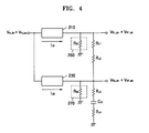
- Figure 4 is a circuit diagram for illustrating a
method of calculating a resistance value for stabilizing a
Zener current of Figure 2.
-
-
Throughout the drawings, like reference numerals will
be understood to refer to like parts, components and
structures.
-
The present invention will now be described in greater
detail with reference to the accompanying drawings.
-
A high voltage supply device for a developer unit
according to an embodiment of the present invention is
preferably provided with a non-contact type color image
forming device. The non-contact type color image forming
device comprises a fixed developer unit to maintain a
predetermined developing gap of, for example, 0.2 mm
without contacting a developing roller with a
photosensitive drum and without separating the developing
roller from the photosensitive drum. In order to perform
a developing process in a color laser beam printer using
the fixed developer unit, of which, the electric field is
inversely proportional to the developing gap, a toner
moves from the developing roller to the photosensitive
drum. The toner moves from the developing roller to the
photosensitive drum by supplying a high voltage formed by
superposing AC and DC voltages, to the developing agent
supply roller and the developing roller. When an AC
voltage is applied, a moving direction of the toner is
determined by a developing vector, that is, a DC component
of a developing bias - electric potential of a
photosensitive drum surface. When using a negatively
charged toner, if the developing vector is negatively
charged, the toner of the developing roller moves to a
photosensitive drum. If the developing vector is
positively charged, the toner of the developing roller
does not move.
-
Figure 1 is a block diagram illustrating a high
voltage supply device of a developer unit according to an
embodiment of the present invention. The high voltage
supply device for the developer unit comprises a main high
voltage unit 110, a switch unit 130, and a sub high
voltage unit 150. It is preferable that the sub high
voltage unit 150 be placed within the developer units 161,
163, 165, and 167 for respective colors so as to reduce
the number of high voltage output contacts in the switch
unit 130 and the number of high voltage input contacts in
the developer units 161, 163, 165, and 167.
-
The main high voltage unit 110 generates a main high
voltage by superposing first DC and AC voltages. A proper
range of the first DC and AC voltages constituting the
main high voltage is set to generate first and second sub
high voltages required for a developing roller 180, and a
developing agent supply roller 170, respectively, from the
main high voltage. The main high voltage generated from
the main high voltage unit 110 is supplied to the switch
unit 130 through a wiring harness between high voltage
output and input contacts T1 and T2, respectively.
-
The switch unit 130, having a solenoid 120 that
includes the high voltage input and output contacts T3 and
T4, respectively, selectively switches the main high
voltage supplied from the high voltage input contact T2 in
accordance with a predetermined developing timing to
supply a sub high voltage generated from the main high
voltage unit 110 to the developer units 161, 163, 165, and
167 for the respective colors. The sub high voltage is
provided to the developer units 161, 163, 165, and 167
through a wiring harness between high voltage output and
input contacts T5 and T6, respectively. The solenoid can
be comprised of, but not limited to, devices such as a
relay.
-
The sub high voltage unit 150 generates the stable
first and second sub high voltages, regardless of load
changes, from the main high voltage supplied from the
switch unit 130 to the high voltage input contact point
T6, and supplies the generated first and second sub high
voltages to the developing agent supply roller 170 and the
developing roller 180, respectively.
-
According to the aforementioned construction, by
generating and providing at least two sub high voltages
from one main high voltage supplied from the main high
voltage unit 110 to the developer units 161, 163, 165, and
167 for the respective colors, it is possible to
drastically reduce the number of high voltage wire
harnesses, pattern connection lines, and high voltage
switch contacts required for supplying a voltage from the
main high voltage unit 110 to the developer units 161,
163, 165, and 167 for the respective colors.
-
Figure 2 is a circuit diagram illustrating a detailed
construction example of the sub high voltage unit 150 of
Figure 1 according to an embodiment of the present
invention. The sub high voltage unit 150 comprises a
first sub high voltage generating unit 210, a second sub
high voltage generating unit 230, a first current
stabilizing unit 250, and a second current stabilizing
unit 270. Operation of the sub high voltage unit 150 will
now be described in greater detail with reference to the
waveform diagrams shown in Figures 3A to 3C.
-
Referring to Figure 2, a main high voltage that is
formed by superposing first DC and AC voltages Vm_dc and
Vm_pp, respectively, as shown in Figure 3A, is applied to
the first and second sub high voltage generating units 210
and 230.
-
The first sub high voltage generating unit 210
comprises at least one Zener diode, or more than one Zener
diode connected in series. In an embodiment of the
present invention, the first sub high voltage generating
unit 210 comprises the first and second backward Zener
diodes ZD1 and ZD2. The first and second Zener diodes ZD1
and ZD2 have a Zener voltage of 200V, for example. The
first and second Zener diodes ZD1 and ZD2 therefore,
provide a function of clipping 400V in a positive
direction for the first AC voltage Vm_pp. As a result, the
first sub high voltage generating unit 210 generates the
first sub high voltage shown in FIG. 3B by superposing the
first sub DC and AC voltages Vs1_dc and Vs1_pp, respectively,
and supplies the first sub high voltage to the developing
agent supply roller 170. The first sub DC voltage Vs1_dc
is decreased by 200V compared to the first DC voltage
Vm_dc. The first sub AC voltage Vs1_pp is decreased by 400
Vpp compared to the first AC voltage Vm_pp.
-
The second sub high voltage generating unit 230
comprises at least one Zener diode, or more than one Zener
diode connected in series. In an embodiment of the
present invention, the second sub high voltage generating
unit 230 comprises the third backward Zener diode ZD3, and
fourth and fifth forward Zener diodes ZD4 and ZD5. The
third Zener diode ZD3 has a Zener voltage of 100V, for
example. The fourth and fifth Zener diodes ZD4 and ZD5
have Zener voltages of 100V and 200V, for example,
respectively. The third Zener diode ZD3 therefore,
provides a function of clipping 100V in a positive
direction for the first AC voltage Vm_pp. The fourth and
fifth Zener diodes ZD4 and ZD5 provide a function of
clipping 300V in a negative direction for the first AC
voltage Vm_pp. As a result, the second sub high voltage
generating unit 230 generates the second sub high voltage
shown in Figure 3C by superposing the second sub DC and AC
voltages Vs2_dc and Vs2_pp, respectively, and supplies the
second sub high voltage to the developing roller 180. The
second sub DC voltage Vs2_dc is increased by 100V compared
to the first DC voltage Vm_dc. The second sub AC voltage
Vs2_pp is decreased by 400 Vpp compared to the first AC
voltage Vm_pp.
-
The second sub high voltage supplied to the developing
roller 180 is higher by 100V in the case of the second sub
DC voltage, and is decreased by 400V in the case of the
second sub AC voltage, as is the first sub high voltage
supplied to the developing agent supply roller 170. In an
embodiment of the present invention, the difference
between the first and second sub high voltages is 300V in
a DC voltage, and the first and the second sub high
voltages in an AC voltage are equal to each other.
-
The number and the connecting direction of the Zener
diodes ZD1, ZD2, ZD3, ZD4, and ZD5 comprising the first
and second sub high voltage generating units 210 and 230
are not limited to the above embodiments. Various
modifications in the number and the connecting directions
of the Zener diodes are possible according to a size of
the first DC and AC voltages constituting the main high
voltage, and a size of the first and second sub high
voltages required for the developing agent supply roller
170 and the developing roller 180.
-
The first current stabilizing unit 250 comprises at
least one resistor (not shown) connected in parallel to a
load resistor or resistance (not shown) that includes a
developing agent supply roller 170 resistance, a toner
resistance, or a developing roller 180 resistance. The
second current stabilizing unit 270 comprises at least one
resistor (not shown) connected in parallel to a load
resistor or resistance (not shown) that includes a
developing agent supply roller 170 resistance, a toner
resistance, or a developing roller 180 resistance. The
first and second current stabilizing units 250 and 270
have a function of allowing the Zener diodes ZD1, ZD2,
ZD3, ZD4, and ZD5 to conduct a predetermined range of
Zener current to facilitate the regulation of the Zener
diode, even in a case wherein the load resistance varies
as the developing agent supply roller 170 resistance, the
developing roller 180 resistance, or the ground terminal
changes. As a result, it is possible to prevent the
deterioration of print quality due to damage of
electrostatic latent images on the photosensitive drum, or
due to a discharge from the developing roller 180 to the
photosensitive drum caused by an unregulated voltage
exceeding a rating voltage applied to the developing agent
supply roller 170 and the developing roller 180.
-
Figure 4 is a diagram illustrating a method of
calculating resistance values of resistors comprising the
first and second current stabilizing units 250 and 270 for
stabilizing a Zener current of Figure 2.
-
A Zener current iz1 is conducted by the Zener diodes
ZD1 and ZD2 comprising the first sub high voltage
generating unit 210, and a Zener current iz2 is conducted
by the Zener diodes ZD3, ZD4, and ZD5 comprising the
second sub high voltage generating unit 230. Further,
resistance RL1, RL2, and RL3 represent a developing agent
supply roller 170 resistance, a toner resistance, and a
developing roller 180 resistance, respectively. A
capacitance CL1 is formed in a predetermined gap between
the developing roller 180 and the photosensitive drum.
The resistance RL4 represents a resistance of the
photosensitive drum. Accordingly, a combined impedance of
RL1 to RL4 and CL1 can be used to represent a load
resistance RL which can vary in accordance with changes of
toner characteristics, aging phenomenon, or changes of the
ground terminal.
-
A value of the first resistor Rs1 comprising the first
current stabilizing unit 250 and which can be connected in
parallel to the load resistance RL, is determined by a
minimum Zener current iz1_min of the Zener diodes ZD1 and
ZD2 comprising the first sub high voltage generating unit
210, and the first AC voltage Vm_pp value of the main high
voltage. The minimum Zener current iz1_min, which is a
lowest current value required for the normal regulation of
the Zener diodes, can be obtained from a part
specification of the Zener diodes. For example, when the
minimum Zener current iz1_min is 1 mA and the first AC
voltage Vm_pp is 2 KV, a value of the first resistor Rs1 is
2M ohm. Therefore, even if the load resistance RL varies,
a value of the total load resistor Rt, that is, a parallel
resistance value of the first resistor Rs1 and the load
resistance RL, is smaller than a value of the first
resistor Rs1, that is, 2M ohm. Therefore, a current
greater than the minimum Zener current iz1_min of the Zener
diode can be conducted by the Zener diodes ZD1 and ZD2.
-
A value of the second resistor Rs2 comprising the
second current stabilizing unit 270 can be determined by
the minimum Zener current iz2_min of the Zener diodes ZD3,
ZD4, and ZD5 comprising the second sub high voltage
generating unit 230 and the first AC voltage Vm_pp value of
the main high voltage.
-
Although the aforementioned exemplary embodiment
illustrates only the first sub high voltage for the
developing agent supply roller 170 and the second sub high
voltage for the developing roller 180, a third sub high
voltage for a developing agent layer restriction blade
(not shown) can also be generated by using the same method
and apparatus. In addition, the present invention may be
adapted to a laser beam printer using a multi pass method
or a single pass method.
-
As described above, according to embodiments of the
present invention, it is possible to generate the first
and second sub high voltages from the main high voltage
using a plurality of Zener diodes in the developer unit to
thereby reduce high voltage noise at the time of
exchanging the developer by additionally connecting a
resistance for stabilizing the Zener current between the
output and ground terminals of the first and second sub
high voltages. Embodiments of the present invention
further enhance the reliability in the switching operation
of high voltage contacts, and enhance the ability to
normally regulate the Zener diodes, even if load
resistance varies by changes in the developing agent
supply roller 170 resistance, the developing roller 180
resistance, or a ground line resistance. As a result,
since the stable first and second sub high voltages are
supplied to the developing agent supply roller 170 and the
developing roller 180, the developing operation can be
stably performed, so that it is possible to improve print
quality and to extend a lifetime of the photosensitive
drum.
-
Although a few preferred embodiments have been shown
and described, it will be appreciated by those skilled in
the art that various changes and modifications might be
made without departing from the scope of the invention, as
defined in the appended claims.
-
Attention is directed to all papers and documents
which are filed concurrently with or previous to this
specification in connection with this application and
which are open to public inspection with this
specification, and the contents of all such papers and
documents are incorporated herein by reference.
-
All of the features disclosed in this specification
(including any accompanying claims, abstract and
drawings), and/or all of the steps of any method or
process so disclosed, may be combined in any combination,
except combinations where at least some of such features
and/or steps are mutually exclusive.
-
Each feature disclosed in this specification
(including any accompanying claims, abstract and drawings)
may be replaced by alternative features serving the same,
equivalent or similar purpose, unless expressly stated
otherwise. Thus, unless expressly stated otherwise, each
feature disclosed is one example only of a generic series
of equivalent or similar features.
-
The invention is not restricted to the details of the
foregoing embodiment(s). The invention extends to any
novel one, or any novel combination, of the features
disclosed in this specification (including any
accompanying claims, abstract and drawings), or to any
novel one, or any novel combination, of the steps of any
method or process so disclosed.