EP1609881A1 - Tantalum spattering target and method of manufacturing the same - Google Patents
Tantalum spattering target and method of manufacturing the same Download PDFInfo
- Publication number
- EP1609881A1 EP1609881A1 EP04712763A EP04712763A EP1609881A1 EP 1609881 A1 EP1609881 A1 EP 1609881A1 EP 04712763 A EP04712763 A EP 04712763A EP 04712763 A EP04712763 A EP 04712763A EP 1609881 A1 EP1609881 A1 EP 1609881A1
- Authority
- EP
- European Patent Office
- Prior art keywords
- tantalum
- target
- forging
- annealing
- sputtering target
- Prior art date
- Legal status (The legal status is an assumption and is not a legal conclusion. Google has not performed a legal analysis and makes no representation as to the accuracy of the status listed.)
- Granted
Links
Images


Classifications
-
- C—CHEMISTRY; METALLURGY
- C23—COATING METALLIC MATERIAL; COATING MATERIAL WITH METALLIC MATERIAL; CHEMICAL SURFACE TREATMENT; DIFFUSION TREATMENT OF METALLIC MATERIAL; COATING BY VACUUM EVAPORATION, BY SPUTTERING, BY ION IMPLANTATION OR BY CHEMICAL VAPOUR DEPOSITION, IN GENERAL; INHIBITING CORROSION OF METALLIC MATERIAL OR INCRUSTATION IN GENERAL
- C23C—COATING METALLIC MATERIAL; COATING MATERIAL WITH METALLIC MATERIAL; SURFACE TREATMENT OF METALLIC MATERIAL BY DIFFUSION INTO THE SURFACE, BY CHEMICAL CONVERSION OR SUBSTITUTION; COATING BY VACUUM EVAPORATION, BY SPUTTERING, BY ION IMPLANTATION OR BY CHEMICAL VAPOUR DEPOSITION, IN GENERAL
- C23C14/00—Coating by vacuum evaporation, by sputtering or by ion implantation of the coating forming material
- C23C14/22—Coating by vacuum evaporation, by sputtering or by ion implantation of the coating forming material characterised by the process of coating
- C23C14/34—Sputtering
-
- C—CHEMISTRY; METALLURGY
- C23—COATING METALLIC MATERIAL; COATING MATERIAL WITH METALLIC MATERIAL; CHEMICAL SURFACE TREATMENT; DIFFUSION TREATMENT OF METALLIC MATERIAL; COATING BY VACUUM EVAPORATION, BY SPUTTERING, BY ION IMPLANTATION OR BY CHEMICAL VAPOUR DEPOSITION, IN GENERAL; INHIBITING CORROSION OF METALLIC MATERIAL OR INCRUSTATION IN GENERAL
- C23C—COATING METALLIC MATERIAL; COATING MATERIAL WITH METALLIC MATERIAL; SURFACE TREATMENT OF METALLIC MATERIAL BY DIFFUSION INTO THE SURFACE, BY CHEMICAL CONVERSION OR SUBSTITUTION; COATING BY VACUUM EVAPORATION, BY SPUTTERING, BY ION IMPLANTATION OR BY CHEMICAL VAPOUR DEPOSITION, IN GENERAL
- C23C14/00—Coating by vacuum evaporation, by sputtering or by ion implantation of the coating forming material
- C23C14/22—Coating by vacuum evaporation, by sputtering or by ion implantation of the coating forming material characterised by the process of coating
- C23C14/34—Sputtering
- C23C14/3407—Cathode assembly for sputtering apparatus, e.g. Target
- C23C14/3414—Metallurgical or chemical aspects of target preparation, e.g. casting, powder metallurgy
-
- B—PERFORMING OPERATIONS; TRANSPORTING
- B21—MECHANICAL METAL-WORKING WITHOUT ESSENTIALLY REMOVING MATERIAL; PUNCHING METAL
- B21J—FORGING; HAMMERING; PRESSING METAL; RIVETING; FORGE FURNACES
- B21J1/00—Preparing metal stock or similar ancillary operations prior, during or post forging, e.g. heating or cooling
- B21J1/02—Preliminary treatment of metal stock without particular shaping, e.g. salvaging segregated zones, forging or pressing in the rough
-
- B—PERFORMING OPERATIONS; TRANSPORTING
- B21—MECHANICAL METAL-WORKING WITHOUT ESSENTIALLY REMOVING MATERIAL; PUNCHING METAL
- B21J—FORGING; HAMMERING; PRESSING METAL; RIVETING; FORGE FURNACES
- B21J5/00—Methods for forging, hammering, or pressing; Special equipment or accessories therefor
-
- C—CHEMISTRY; METALLURGY
- C22—METALLURGY; FERROUS OR NON-FERROUS ALLOYS; TREATMENT OF ALLOYS OR NON-FERROUS METALS
- C22F—CHANGING THE PHYSICAL STRUCTURE OF NON-FERROUS METALS AND NON-FERROUS ALLOYS
- C22F1/00—Changing the physical structure of non-ferrous metals or alloys by heat treatment or by hot or cold working
- C22F1/16—Changing the physical structure of non-ferrous metals or alloys by heat treatment or by hot or cold working of other metals or alloys based thereon
- C22F1/18—High-melting or refractory metals or alloys based thereon
-
- C—CHEMISTRY; METALLURGY
- C23—COATING METALLIC MATERIAL; COATING MATERIAL WITH METALLIC MATERIAL; CHEMICAL SURFACE TREATMENT; DIFFUSION TREATMENT OF METALLIC MATERIAL; COATING BY VACUUM EVAPORATION, BY SPUTTERING, BY ION IMPLANTATION OR BY CHEMICAL VAPOUR DEPOSITION, IN GENERAL; INHIBITING CORROSION OF METALLIC MATERIAL OR INCRUSTATION IN GENERAL
- C23C—COATING METALLIC MATERIAL; COATING MATERIAL WITH METALLIC MATERIAL; SURFACE TREATMENT OF METALLIC MATERIAL BY DIFFUSION INTO THE SURFACE, BY CHEMICAL CONVERSION OR SUBSTITUTION; COATING BY VACUUM EVAPORATION, BY SPUTTERING, BY ION IMPLANTATION OR BY CHEMICAL VAPOUR DEPOSITION, IN GENERAL
- C23C14/00—Coating by vacuum evaporation, by sputtering or by ion implantation of the coating forming material
- C23C14/06—Coating by vacuum evaporation, by sputtering or by ion implantation of the coating forming material characterised by the coating material
- C23C14/14—Metallic material, boron or silicon
-
- H—ELECTRICITY
- H10—SEMICONDUCTOR DEVICES; ELECTRIC SOLID-STATE DEVICES NOT OTHERWISE PROVIDED FOR
- H10P—GENERIC PROCESSES OR APPARATUS FOR THE MANUFACTURE OR TREATMENT OF DEVICES COVERED BY CLASS H10
- H10P14/00—Formation of materials, e.g. in the shape of layers or pillars
- H10P14/20—Formation of materials, e.g. in the shape of layers or pillars of semiconductor materials
- H10P14/22—Formation of materials, e.g. in the shape of layers or pillars of semiconductor materials using physical deposition, e.g. vacuum deposition or sputtering
Definitions
- the present invention relates to a manufacturing method of a sputtering target by subjecting a molten and cast tantalum ingot or billet to processes such as forging, annealing and rolling, and to a tantalum sputtering target obtained thereby.
- the sputtering method for forming a film of materials such as metal or ceramics has been used in numerous fields such as electronics, corrosion resistant materials and ornaments, catalysts, as well as in the manufacture of cutting/grinding materials and abrasion resistant materials.
- this tantalum target is manufactured by forging and annealing (heat treatment) an ingot or billet formed by performing electron beam melting and casting to a tantalum material, and thereafter performing rolling and finish processing (mechanical processing, polishing, etc.) thereto.
- the forging performed to the ingot or billet for the manufacture thereof will destroy the cast structure, disperse or eliminate the pores and segregations, and, by further annealing this, recrystallization will occur, and the precision and strength of the structure can be improved to a certain degree.
- the tantalum raw material is subject to electronic beam melting and thereafter cast to prepare an ingot or billet, and subsequently subject to cold forging - recrystallization annealing at 1173K - cold forging - recrystallization annealing at 1173K - cold rolling - recrystallization annealing at 1173K - finish processing to form a target material.
- the molten and cast ingot or billet generally has a crystal grain diameter of 50mm or more.
- forging causes the primary crystal grains to be crushed, and, although it appears that they all disappear, at the subsequent recrystallization temperature of roughly 1173K, it is considered that the destruction of the primary crystals is incomplete, and some traces of primary crystals remain. This will not disappear even with the subsequent forging and recrystallization annealing, and it is considered that hetero-phase crystal grains assembled in a form of wrinkles are generated at the stage of the final finish processing.
- a recrystallized structure is an aggregate of individual crystals with respectively different plane orientations, and each crystal is divided by a grain boundary.
- the strain added to the object via plastic working such as cold rolling is absorbed in the primary crystals by the transgranular slip in a certain direction, and the strain is accumulated therein.
- Such strained primary crystals take on a network cell structure that is extremely fine with slightly different orientations aggregated with lattice defects such as transition, and are also separated into a plurality of different areas with significantly differing orientations.
- this kind of deformation structure is heated, the cells change into subgrains (recovery process) through the combination of transition or rearrangement.
- the change from a cell into a subgrain hardly involves any change in the measurement. And, it is considered that these subgrains are combined, and a specific subgrain grows to become a recrystallized core, corrodes the non-recrystallized portion, grows and promotes the recrystallization.
- an object of the present invention is to provide a tantalum sputtering target having a high deposition speed and excellent uniformity of film, producing less arcings and particles and having excellent film forming properties, and the method capable of stably manufacturing the target by improving and devising plastic working steps such as forging and rolling, and the heat treatment step.
- the present invention provides:
- the sputtering target of the present invention is manufactured with the following process.
- a tantalum raw material usually, high purity tantalum of 4N5N or more is used
- this ingot or billet is subject to a series of processing steps including cold forging, rolling, annealing (heat treatment), finish processing and so on.
- the recrystallization annealing step at a temperature of 1373K to 1673K may be performed only once, by repeating this twice, the structural defects can be effectively reduced.
- the forging or rolling performed to the ingot or billet will destroy the cast structure, disperse or eliminate the pores and segregations, and, by further annealing this, recrystallization will occur, and the precision and strength of the structure can be improved to a certain degree by repeating clod forging or cold rolling and recrystallization annealing.
- the present invention it is desirable to obtain a material ultimately subject to plastic working such as cold rolling as described above, or to perform annealing at a temperature of 1173K or less after the final plastic working process such as rolling.
- a material ultimately subject to plastic working such as cold rolling as described above
- annealing at a temperature of 1173K or less after the final plastic working process such as rolling.
- finish processing machining or the like
- the structure obtained thereby is a non-recrystallized structure, and a processed structure remains therein.
- the structure (annealed at 1073K) having the non-recrystallized structure of the present invention is shown in FIG. 1 (magnification ⁇ 100) and FIG. 2 (magnification ⁇ 50).
- a conventional recrystallized structure (subject to recrystallization annealing at 1373K) is shown in FIG. 3 (magnification ⁇ 100) and FIG. 4 (magnification ⁇ 50).
- the structure of the tantalum target according to the present invention is clearly different from the conventional recrystallized structure.
- the strain added to the object is absorbed in the primary crystals by the transgranular slip in a certain direction, the strain is accumulated therein, and the subgrains have a structure before the crystal growth separated into different regions in slightly different directions divided with a plurality of transitions in this strained primary crystal.
- a target finished with plastic working such as rolling without being subject to annealing generates strain due to the heat from the sputtering operation depending on the processing conditions, and warping (bending) or cracks may occur. Still, if significant strain is not generated, it may be used as a target as a matter of course.
- This target material will have a Vickers hardness of 90 or more, Vickers hardness of 100 or more, or Vickers hardness of 125 or more, and a target superior in strength can be obtained.
- the tantalum sputtering target of the present invention has a characteristic non-recrystallized structure obtained from the foregoing manufacturing process.
- a tantalum raw material having a purity of 99.997% was subject to electron beam melting, and this was cast to prepare an ingot or billet having a thickness of 200mm and diameter of 200mmg ⁇ .
- the crystal grain diameter in this case was approximately 55mm.
- this was subject to recrystallization annealing at a temperature of 1500K.
- a material having a structure in which the average crystal grain diameter is 200 ⁇ m, thickness of 100mm, and diameter of 100mm ⁇ was obtained.
- the non-recrystallized structure referred to in this Description is a structure in which the grain boundary is unclear, or a structure where the grain boundary is twisting in a curved line, or both, as represented in FIG. 1 and FIG. 2, and the percentage (%) is defined by subtracting the area ratio of the obvious recrystallized portion as represented in FIG. 3 and FIG. 4 from 100%.
- the sheet resistance depends on the film thickness
- distribution of the sheet resistance within the wafer (8 inch) was measured, and the status of film thickness distribution was examined thereby. Specifically, the sheet resistance at 49 points on the wafer was measured, and the standard deviation ( ⁇ ) was calculated.
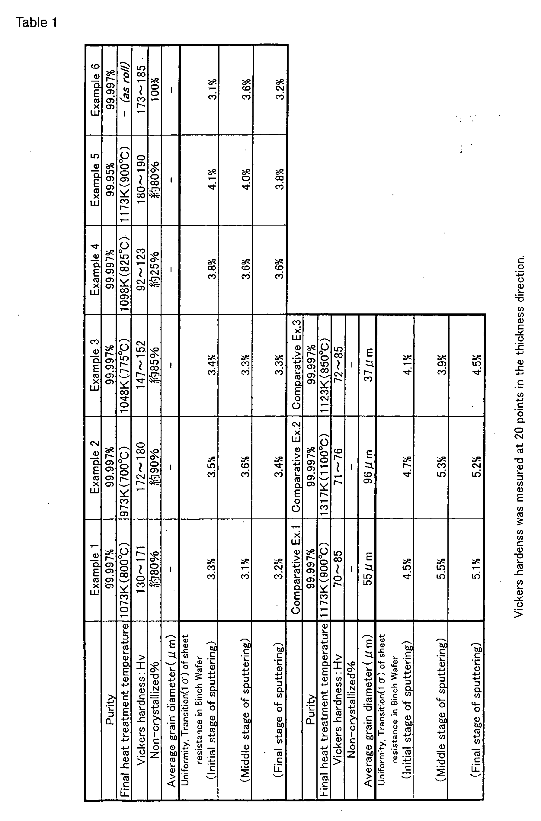
- Example 1 variation in the resistance distribution within the sheet from the initial stage of sputtering to the final stage of sputtering was small (3.1 to 3.3%); that is, variation in the film thickness distribution was small.
- the tantalum target of Example 1 has a high deposition speed, favorable film uniformity, little variation in the film thickness with an 8-inch wafer, and no generation of arcings or particles, and was therefore capable of improving the quality of sputtering deposition.
- FIG. 5 shows an erosion profile ( ⁇ points), and this standard and typical erosion profile is characterized in that the performance of the target is also favorable.
- a tantalum raw material having a purity of 99.997% was subject to electron beam melting, and this was cast to prepare an ingot or billet having a thickness of 200 mm and diameter of 200mm ⁇ .
- the crystal grain diameter in this case was approximately 50mm.
- this was subject to recrystallization annealing at a temperature of 1500K.
- a material having a structure in which the average crystal grain diameter is 200 ⁇ m, thickness of 100mm, and diameter of 100mm ⁇ was obtained.
- Example 2 As a result of performing the foregoing process, it was possible to obtain a tantalum target having a non-recrystallized structure of roughly 90% and which has a Vickers hardness Hv of 172 to 180. Further, the micrograph of this tantalum target obtained in Example 2 had the same crystal structure as the tantalum target shown in FIG. 1 and FIG. 2. The results are shown in Table 1 as with Example 1.
- the sheet resistance depends on the film thickness
- distribution of the sheet resistance within the wafer (8 inch) was measured, and the status of film thickness distribution was examined thereby. Specifically, the sheet resistance at 49 points on the wafer was measured, and the standard deviation ( ⁇ ) was calculated.
- this target had a high deposition speed, favorable film uniformity, little variation in the film thickness with an 8-inch wafer, and no generation of arcings or particles, and was therefore capable of improving the quality of sputtering deposition.
- the performance of the target was also favorable as with Example 1.
- a tantalum raw material having a purity of 99.997% was subject to electron beam melting, and this was cast to prepare an ingot or billet having a thickness of 200 mm and diameter of 300mm ⁇ .
- the crystal grain diameter in this case was approximately 50mm.
- this was subject to recrystallization annealing at a temperature of 1500K.
- a material having a structure in which the average crystal grain diameter is 250 ⁇ m, thickness of 100mm, and diameter of 100mm ⁇ was obtained.
- Example 3 As a result of performing the foregoing process, it was possible to obtain a tantalum target having a non-recrystallized structure of roughly 85% and which has a Vickers hardness Hv of 147 to 152. Further, the micrograph of this tantalum target obtained in Example 3 had the same crystal structure as the tantalum target shown in FIG. 1 and FIG. 2. The results are shown in Table 1 as with Example 1.
- the sheet resistance depends on the film thickness
- distribution of the sheet resistance within the wafer (8 inch) was measured, and the status of film thickness distribution was examined thereby. Specifically, the sheet resistance at 49 points on the wafer was measured, and the standard deviation ( ⁇ ) was calculated.
- Example 3 variation in the resistance distribution within the sheet from the initial stage of sputtering to the final stage of sputtering was small (3.4 to 3.3%); that is, variation in the film thickness distribution was small.
- this target had a high deposition speed, favorable film uniformity, little variation in the film thickness with an 8-inch wafer, and no generation of arcings or particles, and was therefore capable of improving the quality of sputtering deposition.
- the performance of the target was also favorable as with Example 1.
- a tantalum raw material having a purity of 99.997% was subject to electron beam melting, and this was cast to prepare an ingot or billet having a thickness of 200 mm and diameter of 300mm ⁇ .
- the crystal grain diameter in this case was approximately 50mm.
- this was subject to recrystallization annealing at a temperature of 1500K.
- a material having a structure in which the average crystal grain diameter is 250 ⁇ m, thickness of 100mm, and diameter of 100mm ⁇ was obtained.
- Example 4 As a result of performing the foregoing process, it was possible to obtain a tantalum target having a non-recrystallized structure of roughly 25% and which has a Vickers hardness Hv of 92 to 123. Further, the micrograph of this tantalum target obtained in Example 4 had the same crystal structure as the tantalum target shown in FIG. 1 and FIG. 2. The results are shown in Table 1 as with Example 1.
- the sheet resistance depends on the film thickness
- distribution of the sheet resistance within the wafer (8 inch) was measured, and the status of film thickness distribution was examined thereby. Specifically, the sheet resistance at 49 points on the wafer was measured, and the standard deviation ( ⁇ ) was calculated.
- this target had a high deposition speed, favorable film uniformity, little variation in the film thickness with an 8-inch wafer, and no generation of arcings or particles, and was therefore capable of improving the quality of sputtering deposition.
- the performance of the target was also favorable as with Example 1.
- a tantalum raw material having a purity of 99.95% was subject to electron beam melting, and this was cast to prepare an ingot or billet having a thickness of 200 mm and diameter of 300mm ⁇ .
- the crystal grain diameter in this case was approximately 50mm.
- this was subject to recrystallization annealing at a temperature of 1500K.
- a material having a structure in which the average crystal grain diameter is 250 ⁇ m, thickness of 100mm, and diameter of 100mm ⁇ was obtained.
- Example 5 As a result of performing the foregoing process, it was possible to obtain a tantalum target having a non-recrystallized structure of roughly 80% and which has a Vickers hardness Hv of 180 to 190. Further, the micrograph of this tantalum target obtained in Example 5 had the same crystal structure as the tantalum target shown in FIG. 1 and FIG. 2. The results are shown in Table 1 as with Example 1.
- the sheet resistance depends on the film thickness
- distribution of the sheet resistance within the wafer (8 inch) was measured, and the status of film thickness distribution was examined thereby. Specifically, the sheet resistance at 49 points on the wafer was measured, and the standard deviation ( ⁇ ) was calculated.
- Example 5 variation in the resistance distribution within the sheet from the initial stage of sputtering to the final stage of sputtering was small (3.8 to 4.1 %); that is, variation in the film thickness distribution was small.
- this target had a high deposition speed, favorable film uniformity, little variation in the film thickness with an 8-inch wafer, and no generation of arcings or particles, and was therefore capable of improving the quality of sputtering deposition.
- the performance of the target was also favorable as with Example 1.
- a tantalum raw material having a purity of 99.997% was subject to electron beam melting, and this was cast to prepare an ingot or billet having a thickness of 200mm and diameter of 300mm ⁇ .
- the crystal grain diameter in this case was approximately 50mm.
- this was subject to recrystallization annealing at a temperature of 1500K.
- a material having a structure in which the average crystal grain diameter is 200 ⁇ m, thickness of 100mm, and diameter of 100mm ⁇ was obtained.
- Example 6 As a result of performing the foregoing process, it was possible to obtain a tantalum target naturally having a non-recrystallized structure of roughly 100% and which has a Vickers hardness Hv of 173 to 185. Further, the micrograph of this tantalum target obtained in Example 6 had the same crystal structure as the tantalum target shown in FIG. 1 and FIG. 2. The results are shown in Table 1 as with Example 1.
- the sheet resistance depends on the film thickness
- distribution of the sheet resistance within the wafer (8 inch) was measured, and the status of film thickness distribution was examined thereby. Specifically, the sheet resistance at 49 points on the wafer was measured, and the standard deviation ( ⁇ ) was calculated.
- Example 6 variation in the resistance distribution within the sheet from the initial stage of sputtering to the final stage of sputtering was small (3.1 to 3.6%); that is, variation in the film thickness distribution was small.
- this target had a high deposition speed, favorable film uniformity, little variation in the film thickness with an 8-inch wafer, and no generation of arcings or particles, and was therefore capable of improving the quality of sputtering deposition.
- the performance of the target was also favorable as with Example 1.
- Example 2 As with Example 1, a tantalum raw material having a purity of 99.997% was subject to electron beam melting, and this was cast to prepare an ingot or billet having a thickness of 200 mm and diameter of 200mm ⁇ .
- the crystal grain diameter in this case was approximately 55mm.
- this was subject to recrystallization annealing at a temperature of 1173K.
- a material having a structure in which the average crystal grain diameter is 180 ⁇ m, thickness of 100mm, and diameter of 100mm ⁇ was obtained.
- the average crystal grain size was large at 55 ⁇ m and varied, and the orientation was roughly uniform from the target surface to the center portion thereof.
- the Vickers hardness Hv was 70 to 85, and the strength was weak.
- Comparative Example 1 of Table 1 The results shown in Comparative Example 1 of Table 1 were obtained by measuring the sheet resistance at 49 points on the wafer (8 inch) as with Example 1, and calculating the standard deviation ( ⁇ ) thereof.
- variation in the resistance distribution within the sheet from the initial stage of sputtering to the final stage of sputtering was large (4.5 to 5.5%); that is, variation in the film thickness distribution was significant.
- Example 2 As with Example 1, a tantalum raw material having a purity of 99.997% was subject to electron beam melting, and this was cast to prepare an ingot or billet having a thickness of 200 mm and diameter of 200mm ⁇ .
- the crystal grain diameter in this case was approximately 55mm.
- this was subject to recrystallization annealing at a temperature of 1173K.
- a material having a structure in which the average crystal grain diameter is 180 ⁇ m, thickness of 100mm, and diameter of 100mm ⁇ was obtained.
- the tantalum target obtained with the foregoing process had coarsened crystals. Further, the micrograph of the tantalum target obtained in Comparative Example 2 had the same crystal structure as the tantalum target shown in FIG. 3 and FIG. 4.
- the average crystal grain size was large at 96 ⁇ m and varied, and the orientation was roughly uniform from the target surface to the center portion thereof.
- the Vickers hardness Hv was 71 to 76, and the strength was weak.
- Comparative Example 2 of Table 1 The results shown in Comparative Example 2 of Table 1 were obtained by measuring the sheet resistance at 49 points on the wafer (8 inch) as with Example 1, and calculating the standard deviation ( ⁇ ) thereof.
- ⁇ standard deviation
- Example 2 As with Example 1, a tantalum raw material having a purity of 99.997% was subject to electron beam melting, and this was cast to prepare an ingot or billet having a thickness of 200 mm and diameter of 200mm ⁇ .
- the crystal grain diameter in this case was approximately 55mm.
- this was subject to recrystallization annealing at a temperature of 1173K.
- a material having a structure in which the average crystal grain diameter is 180 ⁇ m, thickness of 100mm, and diameter of 100mm ⁇ was obtained.
- the tantalum target obtained with the foregoing process had coarsened crystals. Further, the micrograph of the tantalum target obtained in Comparative Example 3 had the same crystal structure as the tantalum target shown in FIG. 3 and FIG. 4.
- the average crystal grain size was large at 37 ⁇ m and varied, and the orientation was roughly uniform from the target surface to the center portion thereof.
- the Vickers hardness Hv was 72 to 85, and the strength was weak.
- Comparative Example 3 of Table 1 were obtained by measuring the sheet resistance at 49 points on the wafer (8 inch) as with Example 1, and calculating the standard deviation ( ⁇ ) thereof.
- the present invention provides a tantalum target comprising a non-recrystallized structure without any coarsened abnormal crystals caused by the conventional recrystallization annealing or hetero-phase crystal grains aggregated in the form of wrinkles, and yields a superior effect in that it is capable of stably obtaining a tantalum sputtering target having a high deposition speed and excellent uniformity of film, producing less arcings and particles and having excellent film forming properties by performing plastic working such as forging and rolling and heat treatment, thereafter performing cold plastic working such as cold rolling , and performing annealing after such plastic working or final processing.
Landscapes
- Chemical & Material Sciences (AREA)
- Engineering & Computer Science (AREA)
- Mechanical Engineering (AREA)
- Materials Engineering (AREA)
- Metallurgy (AREA)
- Organic Chemistry (AREA)
- Chemical Kinetics & Catalysis (AREA)
- Physics & Mathematics (AREA)
- Thermal Sciences (AREA)
- Crystallography & Structural Chemistry (AREA)
- Physical Vapour Deposition (AREA)
- Forging (AREA)
Abstract
Description
Claims (12)
- A tantalum sputtering target manufactured by subjecting a molten and cast tantalum ingot or billet to plastic working such as forging, annealing and rolling, wherein the structure of the tantalum target comprises a non-recrystallized structure.
- The tantalum sputtering target according to claim 1, wherein the non-recrystallized structure is 20% or more.
- The tantalum sputtering target according to claim 1, wherein the non-recrystallized structure is 40% or more.
- The tantalum sputtering target according to any one of claims 1 to 3, wherein the tantalum target has a Vickers hardness of 90 or more.
- The tantalum sputtering target according to any one of claims 1 to 3, wherein the tantalum target has a Vickers hardness of 100 or more.
- The tantalum sputtering target according to any one of claims 1 to 3, wherein the tantalum target has a Vickers hardness of 125 or more.
- A manufacturing method of a tantalum sputtering target comprising a non-recrystallized structure by subjecting a molten and cast tantalum ingot or billet to processes such as forging, annealing and rolling, wherein plastic working is ultimately performed thereto.
- A manufacturing method of a tantalum sputtering target comprising a non-recrystallized structure by subjecting a molten and cast tantalum ingot or billet to processes such as forging, annealing and rolling, wherein, after the ultimate plastic working process, this is further subject to annealing at a temperature of 1173K or less.
- The manufacturing method of a tantalum sputtering target according to claim 7 or claim 8, wherein, after the ultimate plastic working process or after the annealing process, the finish processing is performed to form a target shape.
- The manufacturing method of a tantalum sputtering target according to any one of claims 7 to 9, wherein, during the processing stage, forging and recrystallization annealing are repeated two or more times.
- The manufacturing method of a tantalum sputtering target according to any one of claims 7 to 10, wherein extend forging and upset forging are repeatedly performed.
- The manufacturing method of a tantalum sputtering target according to any one of claims 7 to 11, wherein, after forging ingot or billet, during the processing stage, recrystallization annealing is performed at a temperature between the recrystallization temperature and 1673K.
Priority Applications (1)
| Application Number | Priority Date | Filing Date | Title |
|---|---|---|---|
| EP10175315.0A EP2253731B1 (en) | 2003-04-01 | 2004-02-19 | Tantalum spattering target |
Applications Claiming Priority (3)
| Application Number | Priority Date | Filing Date | Title |
|---|---|---|---|
| JP2003097659 | 2003-04-01 | ||
| JP2003097659 | 2003-04-01 | ||
| PCT/JP2004/001915 WO2004090193A1 (en) | 2003-04-01 | 2004-02-19 | Tantalum spattering target and method of manufacturing the same |
Related Child Applications (2)
| Application Number | Title | Priority Date | Filing Date |
|---|---|---|---|
| EP10175315.0A Division EP2253731B1 (en) | 2003-04-01 | 2004-02-19 | Tantalum spattering target |
| EP10175315.0 Division-Into | 2010-09-03 |
Publications (3)
| Publication Number | Publication Date |
|---|---|
| EP1609881A1 true EP1609881A1 (en) | 2005-12-28 |
| EP1609881A4 EP1609881A4 (en) | 2008-08-13 |
| EP1609881B1 EP1609881B1 (en) | 2011-04-20 |
Family
ID=33156648
Family Applications (2)
| Application Number | Title | Priority Date | Filing Date |
|---|---|---|---|
| EP10175315.0A Expired - Lifetime EP2253731B1 (en) | 2003-04-01 | 2004-02-19 | Tantalum spattering target |
| EP04712763A Expired - Lifetime EP1609881B1 (en) | 2003-04-01 | 2004-02-19 | Method of manufacturing a tantalum sputtering target |
Family Applications Before (1)
| Application Number | Title | Priority Date | Filing Date |
|---|---|---|---|
| EP10175315.0A Expired - Lifetime EP2253731B1 (en) | 2003-04-01 | 2004-02-19 | Tantalum spattering target |
Country Status (8)
| Country | Link |
|---|---|
| US (1) | US8172960B2 (en) |
| EP (2) | EP2253731B1 (en) |
| JP (2) | JP4256388B2 (en) |
| KR (1) | KR100698745B1 (en) |
| CN (2) | CN103966561A (en) |
| DE (1) | DE602004032323D1 (en) |
| TW (1) | TWI281507B (en) |
| WO (1) | WO2004090193A1 (en) |
Cited By (2)
| Publication number | Priority date | Publication date | Assignee | Title |
|---|---|---|---|---|
| EP2253730A3 (en) * | 2003-11-06 | 2011-01-19 | Nippon Mining & Metals Co., Ltd. | Tantalum sputtering target |
| CN102658346A (en) * | 2012-04-06 | 2012-09-12 | 宁夏东方钽业股份有限公司 | Forging method of large tantalum targets |
Families Citing this family (38)
| Publication number | Priority date | Publication date | Assignee | Title |
|---|---|---|---|---|
| JP4109901B2 (en) | 2001-05-29 | 2008-07-02 | キヤノン株式会社 | Image display device |
| WO2003046250A1 (en) * | 2001-11-26 | 2003-06-05 | Nikko Materials Company, Limited | Sputtering target and production method therefor |
| JP4883546B2 (en) * | 2002-09-20 | 2012-02-22 | Jx日鉱日石金属株式会社 | Method for manufacturing tantalum sputtering target |
| JP4263900B2 (en) * | 2002-11-13 | 2009-05-13 | 日鉱金属株式会社 | Ta sputtering target and manufacturing method thereof |
| EP1876258A4 (en) * | 2005-04-28 | 2008-08-13 | Nippon Mining Co | SPRAY TARGET |
| JP4949259B2 (en) * | 2005-10-04 | 2012-06-06 | Jx日鉱日石金属株式会社 | Sputtering target |
| JP4974362B2 (en) * | 2006-04-13 | 2012-07-11 | 株式会社アルバック | Ta sputtering target and manufacturing method thereof |
| JP5187713B2 (en) * | 2006-06-09 | 2013-04-24 | 国立大学法人電気通信大学 | Metal material refinement processing method |
| CN102356179B (en) | 2009-05-22 | 2013-10-30 | 吉坤日矿日石金属株式会社 | Tantalum sputtering target |
| KR101133029B1 (en) * | 2009-07-09 | 2012-04-04 | 한국생산기술연구원 | HIGH PURITY Ta SHEET AND MANUFACTURING METHOD OF THE SAME |
| KR101338758B1 (en) | 2009-08-11 | 2013-12-06 | 제이엑스 닛코 닛세키 킨조쿠 가부시키가이샤 | Tantalum sputtering target |
| KR20150039218A (en) | 2009-11-17 | 2015-04-09 | 가부시끼가이샤 도시바 | Tantalum sputtering target, method for manufacturing tantalum sputtering target, and method for manufacturing semiconductor device |
| KR20130008089A (en) | 2010-08-09 | 2013-01-21 | 제이엑스 닛코 닛세키 킨조쿠 가부시키가이샤 | Tantalum spattering target |
| KR101374281B1 (en) * | 2011-09-19 | 2014-04-09 | (주)나인디지트 | SPUTTERING TARGET Ta SHEET AND MANUFACTURING METHOD OF THE SAME |
| US20140242401A1 (en) | 2011-11-30 | 2014-08-28 | Jx Nippon Mining & Metals Corporation | Tantalum Sputtering Target and Method for Manufacturing Same |
| CN102517550B (en) * | 2011-12-20 | 2014-07-09 | 宁波江丰电子材料有限公司 | High purity tantalum target and preparation process thereof |
| CN104204282B (en) | 2012-03-21 | 2017-05-24 | 吉坤日矿日石金属株式会社 | Tantalum sputtering target, method for manufacturing same, and barrier film for semiconductor wiring formed by using target |
| EP2878700B1 (en) | 2012-12-19 | 2021-01-20 | JX Nippon Mining & Metals Corporation | Method for producing tantalum sputtering target |
| KR101950549B1 (en) | 2012-12-19 | 2019-02-20 | 제이엑스금속주식회사 | Tantalum sputtering target and method for producing same |
| KR20170092706A (en) | 2013-03-04 | 2017-08-11 | 제이엑스금속주식회사 | Tantalum sputtering target and production method therefor |
| CN103243285B (en) * | 2013-05-27 | 2015-08-26 | 宁夏东方钽业股份有限公司 | A kind of tantalum tungsten material and preparation method thereof |
| KR20160052664A (en) | 2013-10-01 | 2016-05-12 | 제이엑스 킨조쿠 가부시키가이샤 | Tantalum sputtering target |
| WO2015146516A1 (en) | 2014-03-27 | 2015-10-01 | Jx日鉱日石金属株式会社 | Tantalum sputtering target and production method therefor |
| CN104313600B (en) * | 2014-09-28 | 2016-08-24 | 燕山大学 | Impaired titanium alloy forging continuous point type forging and stamping Laser forming repair method |
| CN105722355B (en) * | 2014-12-05 | 2020-01-21 | 宏达国际电子股份有限公司 | Electronic device shell and processing method thereof |
| CN104741872B (en) * | 2015-01-16 | 2017-06-16 | 宁夏东方钽业股份有限公司 | A kind of preparation method of tantalum target |
| US10570505B2 (en) | 2015-05-22 | 2020-02-25 | JX Nippon Mining & Materials Corporation | Tantalum sputtering target, and production method therefor |
| KR20170091738A (en) | 2015-05-22 | 2017-08-09 | 제이엑스금속주식회사 | Tantalum sputtering target, and production method therefor |
| WO2018179742A1 (en) | 2017-03-30 | 2018-10-04 | Jx金属株式会社 | Tantalum sputtering target |
| CN109338316B (en) * | 2018-09-12 | 2020-04-28 | 中南大学 | Ultra-pure tantalum with controllable structure and texture and preparation method and application thereof |
| KR102078068B1 (en) * | 2018-10-26 | 2020-02-17 | 한국생산기술연구원 | Drawing dies for drawing of tantalum ingot and manufacturing method of tantalum ingot and tantalum wire |
| CN113025972B (en) * | 2021-03-01 | 2023-09-08 | 宁波江丰电子材料股份有限公司 | Manufacturing method of aluminum target |
| CN113755801B (en) * | 2021-09-17 | 2023-03-28 | 福州大学 | Preparation method of high-purity aluminum target material with uniform orientation |
| CN114164406B (en) * | 2021-11-30 | 2023-10-20 | 西北核技术研究所 | Particle pressed diode anode target for pulse power device and preparation method |
| CN114892136A (en) * | 2022-05-25 | 2022-08-12 | 同创(丽水)特种材料有限公司 | Tantalum target material and preparation method and application thereof |
| CN115044876A (en) * | 2022-06-02 | 2022-09-13 | 有研亿金新材料有限公司 | A kind of preparation method of small size high performance tantalum target blank |
| CN115572844B (en) * | 2022-10-27 | 2024-01-19 | 先导薄膜材料(安徽)有限公司 | Method for recovering tantalum from tantalum residual target |
| CN119549988B (en) * | 2024-11-08 | 2026-04-07 | 西安诺博尔稀贵金属材料股份有限公司 | Preparation method of tantalum target blank with high uniform texture |
Family Cites Families (21)
| Publication number | Priority date | Publication date | Assignee | Title |
|---|---|---|---|---|
| DE3825634C2 (en) * | 1988-07-28 | 1994-06-30 | Thyssen Stahl Ag | Process for the production of hot baths or heavy plates |
| JPH06264232A (en) | 1993-03-12 | 1994-09-20 | Nikko Kinzoku Kk | Ta sputtering target and its production |
| JP2713198B2 (en) * | 1995-01-06 | 1998-02-16 | 三菱化学株式会社 | filter |
| JPH09104972A (en) * | 1995-10-05 | 1997-04-22 | Hitachi Metals Ltd | Titanium target for sputtering and its production |
| JP2877195B2 (en) * | 1996-03-19 | 1999-03-31 | 日本電気株式会社 | Digital portable wireless terminal device and backlight driving method thereof |
| US6197134B1 (en) | 1997-01-08 | 2001-03-06 | Dowa Mining Co., Ltd. | Processes for producing fcc metals |
| JPH1180942A (en) | 1997-09-10 | 1999-03-26 | Japan Energy Corp | Ta sputter target, method of manufacturing the same and assembly |
| US6323055B1 (en) | 1998-05-27 | 2001-11-27 | The Alta Group, Inc. | Tantalum sputtering target and method of manufacture |
| US6348139B1 (en) | 1998-06-17 | 2002-02-19 | Honeywell International Inc. | Tantalum-comprising articles |
| US6193821B1 (en) * | 1998-08-19 | 2001-02-27 | Tosoh Smd, Inc. | Fine grain tantalum sputtering target and fabrication process |
| US6348113B1 (en) | 1998-11-25 | 2002-02-19 | Cabot Corporation | High purity tantalum, products containing the same, and methods of making the same |
| US6878250B1 (en) * | 1999-12-16 | 2005-04-12 | Honeywell International Inc. | Sputtering targets formed from cast materials |
| US6331233B1 (en) | 2000-02-02 | 2001-12-18 | Honeywell International Inc. | Tantalum sputtering target with fine grains and uniform texture and method of manufacture |
| JP2001303240A (en) * | 2000-04-26 | 2001-10-31 | Toshiba Corp | Sputtering target |
| JP3905301B2 (en) | 2000-10-31 | 2007-04-18 | 日鉱金属株式会社 | Tantalum or tungsten target-copper alloy backing plate assembly and manufacturing method thereof |
| JP2002363662A (en) | 2001-06-01 | 2002-12-18 | Nikko Materials Co Ltd | Method for recovery of high-purity tantalum, high-purity tantalum sputtering target, and thin film deposited by using this sputtering target |
| JP4817536B2 (en) * | 2001-06-06 | 2011-11-16 | 株式会社東芝 | Sputter target |
| US6770154B2 (en) | 2001-09-18 | 2004-08-03 | Praxair S.T. Technology, Inc. | Textured-grain-powder metallurgy tantalum sputter target |
| JP4883546B2 (en) | 2002-09-20 | 2012-02-22 | Jx日鉱日石金属株式会社 | Method for manufacturing tantalum sputtering target |
| JP4263900B2 (en) | 2002-11-13 | 2009-05-13 | 日鉱金属株式会社 | Ta sputtering target and manufacturing method thereof |
| JP4593475B2 (en) | 2003-11-06 | 2010-12-08 | Jx日鉱日石金属株式会社 | Tantalum sputtering target |
-
2004
- 2004-02-19 EP EP10175315.0A patent/EP2253731B1/en not_active Expired - Lifetime
- 2004-02-19 EP EP04712763A patent/EP1609881B1/en not_active Expired - Lifetime
- 2004-02-19 WO PCT/JP2004/001915 patent/WO2004090193A1/en not_active Ceased
- 2004-02-19 KR KR1020057018434A patent/KR100698745B1/en not_active Expired - Lifetime
- 2004-02-19 CN CN201410106657.6A patent/CN103966561A/en active Pending
- 2004-02-19 JP JP2005505174A patent/JP4256388B2/en not_active Expired - Lifetime
- 2004-02-19 US US10/551,732 patent/US8172960B2/en active Active
- 2004-02-19 DE DE602004032323T patent/DE602004032323D1/en not_active Expired - Lifetime
- 2004-02-19 CN CNA2004800092582A patent/CN1771350A/en active Pending
- 2004-02-23 TW TW093104408A patent/TWI281507B/en not_active IP Right Cessation
-
2008
- 2008-12-05 JP JP2008311509A patent/JP4754617B2/en not_active Expired - Lifetime
Cited By (2)
| Publication number | Priority date | Publication date | Assignee | Title |
|---|---|---|---|---|
| EP2253730A3 (en) * | 2003-11-06 | 2011-01-19 | Nippon Mining & Metals Co., Ltd. | Tantalum sputtering target |
| CN102658346A (en) * | 2012-04-06 | 2012-09-12 | 宁夏东方钽业股份有限公司 | Forging method of large tantalum targets |
Also Published As
| Publication number | Publication date |
|---|---|
| DE602004032323D1 (en) | 2011-06-01 |
| TWI281507B (en) | 2007-05-21 |
| JP4754617B2 (en) | 2011-08-24 |
| JP2009114540A (en) | 2009-05-28 |
| CN103966561A (en) | 2014-08-06 |
| KR100698745B1 (en) | 2007-03-23 |
| EP1609881A4 (en) | 2008-08-13 |
| JPWO2004090193A1 (en) | 2006-07-06 |
| KR20060012577A (en) | 2006-02-08 |
| US20070102288A1 (en) | 2007-05-10 |
| WO2004090193A1 (en) | 2004-10-21 |
| JP4256388B2 (en) | 2009-04-22 |
| EP2253731A1 (en) | 2010-11-24 |
| TW200422414A (en) | 2004-11-01 |
| CN1771350A (en) | 2006-05-10 |
| EP2253731B1 (en) | 2019-07-31 |
| EP1609881B1 (en) | 2011-04-20 |
| US8172960B2 (en) | 2012-05-08 |
Similar Documents
| Publication | Publication Date | Title |
|---|---|---|
| EP1609881A1 (en) | Tantalum spattering target and method of manufacturing the same | |
| EP1591556B1 (en) | METHOD FOR PRODUCTION OF Ta SPUTTERING TARGET | |
| EP2253730B1 (en) | Tantalum sputtering target | |
| US7740717B2 (en) | Tantalum sputtering target and method for preparation thereof | |
| US8029629B2 (en) | Sputtering target and manufacturing method thereof | |
| EP3211118B1 (en) | Tantalum sputtering target, and production method therefor | |
| JP2003253411A (en) | Method of producing titanium material for target | |
| CN114657345A (en) | Iron target, iron-nickel alloy target and grain refining method of target | |
| JP3711196B2 (en) | Method for producing titanium for sputtering target and titanium slab used for the production |
Legal Events
| Date | Code | Title | Description |
|---|---|---|---|
| PUAI | Public reference made under article 153(3) epc to a published international application that has entered the european phase |
Free format text: ORIGINAL CODE: 0009012 |
|
| 17P | Request for examination filed |
Effective date: 20050926 |
|
| AK | Designated contracting states |
Kind code of ref document: A1 Designated state(s): AT BE BG CH CY CZ DE DK EE ES FI FR GB GR HU IE IT LI LU MC NL PT RO SE SI SK TR |
|
| AX | Request for extension of the european patent |
Extension state: AL LT LV MK |
|
| DAX | Request for extension of the european patent (deleted) | ||
| RBV | Designated contracting states (corrected) |
Designated state(s): DE FR |
|
| RAP1 | Party data changed (applicant data changed or rights of an application transferred) |
Owner name: NIPPON MINING & METALS CO., LTD. |
|
| A4 | Supplementary search report drawn up and despatched |
Effective date: 20080715 |
|
| 17Q | First examination report despatched |
Effective date: 20090622 |
|
| GRAP | Despatch of communication of intention to grant a patent |
Free format text: ORIGINAL CODE: EPIDOSNIGR1 |
|
| RTI1 | Title (correction) |
Free format text: METHOD OF MANUFACTURING A TANTALUM SPATTERING TARGET |
|
| GRAS | Grant fee paid |
Free format text: ORIGINAL CODE: EPIDOSNIGR3 |
|
| GRAA | (expected) grant |
Free format text: ORIGINAL CODE: 0009210 |
|
| REG | Reference to a national code |
Ref country code: DE Ref legal event code: R081 Ref document number: 602004032323 Country of ref document: DE Owner name: JX NIPPON MINING & METALS CORP., JP Free format text: FORMER OWNER: NIKKO MATERIALS CO., LTD., TOKIO/TOKYO, JP |
|
| RTI1 | Title (correction) |
Free format text: METHOD OF MANUFACTURING A TANTALUM SPUTTERING TARGET |
|
| AK | Designated contracting states |
Kind code of ref document: B1 Designated state(s): DE FR |
|
| REF | Corresponds to: |
Ref document number: 602004032323 Country of ref document: DE Date of ref document: 20110601 Kind code of ref document: P |
|
| REG | Reference to a national code |
Ref country code: DE Ref legal event code: R096 Ref document number: 602004032323 Country of ref document: DE Effective date: 20110601 |
|
| RAP2 | Party data changed (patent owner data changed or rights of a patent transferred) |
Owner name: JX NIPPON MINING & METALS CORPORATION |
|
| PLBE | No opposition filed within time limit |
Free format text: ORIGINAL CODE: 0009261 |
|
| STAA | Information on the status of an ep patent application or granted ep patent |
Free format text: STATUS: NO OPPOSITION FILED WITHIN TIME LIMIT |
|
| 26N | No opposition filed |
Effective date: 20120123 |
|
| REG | Reference to a national code |
Ref country code: DE Ref legal event code: R097 Ref document number: 602004032323 Country of ref document: DE Effective date: 20120123 |
|
| REG | Reference to a national code |
Ref country code: FR Ref legal event code: PLFP Year of fee payment: 13 |
|
| REG | Reference to a national code |
Ref country code: FR Ref legal event code: PLFP Year of fee payment: 14 |
|
| REG | Reference to a national code |
Ref country code: DE Ref legal event code: R082 Ref document number: 602004032323 Country of ref document: DE Representative=s name: BOEHMERT & BOEHMERT ANWALTSPARTNERSCHAFT MBB -, DE Ref country code: DE Ref legal event code: R081 Ref document number: 602004032323 Country of ref document: DE Owner name: JX NIPPON MINING & METALS CORP., JP Free format text: FORMER OWNER: NIPPON MINING & METALS CO., LTD., TOKIO/TOKYO, JP |
|
| REG | Reference to a national code |
Ref country code: FR Ref legal event code: CA Effective date: 20170801 |
|
| REG | Reference to a national code |
Ref country code: FR Ref legal event code: PLFP Year of fee payment: 15 |
|
| PGFP | Annual fee paid to national office [announced via postgrant information from national office to epo] |
Ref country code: FR Payment date: 20230110 Year of fee payment: 20 |
|
| PGFP | Annual fee paid to national office [announced via postgrant information from national office to epo] |
Ref country code: DE Payment date: 20221229 Year of fee payment: 20 |
|
| REG | Reference to a national code |
Ref country code: DE Ref legal event code: R071 Ref document number: 602004032323 Country of ref document: DE |