EP1608150B1 - Video signal processing apparatus and video signal processing method - Google Patents
Video signal processing apparatus and video signal processing method Download PDFInfo
- Publication number
- EP1608150B1 EP1608150B1 EP05104305A EP05104305A EP1608150B1 EP 1608150 B1 EP1608150 B1 EP 1608150B1 EP 05104305 A EP05104305 A EP 05104305A EP 05104305 A EP05104305 A EP 05104305A EP 1608150 B1 EP1608150 B1 EP 1608150B1
- Authority
- EP
- European Patent Office
- Prior art keywords
- unit
- integration
- video signal
- value
- offset
- Prior art date
- Legal status (The legal status is an assumption and is not a legal conclusion. Google has not performed a legal analysis and makes no representation as to the accuracy of the status listed.)
- Expired - Lifetime
Links
Images




Classifications
-
- G—PHYSICS
- G09—EDUCATION; CRYPTOGRAPHY; DISPLAY; ADVERTISING; SEALS
- G09G—ARRANGEMENTS OR CIRCUITS FOR CONTROL OF INDICATING DEVICES USING STATIC MEANS TO PRESENT VARIABLE INFORMATION
- G09G5/00—Control arrangements or circuits for visual indicators common to cathode-ray tube indicators and other visual indicators
- G09G5/003—Details of a display terminal, the details relating to the control arrangement of the display terminal and to the interfaces thereto
- G09G5/006—Details of the interface to the display terminal
-
- H—ELECTRICITY
- H03—ELECTRONIC CIRCUITRY
- H03M—CODING; DECODING; CODE CONVERSION IN GENERAL
- H03M1/00—Analogue/digital conversion; Digital/analogue conversion
- H03M1/10—Calibration or testing
- H03M1/1009—Calibration
- H03M1/1028—Calibration at two points of the transfer characteristic, i.e. by adjusting two reference values, e.g. offset and gain error
-
- H—ELECTRICITY
- H03—ELECTRONIC CIRCUITRY
- H03M—CODING; DECODING; CODE CONVERSION IN GENERAL
- H03M1/00—Analogue/digital conversion; Digital/analogue conversion
- H03M1/12—Analogue/digital converters
Definitions
- the present invention relates to a video signal processing apparatus and a video signal processing method for displaying video signals on particularly a flat panel type display.
- a flat panel type display using for example, a liquid crystal display panel, a plasma display panel or the like has been widely prevalent.
- a picture projection type display or a projector also has tended to be prevail.
- Jpn. Pat. Appln. KOKAI Publication No. 5-243998 has disclosed a configuration for adjusting an A/D converter to obtain an optimal output when an offset adjustment reference voltage is inputted and for adjusting the A/C converter to obtain an optimal output when a gain adjustment reference voltage is inputted.
- US 5 087 973 discloses an image receiver control apparatus for performing clamp signal processing.
- the apparatus includes an analog clamper for clamping an input signal on a predetermined DC level, an A/D converter for A/C-converting an output from the analog clamper with a predetermined sample period of time, a timing signal generator, a central processing unit (CPU), a data selector for selecting one of a data signal output from the A/D converter and a data signal on a data bus connected to the CPU to supply the selected data signal to the RAM, and an address selector for selecting one of an address from the counter and an address on an address bus connected to the CPU to supply the selected address to the RAM.
- CPU central processing unit
- the data signals stored in the RAM are subjected to an operation by the CPU such that a noise reduction control signal in correspondence with a level of noise introduced during transfer or recording is determined by obtaining the variance of the data signals stored in said RAM and said noise reduction control signal is outputted from an output port of the CPU in correspondence with a noise level introduced during transfer or storing.
- the present invention has been accomplished in views of the above-described situations and an object of the invention is to provide a video signal processing apparatus and a video signal processing method capable of intensifying the efficiency of offset adjustment and gain adjustment upon the A/D converter and achieving high quality picture display.
- the above object is achieved by means of a video signal processing apparatus according to claim 1, a video signal processing method according to claim 7 and by a method for controlling the video signal processing apparatus as specified in claim 11.
- the dependent claims are related to different advantageous aspects of the invention.
- FIG. 1 is a front view of a flat panel type picture display apparatus 11 of this embodiment.
- the picture display apparatus 11 is mainly comprised of a cabinet 12 and a supporting base 13 for supporting the cabinet 12.
- a display panel 14a of a picture display device 14 which will be described later, is disposed in the center of a front face thereof.
- an operation unit 15 including a power switch 15a, a reception unit 15b for receiving operation information sent from a wireless remote controller (not shown) and the like is disposed on both sides of the display panel 14a.
- the supporting base 13 is coupled with the center of the bottom face of the cabinet 12 freely rotatably, and is configured to support the cabinet 12 in its standing position in a state in which it rests on a predetermined base 16 horizontally.
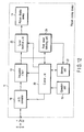
- FIG. 2 shows a signal processing system of the picture display apparatus 11. That is, in FIG. 2, reference numeral 17 denotes a video signal input terminal. In the video signal input terminal 17 is inputted an analog video signal in the form of an RGB signal or in the form of a YCbCr signal.
- the analog video signal inputted to the video signal input terminal 17 is supplied to an A/D converter 18, which converts the signal to a digital signal.
- the digital signal is integrated for a specified period by means of an integration circuit 19, and then supplied to the picture display device 14 and displayed on the display panel 14a.
- control unit 20 incorporates a central processing unit (CPU) and the like, which receives operation information from the operation unit 15 and controls respective units so as to reflect contents of the operation.
- CPU central processing unit
- the control unit utilizes a memory unit 21.
- the memory unit 21 mainly comprises a read only memory which stores a control program to be executed by the CPU of the control unit 20, a random access memory which provides the CPU with a work area, and a nonvolatile memory which stores various kinds of specified values, setting information, control information and the like.
- the control unit 20 outputs an integral range control signal indicating an integral range to the integration circuit 19, reads an integral value outputted from the integration circuit 19 in this integral range and executes offset adjustment and gain adjustment of the A/D converter 18 in accordance with the integral value.
- the A/D converter 18, the integration circuit 19 and the control unit 20 perform A/D conversion processing, integration processing and adjustment processing upon the R signal, G signal and B signal.
- the A/D converter 18, the integration circuit 19 and the control unit 20 perform A/D conversion processing, integration processing and adjustment processing upon the Y signal, Cb signal and Cr signal.
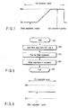
- FIG. 3 describes adjustments of offset and gain which are to be adjusted by the A/D converter 18. That is, comparison is made between a case where a signal conversion range when the A/D converter 18 converts an inputted analog video signal 22 to a digital signal has a gain A substantially corresponding to the amplitude of the analog video signal 22 and a case where it has gain B wider than the gain A.
- the case where it is set by the gain A provides a value 1.5 times the case where it is set by the gain B as for a digital signal produced by conversion to the same analog video signal 22.
- the maximum level portion 22a of the analog video signal 22 reaches a position lower by ⁇ than the maximum level Max of the signal conversion range, and the minimum level portion 22b of the analog video signal 22 reaches a position higher by ⁇ than the minimum level Min of the signal conversion range.
- gain adjustment of the A/D converter 18 is needed according to the amplitude of the inputted analog video signal 22.
- the central level namely, a central point of conversion to digital signals may be deflected by an amount corresponding to ⁇ depending on a situation as a gain B' indicated with a dotted line in the figure.
- offset by the amount corresponding to ⁇ is generated with respect to a central level portion 22c of the analog video signal 22.
- the offset adjustment of the A/D converter 18 is necessary according to the central level of the inputted analog video signal 22.
- a pedestal level after digitalization is preferred to be 80h. Accordingly, the offset adjustment is needed such that the pedestal level after the digitalization becomes 80h.
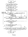
- FIG. 4 shows a flow chart of the offset adjustment operation.
- the analog video signal for offset adjustment is the RGB signal
- a minimum level Min (black) level is inputted.
- the analog video signal for offset adjustment is the YcbCr signal
- its central level is inputted. If the amplitude range after digitalization is 00h to FFh, the pedestal level after digitalization is 80h.
- step S3 the control unit 20 sets an integration range to the integration circuit 19, that is, a signal pickup range for reading an integration value from the integration circuit 19, and in step S4, the control unit 20 reads an integration value in the previously set integration range from the integration circuit 19.
- control unit 20 determines that the offset adjustment is completed in step S10, and terminates the processing (step S12).
- control unit 20 controls the A/D converter 18 to increment a current offset value with 1 in step S6.
- control unit 20 controls the A/D converter 18 to decrement a current offset value with 1 in step S7.
- control unit 20 corrects the offset value of the A/D converter 18 step by step such that the integration value becomes equal to the specified value.
- control unit 20 determines whether or not the number of times when the integration value is within a range of ⁇ 1 to the specified value exceeds a preliminarily set number of times (for example, 30 to 40). When it is determined that it does not exceed (NO), the procedure is returned to the processing of step S5.
- a preliminarily set number of times for example, 30 to 40.
- control unit 20 executes final determination to determine whether or not the integration value is within the range of ⁇ 1 to the specified value in the step S9.
- control unit 20 determines that the offset adjustment is completed in step S10, and terminates the processing (step S12). If it is determined that it is not within the range (NO), the control unit 20 determines that the offset adjustment is disabled in step S11, and terminates the processing (step S12).
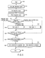
- FIG. 5 shows a flow chart of the gain adjustment operation.
- an analog video signal for gain adjustment is inputted to the A/D converter 18 through the video signal input terminal 17 in step S14.
- the analog video signal for gain adjustment is the RGB signal, and its maximum level Max (white level) is inputted.
- control unit 20 sets an integration range to the integration circuit 19, that is, a signal pickup range for reading out an integration value from the integration circuit 19 in step S15, and reads out an integration value in the previously set integration range from the integration circuit 19 in step S16.
- control unit 20 determines that the gain adjustment is completed in step S22, and terminates the processing (step S24).
- control unit 20 controls the A/D converter 18 to increment a current offset value with 1 in step S18.
- control unit 20 controls the A/D converter 18 to decrement the current offset value with 1 in step S19.
- control unit 20 corrects the gain value of the A/D converter 18 step by step such that the integration value becomes equal to the specified value.
- control unit 20 determines whether or not the number of times when the integration value is within a range of ⁇ 1 to the specified value exceeds a preliminarily set number of times (for example, 30 to 40). When it is determined that it does not exceed (NO), the procedure is returned to the processing of step S17.
- control unit 20 executes final determination to determine whether or not the integration value is within the range of ⁇ 1 to the specified value in the step S21.
- control unit 20 determines that the offset adjustment is completed in step S22, and terminates the processing (step S24). If it is determined that it is not within the range (NO), the control unit 20 determines that the offset adjustment is disabled in step S23, and terminates the processing (step S24).
- FIG. 6 shows a flow chart of an operation for automatically adjusting the offset and gain by inputting offset adjustment and gain adjustment analog RGB signals to the A/D converter 18.
- the adjustment analog RGB signal is inputted to the A/D converter 18 through the video signal input terminal 17 in step S26.
- a minimum level Min for offset adjustment and a maximum level Max for gain adjustment are mixed within a single horizontal period as shown in FIG. 7.
- control unit 20 sets an offset adjustment integration range in a portion of the minimum level Min of the inputted RGB signal and a gain adjustment integration range in a portion of the maximum level Max.
- control unit 20 executes the offset adjustment described in FIG. 4 on the offset adjustment integration range in step S27, and executes the gain adjustment described in FIG. 5 on the gain adjustment integration range in step S28.
- step S29 the control unit 20 readjusts the offset slightly deflected by the gain adjustment in step S28, determines that the automatic adjustment of the offset and gain is completed in step S30, and terminates the processing (step S31).
- the offset adjustment and gain adjustment if the offset adjustment is performed first and then they are executed alternately several times, a more reliable adjustment can be achieved.
- a result of the offset adjustment with the G signal in steps S27, S29 can be also applied to the Y signal. Further, a result of the gain adjustment with the RGB signal in step S28 can be also applied to the YCbCr signal.
- FIG. 8 shows a flow chart of an operation of automatically adjusting the offset by inputting the offset adjustment analog CbCr signal to the A/D converter 18.
- the analog CbCr signal needs to be a colorless flat signal, for example, a mono-chrome signal as shown in FIG. 9 for usage. Then, the control unit 20 sets an offset adjustment integration range at an arbitrary portion of the inputted CbCr signal.
- control unit 20 executes the offset adjustment described in FIG. 4 upon the offset adjustment integration range in step S34. Because the analog CbCr signal is used in this case, the specified value is a central level between the maximum level Max and the minimum level Min, that is, in case of 8 bits, 80h which is the central value of 00h to FFh. Thereafter, the control unit 20 confirms that the automatic adjustment of the offset is completed in step S35, and terminates the processing (step S36).
- FIG. 10 shows a flow chart of an operation of inputting the offset adjustment and gain adjustment analog RGB signals into the A/D converter 18 so as to automatically adjust the offset and gain, and subsequently, inputting the offset adjustment analog CbCr signal into the A/D converter 18 so as to automatically adjust the offset.
- step S37 the adjustment analog RGB signal is inputted to the A/D converter 18 through the video signal input terminal 17 in step S38.
- the control unit 20 executes the offset adjustment described in FIG. 4 on the offset adjustment integration range in step S39, and executes the gain adjustment described in FIG. 5 on the gain adjustment integration range in step S40.
- step S41 the control unit 20 readjusts the offset slightly deflected in the gain adjustment in step S40, and in step S42, the control unit 20 confirms that the automatic adjustment of the offset and gain is completed.
- step S43 the offset adjustment analog CbCr signal is inputted to the A/D converter 18 through the video signal input terminal 17 in step S43. Then, the control unit 20 executes the offset adjustment described in FIG. 4 upon the offset adjustment integration range in step S44. After that, the control unit 20 confirms that the automatic adjustment of the offset is completed in step S45, and terminates the processing (step S46).
- FIG. 11 shows a modification of the above-described embodiment.
- a cursor insertion unit 23 for displaying a cursor on the picture display device 14 under the control of the control unit 20 is disposed between the integration circuit 19 and the picture display device 14.
- an integrated range is displayed on the display panel 14a of the picture display device 14 during adjustment of the offset or gain.
- the user can determine whether or not the adjustment operation is being carried out properly because the integrated portion is displayed, thereby intensifying the reliability of adjustment.
- FIG. 12 shows further another modification of the above-described embodiment.
- this embodiment includes a peak value detecting unit 24 for detecting maximum and minimum peak values of a video signal from the output of the integration circuit 19.
- the specified value set in the memory unit 21 is changed such that the amplitude of the video signal is within the gain. Consequently, crush of a fine black detail or crush of a white portion of the video signal can be prevented.
- the present invention is not restricted to the above-described embodiment but may be embodied by modifying its components in various ways within a scope not departing from the gist of the invention.
- various aspects of the invention can be achieved. For example, it is permissible to delete some components from the entire components indicated in the embodiment. Moreover, it is permissible to combine components of different embodiments appropriately.
Landscapes
- Engineering & Computer Science (AREA)
- Theoretical Computer Science (AREA)
- Physics & Mathematics (AREA)
- Computer Hardware Design (AREA)
- General Physics & Mathematics (AREA)
- Picture Signal Circuits (AREA)
- Controls And Circuits For Display Device (AREA)
- Control Of Indicators Other Than Cathode Ray Tubes (AREA)
- Analogue/Digital Conversion (AREA)
Description
- The present invention relates to a video signal processing apparatus and a video signal processing method for displaying video signals on particularly a flat panel type display.
- As well known, in recent years, a flat panel type display using for example, a liquid crystal display panel, a plasma display panel or the like has been widely prevalent. As this kind of the flat panel type display, a picture projection type display or a projector also has tended to be prevail.
- In such a flat panel type display, after an analog video signal to be inputted in the form of an RGB signal or a YCbCr signal is digitized, the digitized signal is subjected to integral processing and supplied to the display panel, thereby displaying a picture.
- In this flat panel type display, it is necessary to implement offset adjustment and gain adjustment on an analog/digital (A/D) converter for digitizing an analog video signal in order to obtain optimal A/D conversion accuracy.
- Jpn. Pat. Appln. KOKAI Publication No. 5-243998 has disclosed a configuration for adjusting an A/D converter to obtain an optimal output when an offset adjustment reference voltage is inputted and for adjusting the A/C converter to obtain an optimal output when a gain adjustment reference voltage is inputted.
- However, the A/D conversion technology for digitizing the analog video signal is still on a development stage, so that development of a method more suitable for actual realization has been strongly demanded in several viewpoints as regards the offset and gain adjustments.
- US 5 087 973 discloses an image receiver control apparatus for performing clamp signal processing. The apparatus includes an analog clamper for clamping an input signal on a predetermined DC level, an A/D converter for A/C-converting an output from the analog clamper with a predetermined sample period of time, a timing signal generator, a central processing unit (CPU), a data selector for selecting one of a data signal output from the A/D converter and a data signal on a data bus connected to the CPU to supply the selected data signal to the RAM, and an address selector for selecting one of an address from the counter and an address on an address bus connected to the CPU to supply the selected address to the RAM.
- The data signals stored in the RAM are subjected to an operation by the CPU such that a noise reduction control signal in correspondence with a level of noise introduced during transfer or recording is determined by obtaining the variance of the data signals stored in said RAM and said noise reduction control signal is outputted from an output port of the CPU in correspondence with a noise level introduced during transfer or storing.
- The present invention has been accomplished in views of the above-described situations and an object of the invention is to provide a video signal processing apparatus and a video signal processing method capable of intensifying the efficiency of offset adjustment and gain adjustment upon the A/D converter and achieving high quality picture display.
- According to the present invention the above object is achieved by means of a video signal processing apparatus according to
claim 1, a video signal processing method according toclaim 7 and by a method for controlling the video signal processing apparatus as specified inclaim 11. The dependent claims are related to different advantageous aspects of the invention. - The invention can be more fully understood from the following detailed description when taken in conjunction with the accompanying drawings, in which:
- FIG. 1 is a front view for explaining an appearance of a picture display apparatus according to an embodiment of the present invention;
- FIG. 2 is a block diagram for explaining a signal processing system of the picture display apparatus according to the embodiment;
- FIG. 3 is a diagram for explaining adjustment of offset and gain of an A/D converter according to the embodiment;
- FIG. 4 is a flow chart for explaining the offset adjustment operation of the A/D converter according to the embodiment;
- FIG. 5 is a flow chart for explaining the gain adjustment operation of the A/D converter according to the embodiment;
- FIG. 6 is a flow chart for explaining the adjustment of offset and gain of the A/D converter with an RGB signal according to the embodiment;
- FIG. 7 is a diagram for explaining the RGB signal for use in the adjustment of offset and gain of the A/D converter according to the embodiment;
- FIG. 8 is a flow chart for explaining the offset adjustment operation of the A/D converter with a YCbCr signal according to the embodiment;
- FIG. 9 is a diagram for explaining the YCbCr signal for use in the offset adjustment operation of the A/D converter according to the embodiment;
- FIG. 10 is a flow chart for explaining that the adjustment of offset and gain of the A/D converter with the RGB signal and the adjustment of the offset with the YCbCr signal are carried out continuously;
- FIG. 11 is a block diagram for explaining a modification of the embodiment; and
- FIG. 12 is a block diagram for explaining another modification of the embodiment.
- Hereinafter, an embodiment of the present invention will be described in detail with reference to the accompanying drawings. FIG. 1 is a front view of a flat panel type
picture display apparatus 11 of this embodiment. - The
picture display apparatus 11 is mainly comprised of acabinet 12 and a supportingbase 13 for supporting thecabinet 12. In thecabinet 12, adisplay panel 14a of apicture display device 14, which will be described later, is disposed in the center of a front face thereof. - Further, in the
cabinet 12, anoperation unit 15 including apower switch 15a, areception unit 15b for receiving operation information sent from a wireless remote controller (not shown) and the like is disposed on both sides of thedisplay panel 14a. - On the other hand, the supporting
base 13 is coupled with the center of the bottom face of thecabinet 12 freely rotatably, and is configured to support thecabinet 12 in its standing position in a state in which it rests on apredetermined base 16 horizontally. - FIG. 2 shows a signal processing system of the
picture display apparatus 11. That is, in FIG. 2,reference numeral 17 denotes a video signal input terminal. In the videosignal input terminal 17 is inputted an analog video signal in the form of an RGB signal or in the form of a YCbCr signal. - The analog video signal inputted to the video
signal input terminal 17 is supplied to an A/D converter 18, which converts the signal to a digital signal. The digital signal is integrated for a specified period by means of anintegration circuit 19, and then supplied to thepicture display device 14 and displayed on thedisplay panel 14a. - Here, in the
picture display apparatus 11, its entire operation including the above-described display operation is totally controlled by acontrol unit 20. Thecontrol unit 20 incorporates a central processing unit (CPU) and the like, which receives operation information from theoperation unit 15 and controls respective units so as to reflect contents of the operation. - In this case, the control unit utilizes a
memory unit 21. That is, thememory unit 21 mainly comprises a read only memory which stores a control program to be executed by the CPU of thecontrol unit 20, a random access memory which provides the CPU with a work area, and a nonvolatile memory which stores various kinds of specified values, setting information, control information and the like. - The
control unit 20 outputs an integral range control signal indicating an integral range to theintegration circuit 19, reads an integral value outputted from theintegration circuit 19 in this integral range and executes offset adjustment and gain adjustment of the A/D converter 18 in accordance with the integral value. - When the inputted analog video signal is the RGB signal, the A/
D converter 18, theintegration circuit 19 and thecontrol unit 20 perform A/D conversion processing, integration processing and adjustment processing upon the R signal, G signal and B signal. When the inputted analog video signal is the YCbCr signal, the A/D converter 18, theintegration circuit 19 and thecontrol unit 20 perform A/D conversion processing, integration processing and adjustment processing upon the Y signal, Cb signal and Cr signal. - FIG. 3 describes adjustments of offset and gain which are to be adjusted by the A/
D converter 18. That is, comparison is made between a case where a signal conversion range when the A/D converter 18 converts an inputtedanalog video signal 22 to a digital signal has a gain A substantially corresponding to the amplitude of theanalog video signal 22 and a case where it has gain B wider than the gain A. - Assuming that the gain A is 2/3 times the gain B in this case, the case where it is set by the gain A provides a value 1.5 times the case where it is set by the gain B as for a digital signal produced by conversion to the same
analog video signal 22. - That is, assume that respective central levels of the gain A, gain B and
analog video signal 22 coincide at a position indicated by a dot and dash line in FIG. 3. In the case of the gain A, amaximum level portion 22a of theanalog video signal 22 reaches substantially near the maximum level Max of the signal conversion range, and aminimum level portion 22b of theanalog video signal 22 reaches substantially near the minimum level Min of the signal conversion range. - Contrary to this, in the case of the gain B, the
maximum level portion 22a of theanalog video signal 22 reaches a position lower by α than the maximum level Max of the signal conversion range, and theminimum level portion 22b of theanalog video signal 22 reaches a position higher by α than the minimum level Min of the signal conversion range. - As a result, gain adjustment of the A/
D converter 18 is needed according to the amplitude of the inputtedanalog video signal 22. - Even if the same gain width as the gain B indicated with a solid line is provided, the central level, namely, a central point of conversion to digital signals may be deflected by an amount corresponding to β depending on a situation as a gain B' indicated with a dotted line in the figure. In this case, as compared with the case of the gain B, offset by the amount corresponding to β is generated with respect to a
central level portion 22c of theanalog video signal 22. - Thus, the offset adjustment of the A/
D converter 18 is necessary according to the central level of the inputtedanalog video signal 22. For the YCbCr signal to be inputted, a pedestal level after digitalization is preferred to be 80h. Accordingly, the offset adjustment is needed such that the pedestal level after the digitalization becomes 80h. - FIG. 4 shows a flow chart of the offset adjustment operation. First, after the processing is started (step S1), an analog video signal for offset adjustment is inputted to the A/
D converter 18 through the videosignal input terminal 17 in step S2. - Here, when the analog video signal for offset adjustment is the RGB signal, a minimum level Min (black) level is inputted. In addition, when the analog video signal for offset adjustment is the YcbCr signal, its central level is inputted. If the amplitude range after digitalization is 00h to FFh, the pedestal level after digitalization is 80h.
- Then, in step S3, the
control unit 20 sets an integration range to theintegration circuit 19, that is, a signal pickup range for reading an integration value from theintegration circuit 19, and in step S4, thecontrol unit 20 reads an integration value in the previously set integration range from theintegration circuit 19. - Thereafter, in step S5, the
control unit 20 compares the integration value read out from theintegration circuit 19 with the specified value preliminarily set in thememory unit 21, and determines which state is established from among the following three states, "integration value = specified value", "integration value < specified value" and "integration value > specified value". - If it is determined that "integration value = specified value" is established, the
control unit 20 determines that the offset adjustment is completed in step S10, and terminates the processing (step S12). - If it is determined that "integration value < specified value" is established in the step S5, the
control unit 20 controls the A/D converter 18 to increment a current offset value with 1 in step S6. - On the other hand, if it is determined that "integration value > specified value" is established in the step S5, the
control unit 20 controls the A/D converter 18 to decrement a current offset value with 1 in step S7. - That is, the
control unit 20 corrects the offset value of the A/D converter 18 step by step such that the integration value becomes equal to the specified value. - After the step S6 or S7, the
control unit 20 determines whether or not the number of times when the integration value is within a range of ±1 to the specified value exceeds a preliminarily set number of times (for example, 30 to 40). When it is determined that it does not exceed (NO), the procedure is returned to the processing of step S5. - If it is determined that the number of times when the integration value is within the range of ±1 to the specified value exceeds the preliminarily set number of times (YES) in the step S8, the
control unit 20 executes final determination to determine whether or not the integration value is within the range of ±1 to the specified value in the step S9. - If it is determined that it is within the range (YES), the
control unit 20 determines that the offset adjustment is completed in step S10, and terminates the processing (step S12). If it is determined that it is not within the range (NO), thecontrol unit 20 determines that the offset adjustment is disabled in step S11, and terminates the processing (step S12). - FIG. 5 shows a flow chart of the gain adjustment operation. After the processing is started (step S13), an analog video signal for gain adjustment is inputted to the A/
D converter 18 through the videosignal input terminal 17 in step S14. In this case, the analog video signal for gain adjustment is the RGB signal, and its maximum level Max (white level) is inputted. - Then, the
control unit 20 sets an integration range to theintegration circuit 19, that is, a signal pickup range for reading out an integration value from theintegration circuit 19 in step S15, and reads out an integration value in the previously set integration range from theintegration circuit 19 in step S16. - Thereafter, the
control unit 20 compares the integration value read from theintegration circuit 19 with the specified value set in thememory unit 21, and determines which state is established from among the following three states, "integration value = specified value", "integration value < specified value" and "integration value > specified value". - If it is determined that "integration value = specified value" is established, the
control unit 20 determines that the gain adjustment is completed in step S22, and terminates the processing (step S24). - If it is determined that "integration value < specified value" is established in the step S17, the
control unit 20 controls the A/D converter 18 to increment a current offset value with 1 in step S18. - On the other hand, if it is determined that "integration value > specified value" is established in the step S17, the
control unit 20 controls the A/D converter 18 to decrement the current offset value with 1 in step S19. - That is, the
control unit 20 corrects the gain value of the A/D converter 18 step by step such that the integration value becomes equal to the specified value. - After the step S18 or S19, the
control unit 20 determines whether or not the number of times when the integration value is within a range of ±1 to the specified value exceeds a preliminarily set number of times (for example, 30 to 40). When it is determined that it does not exceed (NO), the procedure is returned to the processing of step S17. - If it is determined that the number of times when the integration value is within the range of ±1 to the specified value exceeds the preliminarily set number of times (YES) in the step S20, the
control unit 20 executes final determination to determine whether or not the integration value is within the range of ±1 to the specified value in the step S21. - If it is determined that it is within the range (YES), the
control unit 20 determines that the offset adjustment is completed in step S22, and terminates the processing (step S24). If it is determined that it is not within the range (NO), thecontrol unit 20 determines that the offset adjustment is disabled in step S23, and terminates the processing (step S24). - According to the above-mentioned embodiment, even if an integration value obtained by inputting offset adjustment and gain adjustment analog video signals to the A/
D converter 18 does not coincide with a preliminarily set specified value, if it is within the allowance range obtained by incrementing/decrementing the specified value with 1 at a predetermined number of times or more, it is determined that the adjustment is completed. Consequently, the efficiency of the offset adjustment and gain adjustment to the A/D converter 18 can be intensified. - FIG. 6 shows a flow chart of an operation for automatically adjusting the offset and gain by inputting offset adjustment and gain adjustment analog RGB signals to the A/
D converter 18. - First, after the processing is started (step S25), the adjustment analog RGB signal is inputted to the A/
D converter 18 through the videosignal input terminal 17 in step S26. In the adjustment analog RGB signal, a minimum level Min for offset adjustment and a maximum level Max for gain adjustment are mixed within a single horizontal period as shown in FIG. 7. - In this case, the
control unit 20 sets an offset adjustment integration range in a portion of the minimum level Min of the inputted RGB signal and a gain adjustment integration range in a portion of the maximum level Max. - As a consequence, the
control unit 20 executes the offset adjustment described in FIG. 4 on the offset adjustment integration range in step S27, and executes the gain adjustment described in FIG. 5 on the gain adjustment integration range in step S28. - In step S29, the
control unit 20 readjusts the offset slightly deflected by the gain adjustment in step S28, determines that the automatic adjustment of the offset and gain is completed in step S30, and terminates the processing (step S31). - As for the offset adjustment and gain adjustment, if the offset adjustment is performed first and then they are executed alternately several times, a more reliable adjustment can be achieved.
- A result of the offset adjustment with the G signal in steps S27, S29 can be also applied to the Y signal. Further, a result of the gain adjustment with the RGB signal in step S28 can be also applied to the YCbCr signal.
- FIG. 8 shows a flow chart of an operation of automatically adjusting the offset by inputting the offset adjustment analog CbCr signal to the A/
D converter 18. First, after the processing is started (step S32), the offset adjustment analog CbCr signal is inputted to the A/D converter 18 through the videosignal input terminal 17 in step S33. - The analog CbCr signal needs to be a colorless flat signal, for example, a mono-chrome signal as shown in FIG. 9 for usage. Then, the
control unit 20 sets an offset adjustment integration range at an arbitrary portion of the inputted CbCr signal. - Then, the
control unit 20 executes the offset adjustment described in FIG. 4 upon the offset adjustment integration range in step S34. Because the analog CbCr signal is used in this case, the specified value is a central level between the maximum level Max and the minimum level Min, that is, in case of 8 bits, 80h which is the central value of 00h to FFh. Thereafter, thecontrol unit 20 confirms that the automatic adjustment of the offset is completed in step S35, and terminates the processing (step S36). - FIG. 10 shows a flow chart of an operation of inputting the offset adjustment and gain adjustment analog RGB signals into the A/
D converter 18 so as to automatically adjust the offset and gain, and subsequently, inputting the offset adjustment analog CbCr signal into the A/D converter 18 so as to automatically adjust the offset. - That is, after the processing is started (step S37), the adjustment analog RGB signal is inputted to the A/
D converter 18 through the videosignal input terminal 17 in step S38. Then, thecontrol unit 20 executes the offset adjustment described in FIG. 4 on the offset adjustment integration range in step S39, and executes the gain adjustment described in FIG. 5 on the gain adjustment integration range in step S40. - Then, in step S41, the
control unit 20 readjusts the offset slightly deflected in the gain adjustment in step S40, and in step S42, thecontrol unit 20 confirms that the automatic adjustment of the offset and gain is completed. - Thereafter, the offset adjustment analog CbCr signal is inputted to the A/
D converter 18 through the videosignal input terminal 17 in step S43. Then, thecontrol unit 20 executes the offset adjustment described in FIG. 4 upon the offset adjustment integration range in step S44. After that, thecontrol unit 20 confirms that the automatic adjustment of the offset is completed in step S45, and terminates the processing (step S46). - FIG. 11 shows a modification of the above-described embodiment. Explaining by attaching like reference numerals to the same components as in FIG. 2, a
cursor insertion unit 23 for displaying a cursor on thepicture display device 14 under the control of thecontrol unit 20 is disposed between theintegration circuit 19 and thepicture display device 14. - If a signal obtained by processing a video signal within the integration range of the
integration circuit 19 to a specified level is used as a cursor, an integrated range is displayed on thedisplay panel 14a of thepicture display device 14 during adjustment of the offset or gain. Thus, the user can determine whether or not the adjustment operation is being carried out properly because the integrated portion is displayed, thereby intensifying the reliability of adjustment. - FIG. 12 shows further another modification of the above-described embodiment. Explaining by attaching like reference numerals to the same components as in FIG. 11, in FIG. 12, this embodiment includes a peak
value detecting unit 24 for detecting maximum and minimum peak values of a video signal from the output of theintegration circuit 19. - When, as a result of detection result of the peak
value detecting unit 24, a detected video signal has a level higher than currently set gain, the specified value set in thememory unit 21 is changed such that the amplitude of the video signal is within the gain. Consequently, crush of a fine black detail or crush of a white portion of the video signal can be prevented. - In the meantime, the present invention is not restricted to the above-described embodiment but may be embodied by modifying its components in various ways within a scope not departing from the gist of the invention. In addition, by combining plural components disclosed in the above-described embodiment appropriately, various aspects of the invention can be achieved. For example, it is permissible to delete some components from the entire components indicated in the embodiment. Moreover, it is permissible to combine components of different embodiments appropriately.
Claims (11)
- A video signal processing apparatus comprising:an A/D converting unit (18) configured to digitize an inputted analog video signal;an integration unit (19) configured to integrate the video signals digitized by the A/D converting unit (18) within a predetermined integration range;a picture display unit (14) configured to display a picture based on an output signal of the integration unit (19) ;an offset adjusting unit (20) having:a first detecting unit (20) configured to, when an analog video signal to be inputted to the A/D converting unit (18) is an offset adjustment signal of the A/D converting unit (18), detect a difference between an integration value obtained by the integration unit (19) and a first specified value that is preliminarily set;a first correcting unit (20) configured to, when the difference is detected by the first detecting unit (20), correct an offset value of the A/D converting unit (18) such that the integration value is equal to the first specified value; anda first determining unit configured to determine whether or not the offset adjustment is completed based on the number of times when the offset value corrected by the first correcting unit (20) is within a range defined by adding a predetermined error to the first specified value; anda gain adjusting unit (20) having:a second detecting unit (20) configured to, when the analog video signal to be inputted to the A/D converting unit (18) is a gain adjustment signal of the A/D converting unit (18), detect a difference between the integration value obtained by the integration unit (19) and a second specified value that is preliminarily set;a second correcting unit (20) configured to, when the difference is detected by the second detecting unit (20), correct the gain value of the A/D converting unit (18) such that the integration value is equal to the second specified value; anda second determining unit (20) configured to determine whether or not the gain adjustment is completed based on the number of times when the gain value corrected by the second correcting unit (20) is within a range defined by adding a predetermined error to the second specified value.
- A video signal processing apparatus according to claim 1, wherein the offset adjustment signal of the A/D converting unit (18) is a black level analog RGB signal or a colorless CbCr signal.
- A video signal processing apparatus according to claim 1, wherein the gain adjustment signal of the A/D converting unit (18) is a white level analog RGB signal.
- A video signal processing apparatus according to claim 1, further comprising:a peak detecting unit (24) configured to detect a peak level of the output signal of the integration unit (19) ; anda changing unit (20) configured to, when the peak level detected by the peak detecting unit (24) exceeds a range of a gain set in the A/D converting unit (18), change the specified value such that all the output signals of the integration unit (19) are within the gain of the A/D converting unit (18).
- A video signal processing apparatus according to claim 1, further comprising a cursor generating unit (23) configured to generate a cursor displayed on the picture display unit (14) based on an output signal within a predetermined integration range of the integration unit (19), wherein an integration range under adjustment is displayed with the cursor.
- A video signal processing apparatus according to claim 1, wherein the offset adjustment operation by the offset adjusting unit (20) and the gain adjustment operation by the gain adjusting unit (20) are carried out alternately and repeatedly.
- A video signal processing method comprising:a first step of digitizing an inputted analog video signal by an A/D converting unit (18);a second step of integrating the digitized video signal by an integration unit (19) within a predetermined integration range;a third step of displaying a picture by a picture display unit (14) based on an output signal of the integration unit (19);a fourth step (S5, S17) of, when an analog video signal to be inputted to the A/D converting unit (18) is an adjustment signal of the A/D converting unit (18), detecting a difference between an integration value obtained by the integration unit (19) and a preliminarily set specified value;a fifth step (S6, S7, S18, S19) of, when the difference is detected, correcting an adjusted value of the A/D converting unit (18) such that the integration value is equal to the specified value; anda sixth step (S8 to S11, S20 to S23) of determining whether or nor the adjustment is completed based on the number of times when the adjusted value corrected by the correcting unit is within a range defined by adding a predetermined error to the specified value.
- A video signal processing method according to claim 7, wherein
when the analog video signal to be inputted to the A/D converting unit (18) is an offset adjustment signal of the A/D converting unit (18), the fourth step (S5) detects a difference between an integration value obtained by the integration unit (19) and a preliminarily set specified value,
when the difference is detected by the fourth step (S5), the fifth step (S6, S7) corrects an offset value of the A/D converting unit (18) such that the integration value is equal to the specified value, and
the sixth step (S8 to S11) determines whether or nor the offset adjustment is completed based on the number of times when the offset value corrected in the fifth step (S6, S7) is within a range defined by adding a predetermined error to the specified value. - A video signal processing method according to claim 7, wherein
when the analog video signal to be inputted to the A/D converting unit (18) is a gain adjustment signal of the A/D converting unit (18), the fourth step (S17) detects a difference between an integration value obtained by the integration unit (19) and a preliminarily set specified value,
when the difference is detected by the fourth step (S17), the fifth step (S18, S19) corrects a gain value of the A/D converting unit (18) such that the integration value is equal to the specified value, and
the sixth step (S20 to S23) determines whether or not the gain adjustment is completed based on the number of times when the gain value corrected in the fifth step (S18, S19) is within a range defined by adding a predetermined error to the specified value. - A method of controlling the video signal processing apparatus according to claim 1, comprising:a first step (S27) of executing the offset adjustment operation by the offset adjusting unit (20); anda second step (S28, S29) of, after the first step (S27), executing the gain adjustment operation by the gain adjusting unit (20) and the offset adjustment operation by the offset adjusting unit (20) alternately and repeatedly.
- A method of controlling the video signal processing apparatus according to claim 1, comprising:a first step (S39) in which the offset adjusting unit (20) carries out the offset adjustment operation by using an RGB signal as an offset adjustment signal;a second step (S40) in which, after the first step (S39), the gain adjusting unit (20) carries out the gain adjustment operation by using an RGB signal as a gain adjustment signal; anda third step (S44) in which, after the second step (S40), the offset adjusting unit (20) carries out the offset adjustment operation by using a CbCr signal as an offset adjustment signal.
Applications Claiming Priority (2)
| Application Number | Priority Date | Filing Date | Title |
|---|---|---|---|
| JP2004178482 | 2004-06-16 | ||
| JP2004178482A JP2006005559A (en) | 2004-06-16 | 2004-06-16 | Video signal processing apparatus and video signal processing method |
Publications (2)
| Publication Number | Publication Date |
|---|---|
| EP1608150A1 EP1608150A1 (en) | 2005-12-21 |
| EP1608150B1 true EP1608150B1 (en) | 2007-01-24 |
Family
ID=34939918
Family Applications (1)
| Application Number | Title | Priority Date | Filing Date |
|---|---|---|---|
| EP05104305A Expired - Lifetime EP1608150B1 (en) | 2004-06-16 | 2005-05-20 | Video signal processing apparatus and video signal processing method |
Country Status (5)
| Country | Link |
|---|---|
| US (1) | US7265695B2 (en) |
| EP (1) | EP1608150B1 (en) |
| JP (1) | JP2006005559A (en) |
| CN (1) | CN1713250A (en) |
| DE (1) | DE602005000490T2 (en) |
Families Citing this family (3)
| Publication number | Priority date | Publication date | Assignee | Title |
|---|---|---|---|---|
| JP5147219B2 (en) * | 2006-11-16 | 2013-02-20 | 三菱電機株式会社 | Automatic image adjustment system |
| JP5427911B2 (en) * | 2012-04-11 | 2014-02-26 | Eizo株式会社 | Cursor movement control method, computer program, cursor movement control device, and image display system |
| CN115314045B (en) * | 2022-10-08 | 2023-01-20 | 深圳市好盈科技股份有限公司 | Method, system, device and medium for adaptive calibration of finger-dialing output interval |
Family Cites Families (9)
| Publication number | Priority date | Publication date | Assignee | Title |
|---|---|---|---|---|
| US4053946A (en) * | 1975-11-24 | 1977-10-11 | Hughes Aircraft Company | Modular programmable digital scan converter |
| US4517586A (en) * | 1982-11-23 | 1985-05-14 | Rca Corporation | Digital television receiver with analog-to-digital converter having time multiplexed gain |
| GB8521019D0 (en) * | 1985-08-22 | 1986-10-01 | Rank Pullin Controls Ltd | Imaging apparatus |
| WO1990006035A1 (en) * | 1988-11-17 | 1990-05-31 | Matsushita Electric Industrial Co., Ltd. | Picture receiver controller |
| JPH0449780A (en) * | 1990-06-18 | 1992-02-19 | Victor Co Of Japan Ltd | Video signal clamping circuit |
| JPH05243998A (en) * | 1992-02-27 | 1993-09-21 | Fuji Facom Corp | Automatic adjusting device for analog/digital converter system |
| JPH11219154A (en) | 1998-02-04 | 1999-08-10 | Sharp Corp | Video signal level adjusting device and video signal level adjusting method |
| TW559699B (en) * | 2000-01-12 | 2003-11-01 | Sony Corp | Image display device and method |
| US7034722B2 (en) * | 2004-07-29 | 2006-04-25 | Genesis Microchip Inc. | ADC calibration to accommodate temperature variation using vertical blanking interrupts |
-
2004
- 2004-06-16 JP JP2004178482A patent/JP2006005559A/en not_active Withdrawn
-
2005
- 2005-05-20 DE DE602005000490T patent/DE602005000490T2/en not_active Expired - Fee Related
- 2005-05-20 EP EP05104305A patent/EP1608150B1/en not_active Expired - Lifetime
- 2005-06-10 US US11/149,187 patent/US7265695B2/en not_active Expired - Fee Related
- 2005-06-16 CN CNA2005100789189A patent/CN1713250A/en active Pending
Also Published As
| Publication number | Publication date |
|---|---|
| EP1608150A1 (en) | 2005-12-21 |
| DE602005000490T2 (en) | 2007-10-31 |
| US7265695B2 (en) | 2007-09-04 |
| CN1713250A (en) | 2005-12-28 |
| JP2006005559A (en) | 2006-01-05 |
| DE602005000490D1 (en) | 2007-03-15 |
| US20050280642A1 (en) | 2005-12-22 |
Similar Documents
| Publication | Publication Date | Title |
|---|---|---|
| US7551196B2 (en) | Endoscope apparatus | |
| US6597390B1 (en) | Electronic endoscope apparatus | |
| US20050012868A1 (en) | Analog-to-digital converting apparatus for processing a plurality of analog input signals at high rate and display device using the same | |
| EP0782331B1 (en) | Multiple video input clamping arrangement | |
| KR890005235B1 (en) | A / D converter | |
| US7324164B2 (en) | Display apparatus and control method thereof | |
| CN88100873A (en) | Synchronization system for semi-digital signals | |
| KR0147862B1 (en) | Beam current controlling circuit for multi-mode monitor and method thereof | |
| EP1608150A1 (en) | Video signal processing apparatus and video signal processing method | |
| US6128048A (en) | Convergence correction apparatus for projection television and method thereof | |
| JP2005250113A (en) | Display device and adjustment method | |
| JP3250676B2 (en) | Imaging device | |
| EP1071281B1 (en) | Automatic luminance adjustment device and method | |
| KR100308259B1 (en) | Digital convergence compensator | |
| EP1734495B1 (en) | Picture signal processing device | |
| KR100492120B1 (en) | Photographing apparatus having function of back light compensation and control method thereof | |
| JPH07231409A (en) | Self-calibration circuit | |
| JP3451216B2 (en) | Image display device and sampling frequency adjustment method | |
| JP3252977B2 (en) | Imaging device | |
| JP3139471B2 (en) | Multi-scan display | |
| KR0164967B1 (en) | Apparatus and method for automatically controlling horizontal synchronization position in r.g.b mode | |
| KR970008371B1 (en) | Television receiver | |
| US6683586B2 (en) | Apparatus and method of adjusting horizontal position for a video display appliance | |
| JP3228142B2 (en) | Display device | |
| JPH1065980A (en) | Television receiver |
Legal Events
| Date | Code | Title | Description |
|---|---|---|---|
| PUAI | Public reference made under article 153(3) epc to a published international application that has entered the european phase |
Free format text: ORIGINAL CODE: 0009012 |
|
| 17P | Request for examination filed |
Effective date: 20050523 |
|
| AK | Designated contracting states |
Kind code of ref document: A1 Designated state(s): AT BE BG CH CY CZ DE DK EE ES FI FR GB GR HU IE IS IT LI LT LU MC NL PL PT RO SE SI SK TR |
|
| AX | Request for extension of the european patent |
Extension state: AL BA HR LV MK YU |
|
| GRAP | Despatch of communication of intention to grant a patent |
Free format text: ORIGINAL CODE: EPIDOSNIGR1 |
|
| AKX | Designation fees paid |
Designated state(s): DE FR GB |
|
| GRAS | Grant fee paid |
Free format text: ORIGINAL CODE: EPIDOSNIGR3 |
|
| GRAA | (expected) grant |
Free format text: ORIGINAL CODE: 0009210 |
|
| AK | Designated contracting states |
Kind code of ref document: B1 Designated state(s): DE FR GB |
|
| REG | Reference to a national code |
Ref country code: GB Ref legal event code: FG4D |
|
| REF | Corresponds to: |
Ref document number: 602005000490 Country of ref document: DE Date of ref document: 20070315 Kind code of ref document: P |
|
| ET | Fr: translation filed | ||
| PLBE | No opposition filed within time limit |
Free format text: ORIGINAL CODE: 0009261 |
|
| STAA | Information on the status of an ep patent application or granted ep patent |
Free format text: STATUS: NO OPPOSITION FILED WITHIN TIME LIMIT |
|
| 26N | No opposition filed |
Effective date: 20071025 |
|
| PGFP | Annual fee paid to national office [announced via postgrant information from national office to epo] |
Ref country code: DE Payment date: 20080529 Year of fee payment: 4 |
|
| GBPC | Gb: european patent ceased through non-payment of renewal fee |
Effective date: 20090520 |
|
| REG | Reference to a national code |
Ref country code: FR Ref legal event code: ST Effective date: 20100129 |
|
| PG25 | Lapsed in a contracting state [announced via postgrant information from national office to epo] |
Ref country code: FR Free format text: LAPSE BECAUSE OF NON-PAYMENT OF DUE FEES Effective date: 20090602 |
|
| PGFP | Annual fee paid to national office [announced via postgrant information from national office to epo] |
Ref country code: FR Payment date: 20080514 Year of fee payment: 4 |
|
| PG25 | Lapsed in a contracting state [announced via postgrant information from national office to epo] |
Ref country code: GB Free format text: LAPSE BECAUSE OF NON-PAYMENT OF DUE FEES Effective date: 20090520 |
|
| PG25 | Lapsed in a contracting state [announced via postgrant information from national office to epo] |
Ref country code: DE Free format text: LAPSE BECAUSE OF NON-PAYMENT OF DUE FEES Effective date: 20091201 |