EP1607932A1 - Organic light emitting display and control method thereof - Google Patents

Organic light emitting display and control method thereof Download PDF

Info

Publication number
EP1607932A1
EP1607932A1 EP05104919A EP05104919A EP1607932A1 EP 1607932 A1 EP1607932 A1 EP 1607932A1 EP 05104919 A EP05104919 A EP 05104919A EP 05104919 A EP05104919 A EP 05104919A EP 1607932 A1 EP1607932 A1 EP 1607932A1
Authority
EP
European Patent Office
Prior art keywords
gamma correction
signal
light emitting
organic light
emitting display
Prior art date
Legal status (The legal status is an assumption and is not a legal conclusion. Google has not performed a legal analysis and makes no representation as to the accuracy of the status listed.)
Withdrawn
Application number
EP05104919A
Other languages
German (de)
French (fr)
Inventor
Jae Sung Doosan Apt. 103-102 3-Ga Lee
Current Assignee (The listed assignees may be inaccurate. Google has not performed a legal analysis and makes no representation or warranty as to the accuracy of the list.)
Samsung Display Co Ltd
Original Assignee
Samsung SDI Co Ltd
Priority date (The priority date is an assumption and is not a legal conclusion. Google has not performed a legal analysis and makes no representation as to the accuracy of the date listed.)
Filing date
Publication date
Application filed by Samsung SDI Co Ltd filed Critical Samsung SDI Co Ltd
Publication of EP1607932A1 publication Critical patent/EP1607932A1/en
Withdrawn legal-status Critical Current

Links

Images

Classifications

    • GPHYSICS
    • G09EDUCATION; CRYPTOGRAPHY; DISPLAY; ADVERTISING; SEALS
    • G09GARRANGEMENTS OR CIRCUITS FOR CONTROL OF INDICATING DEVICES USING STATIC MEANS TO PRESENT VARIABLE INFORMATION
    • G09G3/00Control arrangements or circuits, of interest only in connection with visual indicators other than cathode-ray tubes
    • G09G3/20Control arrangements or circuits, of interest only in connection with visual indicators other than cathode-ray tubes for presentation of an assembly of a number of characters, e.g. a page, by composing the assembly by combination of individual elements arranged in a matrix no fixed position being assigned to or needed to be assigned to the individual characters or partial characters
    • G09G3/22Control arrangements or circuits, of interest only in connection with visual indicators other than cathode-ray tubes for presentation of an assembly of a number of characters, e.g. a page, by composing the assembly by combination of individual elements arranged in a matrix no fixed position being assigned to or needed to be assigned to the individual characters or partial characters using controlled light sources
    • G09G3/30Control arrangements or circuits, of interest only in connection with visual indicators other than cathode-ray tubes for presentation of an assembly of a number of characters, e.g. a page, by composing the assembly by combination of individual elements arranged in a matrix no fixed position being assigned to or needed to be assigned to the individual characters or partial characters using controlled light sources using electroluminescent panels
    • GPHYSICS
    • G09EDUCATION; CRYPTOGRAPHY; DISPLAY; ADVERTISING; SEALS
    • G09GARRANGEMENTS OR CIRCUITS FOR CONTROL OF INDICATING DEVICES USING STATIC MEANS TO PRESENT VARIABLE INFORMATION
    • G09G3/00Control arrangements or circuits, of interest only in connection with visual indicators other than cathode-ray tubes
    • G09G3/20Control arrangements or circuits, of interest only in connection with visual indicators other than cathode-ray tubes for presentation of an assembly of a number of characters, e.g. a page, by composing the assembly by combination of individual elements arranged in a matrix no fixed position being assigned to or needed to be assigned to the individual characters or partial characters
    • G09G3/22Control arrangements or circuits, of interest only in connection with visual indicators other than cathode-ray tubes for presentation of an assembly of a number of characters, e.g. a page, by composing the assembly by combination of individual elements arranged in a matrix no fixed position being assigned to or needed to be assigned to the individual characters or partial characters using controlled light sources
    • G09G3/30Control arrangements or circuits, of interest only in connection with visual indicators other than cathode-ray tubes for presentation of an assembly of a number of characters, e.g. a page, by composing the assembly by combination of individual elements arranged in a matrix no fixed position being assigned to or needed to be assigned to the individual characters or partial characters using controlled light sources using electroluminescent panels
    • G09G3/32Control arrangements or circuits, of interest only in connection with visual indicators other than cathode-ray tubes for presentation of an assembly of a number of characters, e.g. a page, by composing the assembly by combination of individual elements arranged in a matrix no fixed position being assigned to or needed to be assigned to the individual characters or partial characters using controlled light sources using electroluminescent panels semiconductive, e.g. using light-emitting diodes [LED]
    • G09G3/3208Control arrangements or circuits, of interest only in connection with visual indicators other than cathode-ray tubes for presentation of an assembly of a number of characters, e.g. a page, by composing the assembly by combination of individual elements arranged in a matrix no fixed position being assigned to or needed to be assigned to the individual characters or partial characters using controlled light sources using electroluminescent panels semiconductive, e.g. using light-emitting diodes [LED] organic, e.g. using organic light-emitting diodes [OLED]
    • G09G3/3225Control arrangements or circuits, of interest only in connection with visual indicators other than cathode-ray tubes for presentation of an assembly of a number of characters, e.g. a page, by composing the assembly by combination of individual elements arranged in a matrix no fixed position being assigned to or needed to be assigned to the individual characters or partial characters using controlled light sources using electroluminescent panels semiconductive, e.g. using light-emitting diodes [LED] organic, e.g. using organic light-emitting diodes [OLED] using an active matrix
    • G09G3/3233Control arrangements or circuits, of interest only in connection with visual indicators other than cathode-ray tubes for presentation of an assembly of a number of characters, e.g. a page, by composing the assembly by combination of individual elements arranged in a matrix no fixed position being assigned to or needed to be assigned to the individual characters or partial characters using controlled light sources using electroluminescent panels semiconductive, e.g. using light-emitting diodes [LED] organic, e.g. using organic light-emitting diodes [OLED] using an active matrix with pixel circuitry controlling the current through the light-emitting element
    • GPHYSICS
    • G09EDUCATION; CRYPTOGRAPHY; DISPLAY; ADVERTISING; SEALS
    • G09GARRANGEMENTS OR CIRCUITS FOR CONTROL OF INDICATING DEVICES USING STATIC MEANS TO PRESENT VARIABLE INFORMATION
    • G09G2300/00Aspects of the constitution of display devices
    • G09G2300/08Active matrix structure, i.e. with use of active elements, inclusive of non-linear two terminal elements, in the pixels together with light emitting or modulating elements
    • G09G2300/0809Several active elements per pixel in active matrix panels
    • G09G2300/0842Several active elements per pixel in active matrix panels forming a memory circuit, e.g. a dynamic memory with one capacitor
    • GPHYSICS
    • G09EDUCATION; CRYPTOGRAPHY; DISPLAY; ADVERTISING; SEALS
    • G09GARRANGEMENTS OR CIRCUITS FOR CONTROL OF INDICATING DEVICES USING STATIC MEANS TO PRESENT VARIABLE INFORMATION
    • G09G2310/00Command of the display device
    • G09G2310/02Addressing, scanning or driving the display screen or processing steps related thereto
    • G09G2310/0264Details of driving circuits
    • G09G2310/027Details of drivers for data electrodes, the drivers handling digital grey scale data, e.g. use of D/A converters
    • GPHYSICS
    • G09EDUCATION; CRYPTOGRAPHY; DISPLAY; ADVERTISING; SEALS
    • G09GARRANGEMENTS OR CIRCUITS FOR CONTROL OF INDICATING DEVICES USING STATIC MEANS TO PRESENT VARIABLE INFORMATION
    • G09G2320/00Control of display operating conditions
    • G09G2320/06Adjustment of display parameters
    • G09G2320/0626Adjustment of display parameters for control of overall brightness
    • GPHYSICS
    • G09EDUCATION; CRYPTOGRAPHY; DISPLAY; ADVERTISING; SEALS
    • G09GARRANGEMENTS OR CIRCUITS FOR CONTROL OF INDICATING DEVICES USING STATIC MEANS TO PRESENT VARIABLE INFORMATION
    • G09G2320/00Control of display operating conditions
    • G09G2320/06Adjustment of display parameters
    • G09G2320/0673Adjustment of display parameters for control of gamma adjustment, e.g. selecting another gamma curve
    • GPHYSICS
    • G09EDUCATION; CRYPTOGRAPHY; DISPLAY; ADVERTISING; SEALS
    • G09GARRANGEMENTS OR CIRCUITS FOR CONTROL OF INDICATING DEVICES USING STATIC MEANS TO PRESENT VARIABLE INFORMATION
    • G09G2330/00Aspects of power supply; Aspects of display protection and defect management
    • G09G2330/02Details of power systems and of start or stop of display operation
    • G09G2330/021Power management, e.g. power saving
    • GPHYSICS
    • G09EDUCATION; CRYPTOGRAPHY; DISPLAY; ADVERTISING; SEALS
    • G09GARRANGEMENTS OR CIRCUITS FOR CONTROL OF INDICATING DEVICES USING STATIC MEANS TO PRESENT VARIABLE INFORMATION
    • G09G2360/00Aspects of the architecture of display systems
    • G09G2360/14Detecting light within display terminals, e.g. using a single or a plurality of photosensors
    • G09G2360/144Detecting light within display terminals, e.g. using a single or a plurality of photosensors the light being ambient light

Definitions

  • the present invention relates to an organic light emitting display and a control method thereof, and more particularly, to an organic light emitting display and a control method thereof which can control brightness of an image displaying part depending on a neighboring brightness.
  • An organic electroluminescent display (or an organic light emitting display) is a display device based on a phenomenon that an exciton emits light of a specific wavelength in an organic thin film. The exciton is formed by recombination of an electron and a hole respectively injected from a cathode and an anode. Unlike a liquid crystal display (LCD), the organic electroluminescent display includes a self-emitting device, so that a separate light source is not needed. In the organic electroluminescent display, the brightness of an organic light emitting device or diode (OLED) varies according to the amount of current flowing into the organic light emitting device.
  • OLED organic light emitting device
  • the organic electroluminescent display is classified into a passive matrix type and an active matrix type according to driving methods.
  • the passive matrix type the anode and the cathode are perpendicularly disposed and form a line to be selectively driven.
  • the passive matrix type organic electroluminescent display can be easily formed due to a relatively simple structure, but is inadequate for forming a large-sized screen because it consumes a relatively large amount of power, and yet it drives each organic light emitting device to emit light for a relatively short period.
  • an active device is used to control the quantity of current flowing in the organic light emitting device.
  • a thin film transistor hereinafter, referred to as "TFT" is widely used.
  • TFT thin film transistor
  • the life span of the organic light emitting device depends on the amount of current flowing therein. Because of this, when the organic light emitting device wastefully emits light at a high brightness, the amount of the current flowing in the organic light emitting device is increased, thereby shortening the life span of the organic light emitting device. Further, when the organic light emitting device wastefully emits light at a high brightness, the amount of the current flowing in the organic light emitting device is increased, thereby increasing power consumption. Therefore, the organic light emitting device should be controlled to emit proper brightness.
  • An embodiment of the present invention provides an organic light emitting display and a control method thereof, which can use a gamma correction value corresponding to a neighboring brightness (or a brightness of a neighboring region) and can control the brightness of the display to vary depending on the neighboring brightness.
  • An embodiment of the present invention provides a fabricated organic light emitting display and a control method thereof, which can use a programmable memory for storing a gamma correction value to thereby program a gamma correction value suitable (or customized) for the fabricated organic light emitting display and/or a user.
  • An embodiment of the present invention provides a fabricated organic light emitting display and a control method thereof, which can use different gamma correction values according to red (R), green (G) and blue (B) to thereby correct a color coordinate value of a white light emitted by fabricated organic light emitting display.
  • One embodiment of the present invention provides an organic light emitting display including: an optical sensing part for outputting a sensed signal corresponding to a neighboring brightness of the organic light emitting display; a gamma controller for outputting a gamma correction value corresponding to the sensed signal; a driver for outputting a selection signal and a gamma-corrected data signal according to the gamma correction value; and an image displaying part for displaying an image according to the gamma-corrected data signal and the selection signal outputted from the driver.
  • the gamma controller includes a sensed signal processor for outputting a storage control signal corresponding to the sensed signal; and a gamma correction value storage for outputting a gamma correction value according to the storage control signal.
  • the gamma correction value storage includes a programmable memory.
  • the gamma correction value include a plurality of different gamma correction value, and the gamma correction value storage stores the plurality of different gamma correction values according to red (R), green (G) and blue (B).
  • One embodiment of the present invention provides a method of controlling an organic light emitting display, the method including: sensing a neighboring brightness of the organic light emitting display; reading a gamma correction value corresponding to the sensed neighboring brightness from a gamma correction value storage for storing a plurality of gamma correction values; generating a selection signal and a gamma-corrected data signal based on the read gamma correction value; and displaying an image on an image displaying part of the organic light emitting display in accordance with the selection signal and the gamma-corrected data signal.
  • the gamma correction value storage includes a programmable memory. Further, in one embodiment of the invention the gamma correction value includes a plurality of different gamma correction values, and the gamma correction value storage stores the plurality of different gamma correction values according to R, G and B.
  • FIG. 1 is a block diagram of an organic light emitting display according to a first embodiment of the present invention
  • FIG. 2 is a perspective view of a terminal such as a mobile phone provided with an optical sensor according to the first embodiment of the present invention
  • FIG. 3 is a view illustrating an A/D converter employed in the organic light emitting display according to the first embodiment of the present invention
  • FIG. 4 is a graph showing a gamma correction value stored in a gamma correction value storage of the organic light emitting display according to the first embodiment of the present invention
  • FIG. 5 shows color coordinates of x and y in order to illustrate the storing of the different gamma correction values according to R, G, B in a gamma correction value storage of an organic light emitting display according to an embodiment of the present invention
  • FIG. 6 is a graph showing gamma correction values according to a sensing signal
  • FIG. 7 is a view for illustrating a data driver employed in an organic light emitting display according to an embodiment of the present invention.
  • FIG. 8 is a view for illustrating a D/A converter employed in a data driver according to an embodiment of the present invention.
  • FIG. 9 is a circuit diagram of a pixel included in an image displaying part employed in the organic light emitting display according to the first embodiment of the present invention.
  • FIG. 10 is a block diagram of an organic light emitting display according to a second embodiment of the present invention.
  • FIG. 1 is a block diagram of an organic light emitting display according to a first embodiment of the present invention.
  • the organic light emitting display according to the first embodiment of the present invention includes an optical sensing part 100, a gamma controller 200, a driver 300, and an image displaying part 400.
  • the optical sensing part 100 senses a neighboring brightness, and outputs a sensed signal corresponding to the neighboring brightness to the gamma controller 200.
  • the optical sensing part 100 includes an optical sensor 110 and an analog/digital (A/D) converter 120.
  • the optical sensor 110 senses the neighboring brightness, and outputs an analog sensed signal.
  • the analog sensed signal may be a voltage signal or a current signal.
  • the optical sensor 110 includes a photoresistor using a phenomenon that resistance of a resistor varies according to incident light; a photodiode using a phenomenon that current flows due to an electron-hole pair generated when light is emitted to a PN-junction of a semiconductor; a phototransistor amplifying photocurrent between a base and a collector of the photodiode; a complementary metal oxide semiconductor (CMOS); a charge-coupled device (CCD); etc.
  • the A/D converter 120 converts the analog sensed signal output from the optical sensor 110 into a digital sensed signal.
  • the gamma controller 200 outputs a gamma correction value to the driver 300 in correspondence with the sensed signal output from the optical sensing part 100.
  • the gamma controller 200 includes a sensed signal processor 210, and a gamma correction storage 220.
  • the sensed signal processor 210 outputs a storage control signal for controlling the gamma correction value storage 220 to output the gamma correction value corresponding to the sensed signal.
  • the gamma correction value storage 200 stores a plurality of gamma correction values corresponding to the sensed signals, and outputs the gamma correction value corresponding to the storage control signal to a gamma correction part 310.
  • the gamma correction storage can store the different gamma correction values according to red (R), green (G) and blue (B).
  • the gamma correction value storage 220 may be a programmable memory.
  • the programmable memory includes a programmable read only memory (PROM) that allows programming only once; an erasable programmable read only memory (EPROM) that allows reprogramming; an electrically erasable programmable read only memory (EEPROM) that allows electrical reprogramming; a flash memory, etc.
  • the sensed signal processor 210 can be used to program the gamma correction value storage 220.
  • a separate storage control unit may be used to program the gamma correction value storage 220.
  • the gamma correction value storage 220 is programmable, so that it is possible to program and/or customize a suitable gamma correction value for the fabricated organic light emitting display and/or a user.
  • characteristics of fabricated image displaying parts e.g., part 400
  • characteristics of fabricated image displaying parts may be affected by variances in processing conditions, so that the characteristics of the fabricated image displaying parts may be varied according to the fabrication of the fabricated image displaying parts. Therefore, in a case of a non-programmable memory, because an invariable gamma correction value is applied to the fabricated image displaying parts, it may be inadequate to reflect the individual brightness characteristics of the fabricated image displaying part 400, so that the gamma correction may not be properly performed.
  • a programmable memory is used to store the gamma correction value suitable for the fabricated image displaying part 400, and therefore the organic light emitting display can have the desired brightness even though there may be differences in the processing conditions.
  • the driver 300 is employed to transmit the data signal to the image displaying part 400.
  • the data signal is corrected using the gamma correction according to the selection signals and the gamma correction values.
  • the driver 300 includes the gamma correction part 310, the data driver 320, and the scan driver 330.
  • the gamma correction part 310 generates a gamma correction signal corresponding to the gamma correction value outputted from the gamma correction value storage 220, and outputs the gamma correction signal to the data driver 320.
  • the data driver 320 transmits the data signal to the image displaying part 400.
  • the data signal is corrected using the gamma correction based on the gamma correction signal.
  • the scan driver 330 transmits the selection signal to the image displaying part 400.
  • the image displaying part 400 includes a plurality of pixels (not shown), and provides the data signal from the data driver 320 to the pixel selected by the selection signal of the scan driver 330, thereby allowing the pixel to emit light corresponding to the data signal. Because of this, the organic light emitting display of FIG. 1 operates to thereby display an image corresponding to the data signal inputted to the driver 300. Further, based on the gamma correction value corresponding to the sensed signal outputted from the optical sensing part 100, the brightness of the image displaying part 400 can be adjusted in correspondence with the neighboring brightness.
  • the programmable memory can be used as the gamma correction value storage 220, so that the gamma correction value suitable (or customized) for the fabricated image displaying part 400 can be stored in the storage 220. Also, based on the different gamma correction values according to R, G and B, the organic light emitting display of FIG. 1 can have a desired value for color coordinates of white.
  • FIG. 2 is a perspective view of a terminal such as a mobile phone provided with an optical sensor according to the first embodiment of the present invention.
  • the terminal includes the image displaying part 400, a first body 510, a second body 520, and the optical sensor 110.
  • the first body 510 and the second body 520 form a body of the terminal provided with the A/D converter 120, the gamma controller 200, and the driver 300. Further, the body of the terminal 510 and 520 includes an antenna 521, a radio frequency (RF) transceiver (not shown), and a baseband processor (not shown), thereby performing wireless communication.
  • RF radio frequency
  • the optical sensor 110 can be placed on any surface of the body of the terminal 510 and 520. In one embodiment, the optical sensor 110 is placed on the same surface as the image displaying part 400 is placed. That is, the brightness of the image displaying part 400 should be adjusted in correspondence to the incident brightness emitted toward (or the brightness falling upon) the image displaying part 400. However, since it is not easy to place the optical sensor 110 directly on the image displaying part 400, the optical sensor 110 in one embodiment is placed on the same surface of the terminal as the image displaying part 400 is placed, thereby sensing the brightness (or the neighboring brightness) of the nearest (or neighboring) light to the image displaying part 400. Further, the optical sensor 110 can be placed in upper, lower, left and/or right neighboring portions of the image displaying part 400 on the same surface of the terminal where the image displaying part 400 is placed.
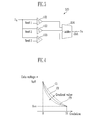
  • FIG. 3 is a view illustrating the A/D converter 120 employed in the organic light emitting display according to the first embodiment of the present invention.
  • the A/D converter 120 includes a first comparator 121, a second comparator 122, a third comparator 123, and an adder 124.
  • the first comparator 121 outputs a result of comparing an analog sensed signal S A with a first reference voltage Vref1. In the case where the analog sensed signal S A is higher than the first reference voltage Vref1, the first comparator 121 outputs '1'. By contrast, in the case where the analog sensed signal S A is lower than the first reference voltage Vref1, the first comparator 121 outputs '0'.
  • the second comparator 122 outputs a result of comparing the analog sensed signal S A with a second reference voltage Vref2.
  • the third comparator 123 outputs a result of comparing the analog sensed signal S A with a third reference voltage Vref3.
  • a range of the analog sensed signal S A corresponding to the same digital sensed signal S D can be changed by varying the first through third reference voltages Vref1, Vref2, Vref3.
  • the adder 124 outputs the digital sensed signal SD, which can be in 2 bits, by adding the result outputted from the comparators 121, 122, 123 thereto.
  • the A/D converter 120 of FIG. 3 will be described on the assumption that the first reference voltage Vref1 is of '1V'; the second reference voltage Vref2 is of '2V'; the third reference voltage Vref3 is of '3V'; and the brighter the neighboring light is, the higher the voltage of the analog sensed signal S A is.
  • the first through third comparators 121, 122 and 123 output '0', '0' and '0', respectively, so that the adder 124 outputs the digital signal S D of '00'.
  • the first through third comparators 121, 122 and 123 output '1', '0' and '0', respectively, so that the adder 124 outputs the digital signal S D of '01'.
  • the adder 124 outputs the digital signal S D of '10'.
  • the adder 124 outputs the digital signal S D of '11'.
  • the A/D converter 120 divides the neighboring brightness into four levels, and outputs '00' at the darkest case, '01' at a certain dark case, '10' at a certain bright case, and '11' at the brightest case.
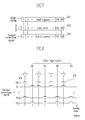
  • FIG. 4 is a graph showing a gamma correction value stored in a gamma correction value storage of the organic light emitting display according to the first embodiment of the present invention.
  • a horizontal axis indicates gradation
  • a vertical axis indicates a data voltage outputted from the driver 300 to the image displaying part 400.
  • the graph shows the data voltage corresponding to the gradation, which is called a gamma curve.
  • the gamma correction corrects nonlinear characteristics in the brightness of the image displaying part 400 with regard to RGB data inputted to the driver 300.
  • an off-voltage Voff indicates voltage corresponding to black (a gradation of '0'), and an on-voltage Von indicates voltage corresponding to white (a gradation of '15').
  • a gradient value indicates variance in a gradient. Referring to FIG. 4, the gradient of curve C2 is larger than that of curve C1 and smaller than that of curve C3.
  • the gamma correction values stored in the gamma correction value storage 220 can have all voltage levels (ranging from Von to Voff) corresponding to the respective gradations. In this case, the gamma correction is easily performed using the gamma correction values, but the storage 220 has to store all voltage levels corresponding to all gradations, thereby requiring a lot of memory.
  • the gamma correction values stored in the gamma correction value storage 220 can have some voltage levels corresponding to some gradations. In this case, the other voltage levels can be calculated by interpolating the stored voltage levels.
  • the gamma correction values stored in the gamma correction value storage 220 can include the off-voltage Voff, the on-voltage Von, and the gradient value.
  • each gamma curve shown in FIG. 4 can be calculated based on its off-voltage Voff, its on-voltage Von, and its gradient value.
  • the gamma correction values can include only the on-voltage Von and the gradient value.
  • FIG. 5 shows color coordinates of x and y to illustrate the storing of the different gamma correction values according to R, G, B in a gamma correction value storage of an organic light emitting display according to an embodiment of the present invention.
  • a coordinate value of x on an X-axis and a coordinate value of y on a Y-axis are represented as equation 1.
  • x X/(X+Y+Z)
  • y Y/(X+Y+Z)
  • X is the brightness of red
  • Y is the brightness of green
  • Z is the brightness of blue.
  • initial color coordinates of white can be deviated from the desired color coordinates of white and may be located in the red region "R", the green region “G” or the blue region “B” because of the difference in the processing conditions.
  • the gamma correction values are differently applied to red data, green data, and blue data, so that the color coordinates of the white can be corrected into the desired color coordinates.
  • FIG. 6 is a graph showing gamma correction values according to a sensing signal. As shown, C1' indicates a gamma curve corresponding to the sensed signal at the darkest case; C2' indicates a gamma curve corresponding to the sensed signal at the certain dark case; C3' indicates a gamma curve corresponding to the sensed signal at the certain bright case; and C4' indicates a gamma curve corresponding to the sensed signal at the brightest case.
  • the gamma correction value storage 220 stores the gamma correction values (or on-voltages) Von1, Von2, Von3 and Von4 corresponding to the respective gamma curves C1', C2', C3' and C4', and stores the gradient values of the respective gamma curves C1', C2', C3', and C4'.
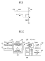
  • FIG. 7 is a view for illustrating a data driver (e.g., the data driver 320 of FIG. 1) employed in an organic light emitting display according to an embodiment of the present invention.
  • the data driver includes a shift register 321, a data latch 322, and a digital/analog (D/A) converter 323.
  • the shift register 321 controls the data latch 322 in correspondence with a horizontal clock signal HCLK and a horizontal synchronous signal HSYNC.
  • the data latch 322 receives the RGB data corresponding to a horizontal line of the shift register 321 in sequence, and transmits them to the D/A converter 323 in parallel. At this time, the data latch 322 is controlled on the basis of a control signal outputted from the shift register 321.
  • the D/A converter 323 converts the RGB data into the analog data signal, and transmits it to an image displaying part (e.g., the image displaying part 400 of FIG. 1). Further, the D/A converter 323 includes a plurality of D/A converting circuits (not shown). In each D/A converting circuit, current or voltage of the data signal corresponding to the respective gradations is determined according to one or more gamma correction signals.
  • FIG. 8 is a view for illustrating a D/A converter (e.g., the D/A converter 323 of FIG. 7) employed in a data driver according to an embodiment of the present invention, in which a digital data signal having 4 bits is illustrated.
  • the D/A converter includes a plurality of inverters 324, and a plurality of NMOS (N metal oxide semiconductor) transistors 325.
  • NMOS N metal oxide semiconductor
  • the digital data signals D 0 , D 1 , D 2 and D 3 which can be in 4 bits, and the signals (or inverted signals) from the digital data signals D 0 , D 1 , D 2 and D 3 passing through the inverters 324 are connected to the gate of each NMOS transistor 325, thereby turning on/off each NMOS transistor 325.
  • the respective gamma correction signals V 0 through V 15 are connected to four NMOS transistors 325 connected in series.
  • an analog data signal is outputted.
  • the digital data signal is '0001' as a binary number, that is, when D 0 is '1', D 1 is '0', D 2 is '0' and D 3 is '0', four NMOS transistors 325 connected to the gamma correction signal corresponding to "V 1 " are all turned on, thereby outputting the analog data signal corresponding to "V 1 ".
  • at least one of four NMOS transistors 325 connected to the other respective gamma correction signals is turned off, so that the other gamma correction signals are not outputted as the analog data signal.
  • the gamma correction signals V 0 through V 15 are inputted corresponding to all gradations of each digital data signal D 0 , D 1 , D 2 and D 3 .
  • the gamma correction signals corresponding to some gradations of the digital data signal may be inputted, and the other gradations can be calculated by interpolating the inputted gamma correction signals.
  • FIG. 9 is a circuit diagram of a pixel included in an image displaying part employed in the organic light emitting display according to the first embodiment of the present invention.
  • the pixel of the organic light emitting display includes an organic light emitting device OLED, a driving transistor MD, a capacitor C, and a switching transistor MS.
  • the driving transistor MD and the switching transistor MS can be realized by a thin film transistor.
  • Each of the driving and switching transistors MD and MS has a gate, a source and a drain.
  • the capacitor C includes a first terminal and a second terminal.
  • the switching transistor MS includes the gate connected to the scan line SCAN, the source connected to the gate of the driving transistor MD, and the drain connected to the data line DATA.
  • the switching transistor MS controls the capacitor C to store voltage corresponding to the data voltage applied to the data line DATA in response to the scan signal applied to the scan line SCAN.
  • the capacitor C includes the first terminal to which power voltage VDD is applied, and the second terminal connected to the gate of the driving transistor MD.
  • the capacitor C stores the voltage corresponding to the data voltage applied to the data line DATA while the switching transistor MS is turned on, and keeps the voltage while the switching transistor MS is turned off.
  • the driving transistor MD includes the gate connected to the second terminal of the capacitor C, the source to which the power voltage VDD is applied, and the drain connected to an anode electrode of the organic light emitting device OLED.
  • the driving transistor MD supplies a current corresponding to the voltage applied between the first and second terminals of the capacitor C to the organic light emitting display.
  • FIG. 10 is a block diagram of an organic light emitting display according to a second embodiment of the present invention.
  • an organic light emitting display according to the second embodiment of the present invention includes an optical sensing part 100, a gamma controller 200, a driver 600, and an image displaying part 400.
  • the optical sensing part 100, the gamma controller 200, and the image displaying part 400 have the same configuration as those of the first embodiment.
  • the driver 600 transmits a data signal to the image displaying part 400.
  • the data signal is corrected by using gamma correction according to a selection signal and a gamma correction value.
  • the driver 600 includes a gamma correction part 610, a data driver 620, and a scan driver 630.
  • the gamma correction part 610 also receives RGB data, and outputs the gamma-corrected RGB data to the data driver 620.
  • the data driver 620 outputs the data signal corresponding to the gamma-corrected RGB data to the image displaying part 400.
  • the scan driver 630 transmits the selection signal to the image displaying part 400.
  • the gamma correction part 610 outputs the data voltages corresponding to the respective gradations of the RGB data as the gamma-corrected RGB data.
  • each gradation of the RGB data is '0', off-voltage Voff is outputted as the gamma-corrected RGB data.
  • the data driver 620 outputs the data signal corresponding to the gamma-corrected RGB data.
  • the gradations of the gamma-corrected RGB data linearly correspond to the level of the data signals. That is, the level of the data signal is increased in proportion to the gradation of the gamma-corrected RGB data.
  • an embodiment of the present invention provides an organic light emitting display and a control method thereof, which can use a gamma correction value corresponding to a neighboring brightness and can control the brightness of the display to vary depending on the neighboring brightness, thereby lengthening lifespan of a pixel of the display and reducing power consumption.
  • an embodiment of the present invention provides a fabricated organic light emitting display and a control method thereof, which can use a programmable memory for storing a gamma correction value to thereby program a gamma correction value suitable for the fabricated organic light emitting display and/or a user.
  • an embodiment of the present invention provides a fabricated organic light emitting display and a control method thereof, which can use different gamma correction values according to R, G and B to thereby correct a color coordinate value of a white light emitted by the fabricated organic light emitting display.

Landscapes

  • Engineering & Computer Science (AREA)
  • Physics & Mathematics (AREA)
  • Computer Hardware Design (AREA)
  • General Physics & Mathematics (AREA)
  • Theoretical Computer Science (AREA)
  • Electroluminescent Light Sources (AREA)
  • Control Of El Displays (AREA)
  • Control Of Indicators Other Than Cathode Ray Tubes (AREA)

Abstract

An organic light emitting display and a control method thereof, which can control brightness of an image displaying part depending on neighboring brightness. The organic light emitting display includes: an optical sensing part for outputting a sensed signal corresponding to a neighboring brightness; a gamma controller for outputting a gamma correction value corresponding to the sensed signal; a driver for outputting a selection signal and a gamma-corrected data signal according to the gamma correction value; and an image displaying part for displaying an image according to the data signal and the selection signal outputted from the driver. In this configuration, the display uses the gamma correction value corresponding to neighboring brightness and controls the brightness of the display to vary depending on the neighboring brightness, thereby lengthening lifespan of a pixel of the display and reducing power consumption. <IMAGE>

Description

CROSS-REFERENCE TO RELATED APPLICATION
This application claims priority to and the benefit of Korean Patent Application No. 10-2004-0044683, filed on June 16, 2004, in the Korean Intellectual Property Office, the entire content of which is incorporated herein by reference.
BACKGROUND 1. Field of the Invention
The present invention relates to an organic light emitting display and a control method thereof, and more particularly, to an organic light emitting display and a control method thereof which can control brightness of an image displaying part depending on a neighboring brightness.
2. Discussion of Related Art
An organic electroluminescent display (or an organic light emitting display) is a display device based on a phenomenon that an exciton emits light of a specific wavelength in an organic thin film. The exciton is formed by recombination of an electron and a hole respectively injected from a cathode and an anode. Unlike a liquid crystal display (LCD), the organic electroluminescent display includes a self-emitting device, so that a separate light source is not needed. In the organic electroluminescent display, the brightness of an organic light emitting device or diode (OLED) varies according to the amount of current flowing into the organic light emitting device.
The organic electroluminescent display is classified into a passive matrix type and an active matrix type according to driving methods. In the case of the passive matrix type, the anode and the cathode are perpendicularly disposed and form a line to be selectively driven. The passive matrix type organic electroluminescent display can be easily formed due to a relatively simple structure, but is inadequate for forming a large-sized screen because it consumes a relatively large amount of power, and yet it drives each organic light emitting device to emit light for a relatively short period. On the other hand, in the case of the active matrix type, an active device is used to control the quantity of current flowing in the organic light emitting device. As the active device, a thin film transistor (hereinafter, referred to as "TFT") is widely used. The active matrix type organic electroluminescent display has a relatively complicated structure, but it consumes a relatively small amount of power, and yet it drives each organic light emitting device to emit light for a relatively long period.
Also, the life span of the organic light emitting device depends on the amount of current flowing therein. Because of this, when the organic light emitting device wastefully emits light at a high brightness, the amount of the current flowing in the organic light emitting device is increased, thereby shortening the life span of the organic light emitting device. Further, when the organic light emitting device wastefully emits light at a high brightness, the amount of the current flowing in the organic light emitting device is increased, thereby increasing power consumption. Therefore, the organic light emitting device should be controlled to emit proper brightness.
SUMMARY OF THE INVENTION
An embodiment of the present invention provides an organic light emitting display and a control method thereof, which can use a gamma correction value corresponding to a neighboring brightness (or a brightness of a neighboring region) and can control the brightness of the display to vary depending on the neighboring brightness.
An embodiment of the present invention provides a fabricated organic light emitting display and a control method thereof, which can use a programmable memory for storing a gamma correction value to thereby program a gamma correction value suitable (or customized) for the fabricated organic light emitting display and/or a user.
An embodiment of the present invention provides a fabricated organic light emitting display and a control method thereof, which can use different gamma correction values according to red (R), green (G) and blue (B) to thereby correct a color coordinate value of a white light emitted by fabricated organic light emitting display.
One embodiment of the present invention provides an organic light emitting display including: an optical sensing part for outputting a sensed signal corresponding to a neighboring brightness of the organic light emitting display; a gamma controller for outputting a gamma correction value corresponding to the sensed signal; a driver for outputting a selection signal and a gamma-corrected data signal according to the gamma correction value; and an image displaying part for displaying an image according to the gamma-corrected data signal and the selection signal outputted from the driver.
In one embodiment of the invention, the gamma controller includes a sensed signal processor for outputting a storage control signal corresponding to the sensed signal; and a gamma correction value storage for outputting a gamma correction value according to the storage control signal. Further, in one embodiment of the invention, the gamma correction value storage includes a programmable memory. Also, in one embodiment of the invention, the gamma correction value include a plurality of different gamma correction value, and the gamma correction value storage stores the plurality of different gamma correction values according to red (R), green (G) and blue (B).
One embodiment of the present invention provides a method of controlling an organic light emitting display, the method including: sensing a neighboring brightness of the organic light emitting display; reading a gamma correction value corresponding to the sensed neighboring brightness from a gamma correction value storage for storing a plurality of gamma correction values; generating a selection signal and a gamma-corrected data signal based on the read gamma correction value; and displaying an image on an image displaying part of the organic light emitting display in accordance with the selection signal and the gamma-corrected data signal.
In one embodiment of the invention, the gamma correction value storage includes a programmable memory. Further, in one embodiment of the invention the gamma correction value includes a plurality of different gamma correction values, and the gamma correction value storage stores the plurality of different gamma correction values according to R, G and B.
BRIEF DESCRIPTION OF THE DRAWINGS
The accompanying drawings, together with the specification, illustrate exemplary embodiments of the present invention, and, together with the description, serve to explain the principles of the invention.
FIG. 1 is a block diagram of an organic light emitting display according to a first embodiment of the present invention;
FIG. 2 is a perspective view of a terminal such as a mobile phone provided with an optical sensor according to the first embodiment of the present invention;
FIG. 3 is a view illustrating an A/D converter employed in the organic light emitting display according to the first embodiment of the present invention;
FIG. 4 is a graph showing a gamma correction value stored in a gamma correction value storage of the organic light emitting display according to the first embodiment of the present invention;
FIG. 5 shows color coordinates of x and y in order to illustrate the storing of the different gamma correction values according to R, G, B in a gamma correction value storage of an organic light emitting display according to an embodiment of the present invention;
FIG. 6 is a graph showing gamma correction values according to a sensing signal;
FIG. 7 is a view for illustrating a data driver employed in an organic light emitting display according to an embodiment of the present invention;
FIG. 8 is a view for illustrating a D/A converter employed in a data driver according to an embodiment of the present invention;
FIG. 9 is a circuit diagram of a pixel included in an image displaying part employed in the organic light emitting display according to the first embodiment of the present invention; and
FIG. 10 is a block diagram of an organic light emitting display according to a second embodiment of the present invention.
DETAILED DESCRIPTION
In the following detailed description, only certain exemplary embodiments of the present invention are shown and described, simply by way of illustration. As those skilled in the art would realize, the described embodiments may be modified in various different ways, all without departing from the spirit or scope of the present invention.
FIG. 1 is a block diagram of an organic light emitting display according to a first embodiment of the present invention. As shown, the organic light emitting display according to the first embodiment of the present invention includes an optical sensing part 100, a gamma controller 200, a driver 300, and an image displaying part 400.
The optical sensing part 100 senses a neighboring brightness, and outputs a sensed signal corresponding to the neighboring brightness to the gamma controller 200. The optical sensing part 100 includes an optical sensor 110 and an analog/digital (A/D) converter 120. The optical sensor 110 senses the neighboring brightness, and outputs an analog sensed signal. Here, the analog sensed signal may be a voltage signal or a current signal. For example, the optical sensor 110 includes a photoresistor using a phenomenon that resistance of a resistor varies according to incident light; a photodiode using a phenomenon that current flows due to an electron-hole pair generated when light is emitted to a PN-junction of a semiconductor; a phototransistor amplifying photocurrent between a base and a collector of the photodiode; a complementary metal oxide semiconductor (CMOS); a charge-coupled device (CCD); etc. The A/D converter 120 converts the analog sensed signal output from the optical sensor 110 into a digital sensed signal.
The gamma controller 200 outputs a gamma correction value to the driver 300 in correspondence with the sensed signal output from the optical sensing part 100. The gamma controller 200 includes a sensed signal processor 210, and a gamma correction storage 220. The sensed signal processor 210 outputs a storage control signal for controlling the gamma correction value storage 220 to output the gamma correction value corresponding to the sensed signal. The gamma correction value storage 200 stores a plurality of gamma correction values corresponding to the sensed signals, and outputs the gamma correction value corresponding to the storage control signal to a gamma correction part 310. The gamma correction storage can store the different gamma correction values according to red (R), green (G) and blue (B). Here, the gamma correction value storage 220 may be a programmable memory. By way of example, the programmable memory includes a programmable read only memory (PROM) that allows programming only once; an erasable programmable read only memory (EPROM) that allows reprogramming; an electrically erasable programmable read only memory (EEPROM) that allows electrical reprogramming; a flash memory, etc. Here, the sensed signal processor 210 can be used to program the gamma correction value storage 220. Alternatively, a separate storage control unit may be used to program the gamma correction value storage 220. The gamma correction value storage 220 is programmable, so that it is possible to program and/or customize a suitable gamma correction value for the fabricated organic light emitting display and/or a user. In more detail, characteristics of fabricated image displaying parts (e.g., part 400) may be affected by variances in processing conditions, so that the characteristics of the fabricated image displaying parts may be varied according to the fabrication of the fabricated image displaying parts. Therefore, in a case of a non-programmable memory, because an invariable gamma correction value is applied to the fabricated image displaying parts, it may be inadequate to reflect the individual brightness characteristics of the fabricated image displaying part 400, so that the gamma correction may not be properly performed. Because of this, in one embodiment of the present invention, a programmable memory is used to store the gamma correction value suitable for the fabricated image displaying part 400, and therefore the organic light emitting display can have the desired brightness even though there may be differences in the processing conditions.
The driver 300 is employed to transmit the data signal to the image displaying part 400. The data signal is corrected using the gamma correction according to the selection signals and the gamma correction values. The driver 300 includes the gamma correction part 310, the data driver 320, and the scan driver 330. The gamma correction part 310 generates a gamma correction signal corresponding to the gamma correction value outputted from the gamma correction value storage 220, and outputs the gamma correction signal to the data driver 320. Then, the data driver 320 transmits the data signal to the image displaying part 400. The data signal is corrected using the gamma correction based on the gamma correction signal. Further, the scan driver 330 transmits the selection signal to the image displaying part 400.
The image displaying part 400 includes a plurality of pixels (not shown), and provides the data signal from the data driver 320 to the pixel selected by the selection signal of the scan driver 330, thereby allowing the pixel to emit light corresponding to the data signal. Because of this, the organic light emitting display of FIG. 1 operates to thereby display an image corresponding to the data signal inputted to the driver 300. Further, based on the gamma correction value corresponding to the sensed signal outputted from the optical sensing part 100, the brightness of the image displaying part 400 can be adjusted in correspondence with the neighboring brightness. Also, the programmable memory can be used as the gamma correction value storage 220, so that the gamma correction value suitable (or customized) for the fabricated image displaying part 400 can be stored in the storage 220. Also, based on the different gamma correction values according to R, G and B, the organic light emitting display of FIG. 1 can have a desired value for color coordinates of white.
FIG. 2 is a perspective view of a terminal such as a mobile phone provided with an optical sensor according to the first embodiment of the present invention. As shown, the terminal includes the image displaying part 400, a first body 510, a second body 520, and the optical sensor 110.
The first body 510 and the second body 520 form a body of the terminal provided with the A/D converter 120, the gamma controller 200, and the driver 300. Further, the body of the terminal 510 and 520 includes an antenna 521, a radio frequency (RF) transceiver (not shown), and a baseband processor (not shown), thereby performing wireless communication.
The optical sensor 110 can be placed on any surface of the body of the terminal 510 and 520. In one embodiment, the optical sensor 110 is placed on the same surface as the image displaying part 400 is placed. That is, the brightness of the image displaying part 400 should be adjusted in correspondence to the incident brightness emitted toward (or the brightness falling upon) the image displaying part 400. However, since it is not easy to place the optical sensor 110 directly on the image displaying part 400, the optical sensor 110 in one embodiment is placed on the same surface of the terminal as the image displaying part 400 is placed, thereby sensing the brightness (or the neighboring brightness) of the nearest (or neighboring) light to the image displaying part 400. Further, the optical sensor 110 can be placed in upper, lower, left and/or right neighboring portions of the image displaying part 400 on the same surface of the terminal where the image displaying part 400 is placed.
FIG. 3 is a view illustrating the A/D converter 120 employed in the organic light emitting display according to the first embodiment of the present invention. As shown, the A/D converter 120 includes a first comparator 121, a second comparator 122, a third comparator 123, and an adder 124. The first comparator 121 outputs a result of comparing an analog sensed signal SA with a first reference voltage Vref1. In the case where the analog sensed signal SA is higher than the first reference voltage Vref1, the first comparator 121 outputs '1'. By contrast, in the case where the analog sensed signal SA is lower than the first reference voltage Vref1, the first comparator 121 outputs '0'. Likewise, the second comparator 122 outputs a result of comparing the analog sensed signal SA with a second reference voltage Vref2. The third comparator 123 outputs a result of comparing the analog sensed signal SA with a third reference voltage Vref3. Here, a range of the analog sensed signal SA corresponding to the same digital sensed signal SD can be changed by varying the first through third reference voltages Vref1, Vref2, Vref3. Further, the adder 124 outputs the digital sensed signal SD, which can be in 2 bits, by adding the result outputted from the comparators 121, 122, 123 thereto.
Hereinafter, the A/D converter 120 of FIG. 3 will be described on the assumption that the first reference voltage Vref1 is of '1V'; the second reference voltage Vref2 is of '2V'; the third reference voltage Vref3 is of '3V'; and the brighter the neighboring light is, the higher the voltage of the analog sensed signal SA is. When the analog sensed signal SA is lower than '1V', the first through third comparators 121, 122 and 123 output '0', '0' and '0', respectively, so that the adder 124 outputs the digital signal SD of '00'. When the analog sensed signal SA ranges between '1V' and '2V', the first through third comparators 121, 122 and 123 output '1', '0' and '0', respectively, so that the adder 124 outputs the digital signal SD of '01'. Likewise, when the analog sensed signal SA ranges between '2V' and '3V', the adder 124 outputs the digital signal SD of '10'. Further, when the analog sensed signal SA is higher than '3V', the adder 124 outputs the digital signal SD of '11'. Thus, the A/D converter 120 divides the neighboring brightness into four levels, and outputs '00' at the darkest case, '01' at a certain dark case, '10' at a certain bright case, and '11' at the brightest case.
FIG. 4 is a graph showing a gamma correction value stored in a gamma correction value storage of the organic light emitting display according to the first embodiment of the present invention. As shown, a horizontal axis indicates gradation, and a vertical axis indicates a data voltage outputted from the driver 300 to the image displaying part 400. Here, the graph shows the data voltage corresponding to the gradation, which is called a gamma curve. The gamma correction corrects nonlinear characteristics in the brightness of the image displaying part 400 with regard to RGB data inputted to the driver 300. Further, an off-voltage Voff indicates voltage corresponding to black (a gradation of '0'), and an on-voltage Von indicates voltage corresponding to white (a gradation of '15'). Also, a gradient value indicates variance in a gradient. Referring to FIG. 4, the gradient of curve C2 is larger than that of curve C1 and smaller than that of curve C3.
The gamma correction values stored in the gamma correction value storage 220 can have all voltage levels (ranging from Von to Voff) corresponding to the respective gradations. In this case, the gamma correction is easily performed using the gamma correction values, but the storage 220 has to store all voltage levels corresponding to all gradations, thereby requiring a lot of memory. Alternatively, the gamma correction values stored in the gamma correction value storage 220 can have some voltage levels corresponding to some gradations. In this case, the other voltage levels can be calculated by interpolating the stored voltage levels. Further, the gamma correction values stored in the gamma correction value storage 220 can include the off-voltage Voff, the on-voltage Von, and the gradient value. Thus, each gamma curve shown in FIG. 4 can be calculated based on its off-voltage Voff, its on-voltage Von, and its gradient value. In the case where the off-voltage Voff is invariable, the gamma correction values can include only the on-voltage Von and the gradient value.
FIG. 5 shows color coordinates of x and y to illustrate the storing of the different gamma correction values according to R, G, B in a gamma correction value storage of an organic light emitting display according to an embodiment of the present invention.
In FIG. 5, a coordinate value of x on an X-axis and a coordinate value of y on a Y-axis are represented as equation 1. <equation 1> x = X/(X+Y+Z), y = Y/(X+Y+Z) where X is the brightness of red, Y is the brightness of green, and Z is the brightness of blue.
In FIG. 5, "W" indicates the color coordinates of white, e.g., x = 0.31, y = 0.316; "R" indicates a region representing color near red; "G" indicates a region representing color near green; and "B" indicates a region representing color near blue.
In a fabricated image displaying part, initial color coordinates of white can be deviated from the desired color coordinates of white and may be located in the red region "R", the green region "G" or the blue region "B" because of the difference in the processing conditions. In this case, the gamma correction values are differently applied to red data, green data, and blue data, so that the color coordinates of the white can be corrected into the desired color coordinates.
FIG. 6 is a graph showing gamma correction values according to a sensing signal. As shown, C1' indicates a gamma curve corresponding to the sensed signal at the darkest case; C2' indicates a gamma curve corresponding to the sensed signal at the certain dark case; C3' indicates a gamma curve corresponding to the sensed signal at the certain bright case; and C4' indicates a gamma curve corresponding to the sensed signal at the brightest case. In one embodiment, the gamma correction value storage 220 stores the gamma correction values (or on-voltages) Von1, Von2, Von3 and Von4 corresponding to the respective gamma curves C1', C2', C3' and C4', and stores the gradient values of the respective gamma curves C1', C2', C3', and C4'.
FIG. 7 is a view for illustrating a data driver (e.g., the data driver 320 of FIG. 1) employed in an organic light emitting display according to an embodiment of the present invention. As shown, the data driver includes a shift register 321, a data latch 322, and a digital/analog (D/A) converter 323. The shift register 321 controls the data latch 322 in correspondence with a horizontal clock signal HCLK and a horizontal synchronous signal HSYNC. The data latch 322 receives the RGB data corresponding to a horizontal line of the shift register 321 in sequence, and transmits them to the D/A converter 323 in parallel. At this time, the data latch 322 is controlled on the basis of a control signal outputted from the shift register 321. The D/A converter 323 converts the RGB data into the analog data signal, and transmits it to an image displaying part (e.g., the image displaying part 400 of FIG. 1). Further, the D/A converter 323 includes a plurality of D/A converting circuits (not shown). In each D/A converting circuit, current or voltage of the data signal corresponding to the respective gradations is determined according to one or more gamma correction signals.
FIG. 8 is a view for illustrating a D/A converter (e.g., the D/A converter 323 of FIG. 7) employed in a data driver according to an embodiment of the present invention, in which a digital data signal having 4 bits is illustrated. As shown, the D/A converter includes a plurality of inverters 324, and a plurality of NMOS (N metal oxide semiconductor) transistors 325. The digital data signals D0, D1, D2 and D3, which can be in 4 bits, and the signals (or inverted signals) from the digital data signals D0, D1, D2 and D3 passing through the inverters 324 are connected to the gate of each NMOS transistor 325, thereby turning on/off each NMOS transistor 325. The respective gamma correction signals V0 through V15 are connected to four NMOS transistors 325 connected in series. Therefore, when four NMOS transistors 325 are all turned on by the digital data signals D0, D1, D2 and D3 and the signals from the digital data signals D0, D1, D2 and D3 passing through the inverters 324, an analog data signal is outputted. For example, when the digital data signal is '0001' as a binary number, that is, when D0 is '1', D1 is '0', D2 is '0' and D3 is '0', four NMOS transistors 325 connected to the gamma correction signal corresponding to "V1" are all turned on, thereby outputting the analog data signal corresponding to "V1". At this time, at least one of four NMOS transistors 325 connected to the other respective gamma correction signals is turned off, so that the other gamma correction signals are not outputted as the analog data signal.
In the embodiment of FIG. 8, the gamma correction signals V0 through V15 are inputted corresponding to all gradations of each digital data signal D0, D1, D2 and D3. Alternatively, the gamma correction signals corresponding to some gradations of the digital data signal may be inputted, and the other gradations can be calculated by interpolating the inputted gamma correction signals.
FIG. 9 is a circuit diagram of a pixel included in an image displaying part employed in the organic light emitting display according to the first embodiment of the present invention. As shown, the pixel of the organic light emitting display includes an organic light emitting device OLED, a driving transistor MD, a capacitor C, and a switching transistor MS. The driving transistor MD and the switching transistor MS can be realized by a thin film transistor. Each of the driving and switching transistors MD and MS has a gate, a source and a drain. The capacitor C includes a first terminal and a second terminal.
The switching transistor MS includes the gate connected to the scan line SCAN, the source connected to the gate of the driving transistor MD, and the drain connected to the data line DATA. Here, the switching transistor MS controls the capacitor C to store voltage corresponding to the data voltage applied to the data line DATA in response to the scan signal applied to the scan line SCAN.
The capacitor C includes the first terminal to which power voltage VDD is applied, and the second terminal connected to the gate of the driving transistor MD. Here, the capacitor C stores the voltage corresponding to the data voltage applied to the data line DATA while the switching transistor MS is turned on, and keeps the voltage while the switching transistor MS is turned off.
The driving transistor MD includes the gate connected to the second terminal of the capacitor C, the source to which the power voltage VDD is applied, and the drain connected to an anode electrode of the organic light emitting device OLED. Here, the driving transistor MD supplies a current corresponding to the voltage applied between the first and second terminals of the capacitor C to the organic light emitting display.
FIG. 10 is a block diagram of an organic light emitting display according to a second embodiment of the present invention. As shown, an organic light emitting display according to the second embodiment of the present invention includes an optical sensing part 100, a gamma controller 200, a driver 600, and an image displaying part 400. According to the second embodiment of the present invention, the optical sensing part 100, the gamma controller 200, and the image displaying part 400 have the same configuration as those of the first embodiment.
The driver 600 transmits a data signal to the image displaying part 400. The data signal is corrected by using gamma correction according to a selection signal and a gamma correction value. The driver 600 includes a gamma correction part 610, a data driver 620, and a scan driver 630. In the embodiment of FIG. 10, the gamma correction part 610 also receives RGB data, and outputs the gamma-corrected RGB data to the data driver 620. The data driver 620 outputs the data signal corresponding to the gamma-corrected RGB data to the image displaying part 400. The scan driver 630 transmits the selection signal to the image displaying part 400.
In more detail, the gamma correction part 610 and the data driver 620 will be described hereinbelow with respect to FIGs. 4 and 10. The gamma correction part 610 outputs the data voltages corresponding to the respective gradations of the RGB data as the gamma-corrected RGB data. In the case where each gradation of the RGB data is '0', off-voltage Voff is outputted as the gamma-corrected RGB data. The data driver 620 outputs the data signal corresponding to the gamma-corrected RGB data. The gradations of the gamma-corrected RGB data linearly correspond to the level of the data signals. That is, the level of the data signal is increased in proportion to the gradation of the gamma-corrected RGB data.
In general, an embodiment of the present invention provides an organic light emitting display and a control method thereof, which can use a gamma correction value corresponding to a neighboring brightness and can control the brightness of the display to vary depending on the neighboring brightness, thereby lengthening lifespan of a pixel of the display and reducing power consumption.
Further, an embodiment of the present invention provides a fabricated organic light emitting display and a control method thereof, which can use a programmable memory for storing a gamma correction value to thereby program a gamma correction value suitable for the fabricated organic light emitting display and/or a user.
Also, an embodiment of the present invention provides a fabricated organic light emitting display and a control method thereof, which can use different gamma correction values according to R, G and B to thereby correct a color coordinate value of a white light emitted by the fabricated organic light emitting display.
While the invention has been described in connection with certain exemplary embodiments, it is to be understood by those skilled in the art that the invention is not limited to the disclosed embodiments, but, on the contrary, is intended to cover various modifications included within the spirit and scope of the appended claims and equivalents thereof.

Claims (20)

  1. An organic light emitting display comprising:
    an optical sensing part for outputting a sensed signal corresponding to a neighboring brightness of the organic light emitting display;
    a gamma controller for outputting a gamma correction value corresponding to the sensed signal;
    a driver for outputting a selection signal and a gamma-corrected data signal according to the gamma correction value; and
    an image displaying part for displaying an image according to the gamma-corrected data signal and the selection signal outputted from the driver.
  2. The organic light emitting display according to claim 1, wherein the optical sensing part comprises:
    an optical sensor for outputting an analog sensed signal corresponding to the neighboring brightness; and
    an analog/digital (A/D) converter for converting the analog sensed signal into the sensed signal, wherein the sensed signal is a digital sensed signal.
  3. The organic light emitting display according to claim 2, wherein the optical sensor includes a photoresistor, a photodiode, a phototransistor, a complementary metal oxide semiconductor (CMOS), and/or a charge-coupled device (CCD).
  4. The organic light emitting display according to claim 2, wherein the A/D converter comprises:
    a plurality of comparators, each of the plurality of comparators being for outputting a result of comparing the analog sensed signal with a predetermined reference signal; and
    an adder for adding the results outputted by the comparators.
  5. The organic light emitting display according to claim 1, wherein the gamma controller comprises:
    a sensed signal processor for outputting a storage control signal corresponding to the sensed signal; and
    a gamma correction value storage for outputting a gamma correction value according to the storage control signal.
  6. The organic light emitting display according to claim 5, wherein the gamma correction value storage includes a programmable memory.
  7. The organic light emitting display according to claim 6, wherein the programmable memory includes a programmable read only memory (PROM), an erasable programmable read only memory (EPROM), an electrically erasable programmable read only memory (EEPROM), and/or a flash memory.
  8. The organic light emitting display according to claim 5, wherein the gamma correction value comprises a plurality of different gamma correction values and wherein the gamma correction value storage stores the plurality of different gamma correction values according to red (R), green (G) and blue (B).
  9. The organic light emitting display according to claim 5, wherein the gamma correction value includes:
    an on-voltage value corresponding to a gradation of white; and
    a gradient value for indicating a variance in a gradient of a gamma curve.
  10. The organic light emitting display according to claim 9, wherein the gamma correction value further includes an off-voltage value corresponding to a gradation of black.
  11. The organic light emitting display according to claim 1, wherein the driver comprises:
    a gamma correction part for outputting a gamma correction signal corresponding to the gamma correction value;
    a data driver for outputting the gamma-corrected data signal corresponding to the gamma correction signal; and
    a scan driver for outputting the selection signal.
  12. The organic light emitting display according to claim 11, wherein the data driver comprises:
    a shift register for outputting a latch control signal corresponding to a clock signal and a synchronization signal;
    a data latch for sequentially receiving and for parallel outputting RGB data according to the latch control signal; and
    a digital/analog (D/A) converter for converting the RGB data outputted by the data latch into an analog signal and for outputting the analog signal as the data signal, wherein the data signal corresponding to each gradation is determined by the gamma correction signal.
  13. The organic light emitting display according to claim 1, wherein the driver comprises:
    a gamma correction part for receiving input RGB data and for applying gamma correction to the input RGB data corresponding to the gamma correction value;
    a data driver for outputting the data signal corresponding to the gamma-corrected RGB data; and
    a scan driver for outputting the selection signal.
  14. A method of controlling an organic light emitting display, the method comprising:
    sensing a neighboring brightness of the organic light emitting display;
    reading a gamma correction value corresponding to the sensed neighboring brightness from a gamma correction value storage for storing a plurality of gamma correction values;
    generating a selection signal and a gamma-corrected data signal based on the read gamma correction value; and
    displaying an image on an image displaying part of the organic light emitting display in accordance with the selection signal and the gamma-corrected data signal.
  15. The method according to claim 14, wherein the gamma correction value storage includes a programmable memory.
  16. The method according to claim 15, wherein the programmable memory includes a programmable read only memory (PROM), an erasable programmable read only memory (EPROM), an electrically erasable programmable read only memory (EEPROM), and/or a flash memory.
  17. The method according to claim 14, wherein the gamma correction value comprises a plurality of different gamma correction values and wherein the gamma correction value storage stores the plurality of different gamma correction values according to red (R), green (G) and blue (B).
  18. The method according to claim 14, wherein the gamma correction value includes:
    an on-voltage value for corresponding to a gradation of white; and
    a gradient value for indicating a variance in a gradient of a gamma curve.
  19. The method according to claim 18, wherein the gamma correction value further includes an off-voltage value corresponding to a gradation of black.
  20. An organic light emitting display comprising:
    means for sensing a neighboring brightness of the organic light emitting display;
    means for reading a gamma correction value corresponding to the sensed neighboring brightness from a plurality of stored gamma correction values;
    means for generating a selection signal and a gamma-corrected data signal based on the read gamma correction value; and
    means for displaying an image on an image displaying part of the organic light emitting display corresponding with the selection signal and the gamma-corrected data signal.
EP05104919A 2004-06-16 2005-06-07 Organic light emitting display and control method thereof Withdrawn EP1607932A1 (en)

Applications Claiming Priority (2)

Application Number Priority Date Filing Date Title
KR1020040044683A KR100646996B1 (en) 2004-06-16 2004-06-16 OLED display and control method thereof
KR2004044683 2004-06-16

Publications (1)

Publication Number Publication Date
EP1607932A1 true EP1607932A1 (en) 2005-12-21

Family

ID=34940089

Family Applications (1)

Application Number Title Priority Date Filing Date
EP05104919A Withdrawn EP1607932A1 (en) 2004-06-16 2005-06-07 Organic light emitting display and control method thereof

Country Status (5)

Country Link
US (1) US20060001624A1 (en)
EP (1) EP1607932A1 (en)
JP (1) JP2006003874A (en)
KR (1) KR100646996B1 (en)
CN (1) CN100538791C (en)

Cited By (2)

* Cited by examiner, † Cited by third party
Publication number Priority date Publication date Assignee Title
EP1962268A1 (en) * 2007-02-23 2008-08-27 Samsung SDI Co., Ltd. Organic elecroluminescence display (OLED) and driving methods thereof
CN101256097B (en) * 2006-12-27 2010-11-10 三星移动显示器株式会社 Ambient light detection circuit and flat panel display including the ambient light detection circuit

Families Citing this family (44)

* Cited by examiner, † Cited by third party
Publication number Priority date Publication date Assignee Title
KR100662980B1 (en) * 2004-07-23 2006-12-28 삼성에스디아이 주식회사 Light emitting display
KR100624366B1 (en) * 2005-06-29 2006-09-15 엘지.필립스 엘시디 주식회사 Display device and dynamic gamma application method
CN100468495C (en) * 2006-01-27 2009-03-11 华硕电脑股份有限公司 Display device capable of compensating ambient brightness
WO2007099944A1 (en) * 2006-03-01 2007-09-07 Nec Corporation Mobile telephone terminal, screen display control method used for the same, and program thereof
KR100745982B1 (en) 2006-06-19 2007-08-06 삼성전자주식회사 Image processing apparatus and method for reducing power of self-luminous display
KR100841366B1 (en) * 2006-08-01 2008-06-26 삼성에스디아이 주식회사 Organic light emitting display device and driving method thereof
KR100809700B1 (en) * 2006-08-30 2008-03-07 삼성전자주식회사 Ambient light processing system that detects ambient light and controls the display device and method of using the system
KR100830297B1 (en) 2006-09-26 2008-05-19 삼성에스디아이 주식회사 Organic light emitting display device and driving method thereof
KR100825411B1 (en) * 2006-12-27 2008-04-29 한양대학교 산학협력단 Ambient light sensing circuit and flat panel display device having the same
EP1939847B1 (en) 2006-12-27 2016-08-10 IUCF-HYU (Industry-University Cooperation Foundation Hanyang University) Ambient light sensor circuit and flat panel display device having the same
JP4959449B2 (en) 2006-12-27 2012-06-20 三星モバイルディスプレイ株式會社 Ambient light sensing circuit and flat panel display having the same
JP5259132B2 (en) 2006-12-27 2013-08-07 三星ディスプレイ株式會社 Ambient light sensing circuit and flat panel display having the same
KR100836433B1 (en) * 2007-02-05 2008-06-09 삼성에스디아이 주식회사 Organic EL display device and driving method thereof
KR100836425B1 (en) * 2007-02-05 2008-06-09 삼성에스디아이 주식회사 Organic EL display device and driving method thereof
KR100836423B1 (en) * 2007-02-05 2008-06-09 삼성에스디아이 주식회사 Organic EL display device and driving method thereof
KR100836432B1 (en) * 2007-02-05 2008-06-09 삼성에스디아이 주식회사 Organic EL display device and driving method thereof
KR100840102B1 (en) * 2007-02-23 2008-06-19 삼성에스디아이 주식회사 Organic electroluminescent display
KR100844775B1 (en) * 2007-02-23 2008-07-07 삼성에스디아이 주식회사 Organic electroluminescent display
US20080252572A1 (en) * 2007-04-10 2008-10-16 Kinyeng Kang Organic electroluminescent display and image correction method thereof
KR101453970B1 (en) * 2007-09-04 2014-10-21 삼성디스플레이 주식회사 Organic light emitting display and method for driving thereof
KR20090037210A (en) * 2007-10-11 2009-04-15 삼성전자주식회사 Display Device and Gamma Data Adjustment Method
CN101882412B (en) * 2009-05-06 2013-04-10 奇菱科技股份有限公司 Detection and correction system for flat panel displays and flat panel displays
KR101329966B1 (en) 2009-09-22 2013-11-20 엘지디스플레이 주식회사 Appratus and method for controlling brightness of organic light emitting diode display
JP5556215B2 (en) * 2010-02-10 2014-07-23 日本電気株式会社 Image quality adjustment method for display unit using camera for portable device, apparatus and program thereof
KR101147419B1 (en) 2010-05-04 2012-05-22 삼성모바일디스플레이주식회사 Display device and establishing method of gamma for the same
KR101439333B1 (en) 2010-09-14 2014-09-11 삼성디스플레이 주식회사 Luminance Correction System for Organic Light Emitting Display Device
US9666119B2 (en) * 2012-08-30 2017-05-30 Apple Inc. Systems and methods for controlling current in display devices
KR101969830B1 (en) 2012-08-31 2019-08-14 삼성디스플레이 주식회사 Method of generating gamma correction curves, gamma correction unit, and organic light emitting display device having the same
CN103824549B (en) * 2013-12-25 2017-04-19 深圳市华星光电技术有限公司 Driving system architecture of liquid crystal display panel, and liquid crystal display (LCD) applying same
US9287890B2 (en) * 2014-05-12 2016-03-15 Olympus Corporation Analog-to-digital converter and solid-state imaging apparatus
KR102323358B1 (en) * 2014-11-06 2021-11-09 삼성디스플레이 주식회사 Organic Light Emitting Display Device and Display Method Thereof
CN107832029B (en) * 2014-11-28 2020-08-25 Oppo广东移动通信有限公司 Display processing method and device, terminal and computer readable storage medium
CN104581056B (en) * 2014-12-23 2019-01-15 深圳市锐明技术股份有限公司 A kind of method and device based on photosensitive sensor assisted image adjustment
CN105070252B (en) * 2015-08-13 2018-05-08 小米科技有限责任公司 Reduce the method and device of display brightness
KR102562645B1 (en) * 2016-05-20 2023-08-02 삼성전자주식회사 Operating Method for display corresponding to luminance, driving circuit, and electronic device supporting the same
US10431139B2 (en) * 2017-07-25 2019-10-01 Lenovo (Singapore) Pte. Ltd. Screen color calibration
CN108630145A (en) * 2018-06-26 2018-10-09 江苏集萃有机光电技术研究所有限公司 A kind of silicon substrate drive substrate and OLED display
TWI688930B (en) * 2019-02-11 2020-03-21 友達光電股份有限公司 Electronic device and driving method thereof
KR102671311B1 (en) * 2019-03-20 2024-06-04 삼성디스플레이 주식회사 Luminance control unit and display device including the same
CN111916031B (en) * 2019-05-10 2023-03-21 京东方科技集团股份有限公司 Display method and display device
KR102701957B1 (en) 2019-12-31 2024-09-02 엘지디스플레이 주식회사 Display apparatus
CN111540310A (en) * 2020-06-28 2020-08-14 厦门理工学院 A dimming method, device, device and readable storage medium for a Micro-LED display screen
KR102739393B1 (en) * 2020-10-08 2024-12-05 엘지디스플레이 주식회사 Display device, control circuit and driving method for the same
CN116994515B (en) * 2023-09-26 2023-12-12 昇显微电子(苏州)股份有限公司 Quick gamma correction method based on gradient descent

Citations (6)

* Cited by examiner, † Cited by third party
Publication number Priority date Publication date Assignee Title
US20030001815A1 (en) * 2001-06-28 2003-01-02 Ying Cui Method and apparatus for enabling power management of a flat panel display
US20030043137A1 (en) * 2001-09-03 2003-03-06 Nec Corporation Method of calibrating luminance of display, driving circuit of display employing same method and portable electronic device provided with same driving circuit
EP1335347A1 (en) * 2002-02-08 2003-08-13 Seiko Epson Corporation Reference voltage generation circuit and method, display driver circuit and liquid crystal display device
US20040012340A1 (en) * 2002-04-03 2004-01-22 Sanyo Electric Co., Ltd. Organic EL display device
US20040032382A1 (en) * 2000-09-29 2004-02-19 Cok Ronald S. Flat-panel display with luminance feedback
US20040036706A1 (en) * 2002-08-26 2004-02-26 Shinji Endou Display panel driver

Family Cites Families (11)

* Cited by examiner, † Cited by third party
Publication number Priority date Publication date Assignee Title
US6023532A (en) * 1994-03-25 2000-02-08 Seiko Epson Corporation Image reading apparatus, method and system
JP3236243B2 (en) * 1997-06-11 2001-12-10 キヤノン株式会社 Electroluminescence device and driving method thereof
US6373423B1 (en) * 1999-12-14 2002-04-16 National Instruments Corporation Flash analog-to-digital conversion system and method with reduced comparators
US6995753B2 (en) * 2000-06-06 2006-02-07 Semiconductor Energy Laboratory Co., Ltd. Display device and method of manufacturing the same
TW554625B (en) * 2000-12-08 2003-09-21 Silicon Graphics Inc Compact flat panel color calibration system
JP3902741B2 (en) * 2002-01-25 2007-04-11 株式会社半導体理工学研究センター Semiconductor integrated circuit device
JP3854161B2 (en) * 2002-01-31 2006-12-06 株式会社日立製作所 Display device
JP2004287118A (en) * 2003-03-24 2004-10-14 Hitachi Ltd Display device
US7262753B2 (en) * 2003-08-07 2007-08-28 Barco N.V. Method and system for measuring and controlling an OLED display element for improved lifetime and light output
US7528810B2 (en) * 2004-05-25 2009-05-05 Victor Company Of Japan, Limited Display with multiple emission layers
KR100748319B1 (en) * 2006-03-29 2007-08-09 삼성에스디아이 주식회사 OLED display device and driving method thereof

Patent Citations (6)

* Cited by examiner, † Cited by third party
Publication number Priority date Publication date Assignee Title
US20040032382A1 (en) * 2000-09-29 2004-02-19 Cok Ronald S. Flat-panel display with luminance feedback
US20030001815A1 (en) * 2001-06-28 2003-01-02 Ying Cui Method and apparatus for enabling power management of a flat panel display
US20030043137A1 (en) * 2001-09-03 2003-03-06 Nec Corporation Method of calibrating luminance of display, driving circuit of display employing same method and portable electronic device provided with same driving circuit
EP1335347A1 (en) * 2002-02-08 2003-08-13 Seiko Epson Corporation Reference voltage generation circuit and method, display driver circuit and liquid crystal display device
US20040012340A1 (en) * 2002-04-03 2004-01-22 Sanyo Electric Co., Ltd. Organic EL display device
US20040036706A1 (en) * 2002-08-26 2004-02-26 Shinji Endou Display panel driver

Cited By (2)

* Cited by examiner, † Cited by third party
Publication number Priority date Publication date Assignee Title
CN101256097B (en) * 2006-12-27 2010-11-10 三星移动显示器株式会社 Ambient light detection circuit and flat panel display including the ambient light detection circuit
EP1962268A1 (en) * 2007-02-23 2008-08-27 Samsung SDI Co., Ltd. Organic elecroluminescence display (OLED) and driving methods thereof

Also Published As

Publication number Publication date
JP2006003874A (en) 2006-01-05
US20060001624A1 (en) 2006-01-05
KR20050119559A (en) 2005-12-21
KR100646996B1 (en) 2006-11-23
CN100538791C (en) 2009-09-09
CN1713254A (en) 2005-12-28

Similar Documents

Publication Publication Date Title
EP1607932A1 (en) Organic light emitting display and control method thereof
KR100636258B1 (en) Electro-optical device, method of driving electro-optical device, and electronic apparatus
CN102024418B (en) Driving system for active-matrix display
US7006026B2 (en) Digital-to-analog converting circuit, electrooptical device, and electronic apparatus
US7554514B2 (en) Electro-optical device and electronic apparatus
TWI381350B (en) Ambient light sensing circuit and flat panel display including ambient light sensing circuit
KR100836432B1 (en) Organic EL display device and driving method thereof
JP5384844B2 (en) Optical sensor and flat panel display using the same
JP2008209886A (en) Organic electroluminescent display device and driving method thereof
KR100957948B1 (en) Optical sensor and flat panel display device using the same
US8009127B2 (en) Organic light emitting display device and driving method for the same
US20100328366A1 (en) Display device and display method
KR20100055347A (en) Display device
CN101739956B (en) Display device
KR100844776B1 (en) Organic electroluminescent display and driving method thereof
JP4802963B2 (en) Electro-optical device and electronic apparatus
KR100840097B1 (en) Organic electroluminescent display
TWI764413B (en) Display drive circuit with self-calibration function and flat panel display and information processing device using the same
KR100844777B1 (en) Organic electroluminescent display
JP2006119335A (en) Display device drive method and drive system for terminal device

Legal Events

Date Code Title Description
PUAI Public reference made under article 153(3) epc to a published international application that has entered the european phase

Free format text: ORIGINAL CODE: 0009012

17P Request for examination filed

Effective date: 20050704

AK Designated contracting states

Kind code of ref document: A1

Designated state(s): AT BE BG CH CY CZ DE DK EE ES FI FR GB GR HU IE IS IT LI LT LU MC NL PL PT RO SE SI SK TR

AX Request for extension of the european patent

Extension state: AL BA HR LV MK YU

AKX Designation fees paid

Designated state(s): AT BE BG CH CY CZ DE DK EE ES FI FR GB GR HU IE IS IT LI LT LU MC NL PL PT RO SE SI SK TR

17Q First examination report despatched

Effective date: 20080822

RAP1 Party data changed (applicant data changed or rights of an application transferred)

Owner name: SAMSUNG MOBILE DISPLAY CO., LTD.

STAA Information on the status of an ep patent application or granted ep patent

Free format text: STATUS: THE APPLICATION IS DEEMED TO BE WITHDRAWN

18D Application deemed to be withdrawn

Effective date: 20120101