EP1607773A1 - Polarization sensitive solid state image sensor - Google Patents
Polarization sensitive solid state image sensor Download PDFInfo
- Publication number
- EP1607773A1 EP1607773A1 EP04253649A EP04253649A EP1607773A1 EP 1607773 A1 EP1607773 A1 EP 1607773A1 EP 04253649 A EP04253649 A EP 04253649A EP 04253649 A EP04253649 A EP 04253649A EP 1607773 A1 EP1607773 A1 EP 1607773A1
- Authority
- EP
- European Patent Office
- Prior art keywords
- image sensor
- photodetector
- polarizing assembly
- solid state
- forming
- Prior art date
- Legal status (The legal status is an assumption and is not a legal conclusion. Google has not performed a legal analysis and makes no representation as to the accuracy of the status listed.)
- Granted
Links
- 239000007787 solid Substances 0.000 title claims abstract description 12
- 230000010287 polarization Effects 0.000 title claims description 10
- 239000002184 metal Substances 0.000 claims abstract description 20
- 238000000034 method Methods 0.000 claims description 17
- 230000003287 optical effect Effects 0.000 claims description 4
- 239000003989 dielectric material Substances 0.000 claims description 2
- 238000005530 etching Methods 0.000 claims description 2
- 230000008569 process Effects 0.000 claims description 2
- 230000003595 spectral effect Effects 0.000 claims description 2
- 238000004519 manufacturing process Methods 0.000 abstract description 9
- XUIMIQQOPSSXEZ-UHFFFAOYSA-N Silicon Chemical compound [Si] XUIMIQQOPSSXEZ-UHFFFAOYSA-N 0.000 description 4
- 239000000463 material Substances 0.000 description 4
- 230000005855 radiation Effects 0.000 description 4
- 229910052710 silicon Inorganic materials 0.000 description 4
- 239000010703 silicon Substances 0.000 description 4
- 239000003990 capacitor Substances 0.000 description 3
- 238000006243 chemical reaction Methods 0.000 description 3
- 230000005684 electric field Effects 0.000 description 3
- 230000008901 benefit Effects 0.000 description 2
- 230000000694 effects Effects 0.000 description 2
- 230000035945 sensitivity Effects 0.000 description 2
- 230000008859 change Effects 0.000 description 1
- 238000012986 modification Methods 0.000 description 1
- 230000004048 modification Effects 0.000 description 1
- 230000005693 optoelectronics Effects 0.000 description 1
- 238000010561 standard procedure Methods 0.000 description 1
Images


Classifications
-
- G—PHYSICS
- G02—OPTICS
- G02B—OPTICAL ELEMENTS, SYSTEMS OR APPARATUS
- G02B5/00—Optical elements other than lenses
- G02B5/30—Polarising elements
- G02B5/3025—Polarisers, i.e. arrangements capable of producing a definite output polarisation state from an unpolarised input state
- G02B5/3058—Polarisers, i.e. arrangements capable of producing a definite output polarisation state from an unpolarised input state comprising electrically conductive elements, e.g. wire grids, conductive particles
-
- G—PHYSICS
- G01—MEASURING; TESTING
- G01J—MEASUREMENT OF INTENSITY, VELOCITY, SPECTRAL CONTENT, POLARISATION, PHASE OR PULSE CHARACTERISTICS OF INFRARED, VISIBLE OR ULTRAVIOLET LIGHT; COLORIMETRY; RADIATION PYROMETRY
- G01J4/00—Measuring polarisation of light
- G01J4/04—Polarimeters using electric detection means
-
- H—ELECTRICITY
- H10—SEMICONDUCTOR DEVICES; ELECTRIC SOLID-STATE DEVICES NOT OTHERWISE PROVIDED FOR
- H10F—INORGANIC SEMICONDUCTOR DEVICES SENSITIVE TO INFRARED RADIATION, LIGHT, ELECTROMAGNETIC RADIATION OF SHORTER WAVELENGTH OR CORPUSCULAR RADIATION
- H10F39/00—Integrated devices, or assemblies of multiple devices, comprising at least one element covered by group H10F30/00, e.g. radiation detectors comprising photodiode arrays
- H10F39/011—Manufacture or treatment of image sensors covered by group H10F39/12
- H10F39/024—Manufacture or treatment of image sensors covered by group H10F39/12 of coatings or optical elements
-
- H—ELECTRICITY
- H10—SEMICONDUCTOR DEVICES; ELECTRIC SOLID-STATE DEVICES NOT OTHERWISE PROVIDED FOR
- H10F—INORGANIC SEMICONDUCTOR DEVICES SENSITIVE TO INFRARED RADIATION, LIGHT, ELECTROMAGNETIC RADIATION OF SHORTER WAVELENGTH OR CORPUSCULAR RADIATION
- H10F39/00—Integrated devices, or assemblies of multiple devices, comprising at least one element covered by group H10F30/00, e.g. radiation detectors comprising photodiode arrays
- H10F39/80—Constructional details of image sensors
- H10F39/806—Optical elements or arrangements associated with the image sensors
-
- H—ELECTRICITY
- H10—SEMICONDUCTOR DEVICES; ELECTRIC SOLID-STATE DEVICES NOT OTHERWISE PROVIDED FOR
- H10F—INORGANIC SEMICONDUCTOR DEVICES SENSITIVE TO INFRARED RADIATION, LIGHT, ELECTROMAGNETIC RADIATION OF SHORTER WAVELENGTH OR CORPUSCULAR RADIATION
- H10F77/00—Constructional details of devices covered by this subclass
- H10F77/40—Optical elements or arrangements
- H10F77/413—Optical elements or arrangements directly associated or integrated with the devices, e.g. back reflectors
Definitions
- the present invention relates to solid state image sensors, and in particular to a polarization sensitive solid state image sensor, and method of forming the same.
- Current polarization sensitive solid state image sensors comprise a separately formed polarizing material which is mounted in the optical stack.
- the polarizing material is difficult to align accurately, and may also move during the sensor's operation, which can lead to derogation or loss of polarizing function.
- the step of aligning the polarizing material adds to time taken and costs incurred.
- an image sensor with two or more regions which are sensitive to different polarizations of light
- an image sensor that comprises a first horizontally polarised image sensor and a second, vertically polarised image sensor.
- manufacture of such an image sensor would require the use of separate materials, and subsequent individual realignment on the sensor. It would be desirable to allow for the practical manufacture of several pixels, each with their own particular polarazation sensitivity, on the same device.
- a polarization sensitive solid state image sensor comprising an integrated photodetector and polarizing assembly.
- the polarizing assembly can cover all or any portion of an image sensing surface of the image sensor.
- the polarising assembly comprises two or more regions which among them have two or more different polarisations.
- the polarizing assembly comprises a plurality of parallel metal lines.
- the metal lines have a pitch of a value less than a wavelength in the spectral range of visible light.
- the pitch is very much greater than 30nm.
- the parallel lines (12) are spaced apart by a distance equal to their width.
- the photodetector comprises a charge amplifier.
- the photodetector comprises a light to frequency converter.
- the polarizing assembly is formed on a dielectric material which is itself formed on the photodetector.
- a method of forming a polarization sensitive solid state image sensor comprising the step of forming an integrated photodetector and polarizing assembly.
- the method comprises the step of forming a photodetector having an upper dielectric layer and forming the polarizing assembly upon the dielectric layer.
- the plurality of parallel metal lines are preferably formed by a lithographic or etching process.
- the present invention provides for an integrated circuit, an optical mouse, a digital camera, and a mobile telephone incorporating a digital camera, each of which comprises a polarisation sensitive solid state image sensor according to the first aspect, which can be formed by a method according to the second aspect.
- the present invention provides for a polarization sensitive solid state image sensor comprising an integrated photodetector and polarizing assembly.
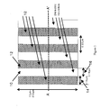
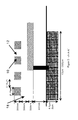
- An embodiment of such a sensor is illustrated in Figs. 1 and 2.
- CMOS complementary metal-oxide-semiconductor
- transistor gates for example, 0.35 ⁇ m, 0.18 ⁇ m, or 0.13 ⁇ m.
- metal interconnects have also reduced in size, for example, 0.5 ⁇ m, 0.32 ⁇ m, or 0.16 ⁇ m.
- the wavelength of light in air is between 0.45 ⁇ m and 0.65 ⁇ m. As the sizes of these metal structures is less than the wavelength of light, they are therefore suitable for diffractive-type optics.
- a polarizing assembly 10 according to a first embodiment of the present invention is shown in Figs. 1 and 2.
- An array of parallel metal lines 12 is provided having a width 14 of 0.16 ⁇ m, and are spaced apart by a spacing 16 of 0.16 ⁇ m.
- a pitch of the grid is defined as the summed width of the width 14 of one metal line and the spacing 16 adjacent to that line.
- the pitch of the illustrated array is 0.32 ⁇ m.
- the metal lines 12 are formed directly on a dielectric layer 18 of a silicon photodetector.
- the image sensor produced comprises an integrated photodetector and polarising assembly.
- integrated is taken to mean that the polarising assembly is immovably attached in a fixed spatial relationship to a photodetector.
- the illustrated array will allow approximately 50% of incident radiation to pass therethrough. It will be appreciated that the pitch can be varied by choosing different values of one or both of the width 14 of the metal lines 12 or the spacing 16 of the metal lines 12, in order to allow different proportions of incident light to pass through the array, as required.
- any metal can be chosen, as long as it has a conductivity suitable to act effectively in an array as a polariser of incident light.
- a pitch of very much greater than 30nm can be used to provide a polarizing effect which is useful for production of a polarization sensitive image sensor.
- "very much greater" than a particular figure means that the pitch must be at least twice that particular figure.
- the pitch is approximately ten times the particular figure, i.e. over 300nm. The minimum allowable pitch will be governed by the manufacturing process.
- the polarising structure can formed on the surface of any type of silicon photodetector, but one of high sensitivity is preferred as the polarisor introduces a significant attenuation. For example, in the embodiment illustrated in Fig. 2, at least 50% of incident light is lost.
- LTF converters are product numbers TSL235, TSL245 and similar devices available from Texas Advanced Optoelectronic Solutions. These include a photodiode and a current to frequency converter integrated on the same CMOS IC.
- LTF converters are particularly useful for the present application because they employ a charge sensing technique. This permits the use of large area photodetectors, which collect more photons but have a large capacitance. More conventional readout techniques (e.g. 3 transistor) use a voltage sensing technique, so the large capacitance of the photodetector (the capacitance is proportional to its area) effectively cancels out the advantage of the greater number of photons collected by the larger area.
- Fig. 3 illustrates a charge sensing amplifier that uses an operation amplifier 20 with a feedback capacitor, Cfb 22.
- the amplifier 20 has a very high input impedance and so no current flows into it.
- the output will change so that the inverting input remains at the same potential as the non-inverting input. In doing so, a current will flow through the feedback capacitor Cfb 22. This will be of exactly the same magnitude (but opposite sign) to the photocurrent Ipd.
- Vout -Ipd x Tint/Cfb (equation 1), and so the output voltage is independent of the pixel's capacitance.
- the architecture is very suitable for large photodiodes.
- the disadvantage is that the charge amplifier 20 needs to be reset periodically as the output voltage will swing outside the operating range of the amplifier 20, as shown in Fig. 4.
- This reset can be achieved as part of a system's AEC (automatic exposure control).
- a practical method for resetting the charge-amp's feedback capacitor 22 is shown in Fig. 5, the readout signals from which are illustrated in Fig. 6.
- Equation 2 the slope of the charge-amplifier's 20 output is proportional to the light. Hence the frequency of the light to frequency conversion is also proportional to the light.
- Fout Ipd/(2 x Cfb x (Vthreshold - Vrt)) (equation 2).
- the above concepts can be applied in a manufacturing process to form a polarising structure on selected portions of an image sensor. These portions may or may not cover the entire image sensing surface. Furthermore, the orientation of the lines that are formed can be predetermined and can be different for different portions of the image sensor, so that different polarisations can be detected.
- This polarisation sensitive image sensor can be incorporated in a number of different products, which include but are not limited to, a chip or integrated circuit, an optical mouse, and a digital camera provided as a separate unit or as part of a mobile telephone or webcam.
- an image sensor made in accordance with the principles of the invention may be incorporated in a product together with a non-polarized detector to gather information about ambient light.
Landscapes
- Physics & Mathematics (AREA)
- General Physics & Mathematics (AREA)
- Spectroscopy & Molecular Physics (AREA)
- Optics & Photonics (AREA)
- Solid State Image Pick-Up Elements (AREA)
Abstract
Description
Claims (17)
- A polarization sensitive solid state image sensor comprising an integrated photodetector and polarizing assembly (10).
- The image sensor of claim 1, wherein the polarizing assembly comprises two or more regions which among them have two or more different polarisations.
- The image sensor of claim 1 or claim 2, wherein the polarizing assembly comprises a plurality of parallel metal lines (12).
- The image sensor of claim 3, wherein the metal lines (12) have a pitch of a value less than a wavelength in the spectral range of visible light.
- The image sensor of claim 4, wherein the pitch is very much greater than 30nm.
- The image sensor of any of claims 3 to 5, wherein the parallel lines (12) are spaced apart by a distance (16) equal to their width (14).
- The image sensor of any preceding claim, wherein the photodetector comprises a charge amplifier (20).
- The image sensor of claim 7, wherein the photodetector comprises a light to frequency converter.
- The image sensor of any preceding claim, wherein the polarizing assembly (10) is formed on a dielectric material (18) which is itself formed on the photodetector.
- An integrated circuit comprising the image sensor of any of claims 1 to 9.
- An optical mouse comprising the image sensor of any of claims 1 to 9.
- A digital camera comprising the image sensor of any of claims 1 to 9.
- A mobile telephone comprising the digital camera of claim 12.
- A method of forming a polarization sensitive solid state image sensor comprising the step of forming an integrated photodetector and polarizing assembly (10).
- The method of claim 14, wherein the polarizing assembly comprises two or more regions which among them have two or more different polarisations.
- The method of claim 14 or claim 15, comprising the step of forming a photodetector having an upper dielectric layer (18) and forming the polarizing assembly upon the dielectric layer (18).
- The method of any of claims 14-16, comprising the step of forming a plurality of parallel metal lines (12) by a lithographic or etching process.
Priority Applications (3)
| Application Number | Priority Date | Filing Date | Title |
|---|---|---|---|
| EP04253649A EP1607773B1 (en) | 2004-06-18 | 2004-06-18 | Polarization sensitive solid state image sensor |
| DE602004019888T DE602004019888D1 (en) | 2004-06-18 | 2004-06-18 | Polarization-sensitive solid-state image sensor |
| US11/154,330 US7186968B2 (en) | 2004-06-18 | 2005-06-16 | Polarization sensitive solid state image sensor including integrated photodetector and polarizing assembly and associated methods |
Applications Claiming Priority (1)
| Application Number | Priority Date | Filing Date | Title |
|---|---|---|---|
| EP04253649A EP1607773B1 (en) | 2004-06-18 | 2004-06-18 | Polarization sensitive solid state image sensor |
Publications (2)
| Publication Number | Publication Date |
|---|---|
| EP1607773A1 true EP1607773A1 (en) | 2005-12-21 |
| EP1607773B1 EP1607773B1 (en) | 2009-03-11 |
Family
ID=34930417
Family Applications (1)
| Application Number | Title | Priority Date | Filing Date |
|---|---|---|---|
| EP04253649A Expired - Lifetime EP1607773B1 (en) | 2004-06-18 | 2004-06-18 | Polarization sensitive solid state image sensor |
Country Status (3)
| Country | Link |
|---|---|
| US (1) | US7186968B2 (en) |
| EP (1) | EP1607773B1 (en) |
| DE (1) | DE602004019888D1 (en) |
Cited By (1)
| Publication number | Priority date | Publication date | Assignee | Title |
|---|---|---|---|---|
| WO2009154713A1 (en) * | 2008-06-19 | 2009-12-23 | Eastman Kodak Company | High dynamic range image sensor |
Families Citing this family (16)
| Publication number | Priority date | Publication date | Assignee | Title |
|---|---|---|---|---|
| US7550701B2 (en) * | 2003-02-25 | 2009-06-23 | Omnivision Cdm Optics, Inc. | Non-linear wavefront coding systems and methods |
| US7453653B2 (en) * | 2004-09-14 | 2008-11-18 | Omnivision Cdm Optics, Inc. | Low height imaging system and associated methods |
| US20070244377A1 (en) * | 2006-03-14 | 2007-10-18 | Cozad Jenny L | Pulse oximeter sleeve |
| WO2007134062A2 (en) * | 2006-05-08 | 2007-11-22 | Slicex, Inc. | Sensing light and sensing the state of a memory cell |
| US20090109427A1 (en) * | 2007-10-31 | 2009-04-30 | Ng Mei Yee | Conversion Of Properties Of Light To Frequency Counting |
| US9307063B2 (en) * | 2008-01-23 | 2016-04-05 | Lexmark International, Inc. | Camera cell phone with integrated wireless mouse |
| DE102008014334B4 (en) | 2008-03-14 | 2009-12-17 | Fraunhofer-Gesellschaft zur Förderung der angewandten Forschung e.V. | Integrated polarization sensor |
| US8771204B2 (en) * | 2008-12-30 | 2014-07-08 | Masimo Corporation | Acoustic sensor assembly |
| US8238026B1 (en) | 2009-02-03 | 2012-08-07 | Sandia Corporation | Polarization-sensitive infrared image sensor including a plurality of optical fibers |
| US20130133701A1 (en) * | 2011-11-28 | 2013-05-30 | Intermolecular, Inc. | Method and apparatus for dispensing an inert gas |
| US8881983B2 (en) | 2011-12-13 | 2014-11-11 | Honeywell International Inc. | Optical readers and methods employing polarization sensing of light from decodable indicia |
| WO2013158975A1 (en) * | 2012-04-20 | 2013-10-24 | Washington University | Sensor for spectral-polarization imaging |
| US9234836B2 (en) * | 2012-11-15 | 2016-01-12 | Fraunhofer-Gesellschaft Zur Foerderung Der Angewandten Forschung E.V. | Measurement of a fiber direction of a carbon fiber material and fabrication of an object in carbon fiber composite technique |
| DE102015200324A1 (en) | 2015-01-13 | 2016-07-14 | Fraunhofer-Gesellschaft zur Förderung der angewandten Forschung e.V. | Polarizing filter with metallic bars |
| WO2020021311A1 (en) | 2018-07-23 | 2020-01-30 | Bosch Car Multimedia Portugal S.a. | Terrestrial vehicle range finder device and operation method thereof |
| US10659751B1 (en) | 2018-12-14 | 2020-05-19 | Lyft Inc. | Multichannel, multi-polarization imaging for improved perception |
Family Cites Families (7)
| Publication number | Priority date | Publication date | Assignee | Title |
|---|---|---|---|---|
| US5963333A (en) * | 1996-09-12 | 1999-10-05 | Color Savvy Systems Limited | Color sensor |
| US6108131A (en) * | 1998-05-14 | 2000-08-22 | Moxtek | Polarizer apparatus for producing a generally polarized beam of light |
| US20020167727A1 (en) * | 2001-03-27 | 2002-11-14 | Hansen Douglas P. | Patterned wire grid polarizer and method of use |
| US6665119B1 (en) * | 2002-10-15 | 2003-12-16 | Eastman Kodak Company | Wire grid polarizer |
| US7113335B2 (en) * | 2002-12-30 | 2006-09-26 | Sales Tasso R | Grid polarizer with suppressed reflectivity |
| EP1597616A4 (en) * | 2003-02-10 | 2008-04-09 | Nanoopto Corp | UNIVERSAL BROADBAND POLARIZER, DEVICES COMPRISING THE POLARIZER, AND METHOD FOR MANUFACTURING THE POLARIZER |
| US20040174596A1 (en) * | 2003-03-05 | 2004-09-09 | Ricoh Optical Industries Co., Ltd. | Polarization optical device and manufacturing method therefor |
-
2004
- 2004-06-18 EP EP04253649A patent/EP1607773B1/en not_active Expired - Lifetime
- 2004-06-18 DE DE602004019888T patent/DE602004019888D1/en not_active Expired - Lifetime
-
2005
- 2005-06-16 US US11/154,330 patent/US7186968B2/en not_active Expired - Lifetime
Non-Patent Citations (7)
| Title |
|---|
| BERLIEN C J A-J ET AL: "A MONOLITHIC LIGHT-TO-FREQUENCY CONVERTER WITH A SCALABLE SENSOR ARRAY", 1 February 1994, IEEE INTERNATIONAL SOLID STATE CIRCUITS CONFERENCE, IEEE INC. NEW YORK, US, PAGE(S) 158-159,329, ISSN: 0193-6530, XP000507099 * |
| CHEN E ET AL: "A NOVEL DEVICE FOR DETECTING THE POLARIZATION DIRECTION OF LINEAR POLARIZED LIGHT USING INTEGRATED SUBWAVELENGTH GRATINGS AND PHOTODETECTORS", IEEE PHOTONICS TECHNOLOGY LETTERS, IEEE INC. NEW YORK, US, vol. 9, no. 9, September 1997 (1997-09-01), pages 1259 - 1261, XP000721228, ISSN: 1041-1135 * |
| CHEN ET AL.: "IEEE Photonics Technology Letters", vol. 9, September 1997, IEEE INC., article "A novel device for detecting the polarization direction of linear polarized light using integrated subwavelength gratings and photodetectors", pages: 1259 - 1261 |
| DE GRAAF G ET AL: "Light-to-frequency converter using integrating mode photodiodes", 4 June 1996, INSTRUMENTATION AND MEASUREMENT TECHNOLOGY CONFERENCE, 1996. IMTC-96. CONFERENCE PROCEEEDINGS. QUALITY MEASUREMENTS: THE INDISPENSABLE BRIDGE BETWEEN THEORY AND REALITY., IEEE BRUSSELS, BELGIUM 4-6 JUNE 1996, NEW YORK, NY, USA,IEEE, US, PAGE(S) 1072-, ISBN: 0-7803-3312-8, XP010164037 * |
| DOUMUKI T ET AL.: "An aluminum-wire grid polarizer fabricated on a gallium- arsenide photodiode", APPLIED PHYSICS LETTERS, AMERICAN INSTITUTE OF PHYSICS, NEW YORK, US, vol. 71, no. 5, 4 August 1997 (1997-08-04), pages 686 - 688 |
| DOUMUKI T ET AL: "AN ALUMINUM-WIRE GRID POLARIZER FABRICATED ON A GALLIUM-ARSENIDE PHOTODIODE", APPLIED PHYSICS LETTERS, AMERICAN INSTITUTE OF PHYSICS. NEW YORK, US, vol. 71, no. 5, 4 August 1997 (1997-08-04), pages 686 - 688, XP000699633, ISSN: 0003-6951 * |
| SCHNABEL B ET AL: "STUDY ON POLARIZING VISIBLE LIGHT BY SUBWAVELENGTH-PERIOD METAL-STRIPE GRATINGS", OPTICAL ENGINEERING, SOC. OF PHOTO-OPTICAL INSTRUMENTATION ENGINEERS. BELLINGHAM, US, vol. 38, no. 2, February 1999 (1999-02-01), pages 220 - 226, XP000955101, ISSN: 0091-3286 * |
Cited By (2)
| Publication number | Priority date | Publication date | Assignee | Title |
|---|---|---|---|---|
| WO2009154713A1 (en) * | 2008-06-19 | 2009-12-23 | Eastman Kodak Company | High dynamic range image sensor |
| US7964840B2 (en) | 2008-06-19 | 2011-06-21 | Omnivision Technologies, Inc. | High dynamic range image sensor including polarizer and microlens |
Also Published As
| Publication number | Publication date |
|---|---|
| US7186968B2 (en) | 2007-03-06 |
| EP1607773B1 (en) | 2009-03-11 |
| DE602004019888D1 (en) | 2009-04-23 |
| US20050279921A1 (en) | 2005-12-22 |
Similar Documents
| Publication | Publication Date | Title |
|---|---|---|
| US7186968B2 (en) | Polarization sensitive solid state image sensor including integrated photodetector and polarizing assembly and associated methods | |
| US9219090B2 (en) | Solid-state image capturing device and electronic device | |
| CN113572990B (en) | Hybrid CMOS Image Sensor with Event-Driven Sensing | |
| KR100801181B1 (en) | Digital image sensor and its design method | |
| US7545423B2 (en) | Image sensor having a passivation layer exposing at least a main pixel array region and methods of fabricating the same | |
| KR102638779B1 (en) | Image sensor | |
| US20050133879A1 (en) | Solid-state imaging device, signal processing device, camera, and spectral device | |
| US9812604B2 (en) | Photosensing device with graphene | |
| KR101660943B1 (en) | Near-infrared photodetector and image sensor employing the same and manufacturing method thereof | |
| US20120242621A1 (en) | Image sensor and display device incorporating the same | |
| KR100826407B1 (en) | UV light-receiving photodiode and image sensor comprising the same | |
| WO2008027412A2 (en) | Method and apparatus to improve filter characteristics of optical filters | |
| WO2004047180A1 (en) | Photo detection device | |
| US11303840B1 (en) | Image sensor and sensing method thereof with polarizers for removing background noise | |
| CN107924925A (en) | Optical sensor with narrow angular response | |
| TWI603463B (en) | Light sensor and light sensing module | |
| US8952310B2 (en) | Plasmonic light sensors | |
| Knipp et al. | Vertically integrated amorphous silicon color sensor arrays | |
| US11796386B2 (en) | Optical sensor and apparatus comprising an optical sensor having a readout circuit to determine an ambient light level based on voltage across a photodetector at the end of an exposure time | |
| JP5533294B2 (en) | Image sensor and imaging apparatus | |
| CN112909036A (en) | Light sensing system and light sensor with polarizer | |
| JP3691176B2 (en) | Semiconductor energy detector | |
| US7807996B2 (en) | Test pattern of CMOS image sensor and method of measuring process management using the same | |
| Gross | Sensor technology and signal processing | |
| CN118825045A (en) | Pixel unit and imaging system |
Legal Events
| Date | Code | Title | Description |
|---|---|---|---|
| PUAI | Public reference made under article 153(3) epc to a published international application that has entered the european phase |
Free format text: ORIGINAL CODE: 0009012 |
|
| AK | Designated contracting states |
Kind code of ref document: A1 Designated state(s): AT BE BG CH CY CZ DE DK EE ES FI FR GB GR HU IE IT LI LU MC NL PL PT RO SE SI SK TR |
|
| AX | Request for extension of the european patent |
Extension state: AL HR LT LV MK |
|
| 17P | Request for examination filed |
Effective date: 20060607 |
|
| 17Q | First examination report despatched |
Effective date: 20060703 |
|
| AKX | Designation fees paid |
Designated state(s): DE FR GB IT |
|
| 17Q | First examination report despatched |
Effective date: 20060703 |
|
| GRAP | Despatch of communication of intention to grant a patent |
Free format text: ORIGINAL CODE: EPIDOSNIGR1 |
|
| RAP1 | Party data changed (applicant data changed or rights of an application transferred) |
Owner name: STMICROELECTRONICS (RESEARCH & DEVELOPMENT) LIMITE |
|
| GRAS | Grant fee paid |
Free format text: ORIGINAL CODE: EPIDOSNIGR3 |
|
| GRAA | (expected) grant |
Free format text: ORIGINAL CODE: 0009210 |
|
| AK | Designated contracting states |
Kind code of ref document: B1 Designated state(s): DE FR GB IT |
|
| REG | Reference to a national code |
Ref country code: GB Ref legal event code: FG4D |
|
| REF | Corresponds to: |
Ref document number: 602004019888 Country of ref document: DE Date of ref document: 20090423 Kind code of ref document: P |
|
| PLBE | No opposition filed within time limit |
Free format text: ORIGINAL CODE: 0009261 |
|
| STAA | Information on the status of an ep patent application or granted ep patent |
Free format text: STATUS: NO OPPOSITION FILED WITHIN TIME LIMIT |
|
| 26N | No opposition filed |
Effective date: 20091214 |
|
| PG25 | Lapsed in a contracting state [announced via postgrant information from national office to epo] |
Ref country code: IT Free format text: LAPSE BECAUSE OF FAILURE TO SUBMIT A TRANSLATION OF THE DESCRIPTION OR TO PAY THE FEE WITHIN THE PRESCRIBED TIME-LIMIT Effective date: 20090311 |
|
| REG | Reference to a national code |
Ref country code: DE Ref legal event code: R082 Ref document number: 602004019888 Country of ref document: DE Representative=s name: MURGITROYD & COMPANY, DE |
|
| REG | Reference to a national code |
Ref country code: FR Ref legal event code: TP Owner name: SK HYNIX INC., KR Effective date: 20150316 |
|
| REG | Reference to a national code |
Ref country code: DE Ref legal event code: R082 Ref document number: 602004019888 Country of ref document: DE Representative=s name: MURGITROYD & COMPANY, DE Effective date: 20150325 Ref country code: DE Ref legal event code: R081 Ref document number: 602004019888 Country of ref document: DE Owner name: SK HYNIX INC., ICHEON, KR Free format text: FORMER OWNER: STMICROELECTRONICS (RESEARCH & DEVELOPMENT) LTD., MARLOW, BUCKINGHAMSHIRE, GB Effective date: 20150325 |
|
| REG | Reference to a national code |
Ref country code: GB Ref legal event code: 732E Free format text: REGISTERED BETWEEN 20150416 AND 20150422 |
|
| REG | Reference to a national code |
Ref country code: GB Ref legal event code: 732E Free format text: REGISTERED BETWEEN 20150423 AND 20150430 |
|
| REG | Reference to a national code |
Ref country code: FR Ref legal event code: PLFP Year of fee payment: 13 |
|
| REG | Reference to a national code |
Ref country code: FR Ref legal event code: PLFP Year of fee payment: 14 |
|
| REG | Reference to a national code |
Ref country code: FR Ref legal event code: PLFP Year of fee payment: 15 |
|
| PGFP | Annual fee paid to national office [announced via postgrant information from national office to epo] |
Ref country code: GB Payment date: 20220506 Year of fee payment: 19 Ref country code: FR Payment date: 20220512 Year of fee payment: 19 Ref country code: DE Payment date: 20220506 Year of fee payment: 19 |
|
| REG | Reference to a national code |
Ref country code: DE Ref legal event code: R119 Ref document number: 602004019888 Country of ref document: DE |
|
| GBPC | Gb: european patent ceased through non-payment of renewal fee |
Effective date: 20230618 |
|
| PG25 | Lapsed in a contracting state [announced via postgrant information from national office to epo] |
Ref country code: DE Free format text: LAPSE BECAUSE OF NON-PAYMENT OF DUE FEES Effective date: 20240103 Ref country code: GB Free format text: LAPSE BECAUSE OF NON-PAYMENT OF DUE FEES Effective date: 20230618 |
|
| PG25 | Lapsed in a contracting state [announced via postgrant information from national office to epo] |
Ref country code: FR Free format text: LAPSE BECAUSE OF NON-PAYMENT OF DUE FEES Effective date: 20230630 |