EP1605589A1 - Matching circuit - Google Patents
Matching circuit Download PDFInfo
- Publication number
- EP1605589A1 EP1605589A1 EP04720743A EP04720743A EP1605589A1 EP 1605589 A1 EP1605589 A1 EP 1605589A1 EP 04720743 A EP04720743 A EP 04720743A EP 04720743 A EP04720743 A EP 04720743A EP 1605589 A1 EP1605589 A1 EP 1605589A1
- Authority
- EP
- European Patent Office
- Prior art keywords
- matching
- block
- matching block
- parallel
- series
- Prior art date
- Legal status (The legal status is an assumption and is not a legal conclusion. Google has not performed a legal analysis and makes no representation as to the accuracy of the status listed.)
- Withdrawn
Links
Images












Classifications
-
- H—ELECTRICITY
- H03—ELECTRONIC CIRCUITRY
- H03H—IMPEDANCE NETWORKS, e.g. RESONANT CIRCUITS; RESONATORS
- H03H7/00—Multiple-port networks comprising only passive electrical elements as network components
- H03H7/38—Impedance-matching networks
- H03H7/383—Impedance-matching networks comprising distributed impedance elements together with lumped impedance elements
-
- H—ELECTRICITY
- H01—ELECTRIC ELEMENTS
- H01P—WAVEGUIDES; RESONATORS, LINES, OR OTHER DEVICES OF THE WAVEGUIDE TYPE
- H01P5/00—Coupling devices of the waveguide type
- H01P5/02—Coupling devices of the waveguide type with invariable factor of coupling
-
- H—ELECTRICITY
- H03—ELECTRONIC CIRCUITRY
- H03F—AMPLIFIERS
- H03F1/00—Details of amplifiers with only discharge tubes, only semiconductor devices or only unspecified devices as amplifying elements
- H03F1/56—Modifications of input or output impedances, not otherwise provided for
-
- H—ELECTRICITY
- H04—ELECTRIC COMMUNICATION TECHNIQUE
- H04B—TRANSMISSION
- H04B1/00—Details of transmission systems, not covered by a single one of groups H04B3/00 - H04B13/00; Details of transmission systems not characterised by the medium used for transmission
- H04B1/005—Details of transmission systems, not covered by a single one of groups H04B3/00 - H04B13/00; Details of transmission systems not characterised by the medium used for transmission adapting radio receivers, transmitters andtransceivers for operation on two or more bands, i.e. frequency ranges
- H04B1/0067—Details of transmission systems, not covered by a single one of groups H04B3/00 - H04B13/00; Details of transmission systems not characterised by the medium used for transmission adapting radio receivers, transmitters andtransceivers for operation on two or more bands, i.e. frequency ranges with one or more circuit blocks in common for different bands
-
- H—ELECTRICITY
- H04—ELECTRIC COMMUNICATION TECHNIQUE
- H04B—TRANSMISSION
- H04B1/00—Details of transmission systems, not covered by a single one of groups H04B3/00 - H04B13/00; Details of transmission systems not characterised by the medium used for transmission
- H04B1/02—Transmitters
- H04B1/04—Circuits
- H04B1/0458—Arrangements for matching and coupling between power amplifier and antenna or between amplifying stages
-
- H—ELECTRICITY
- H03—ELECTRONIC CIRCUITRY
- H03F—AMPLIFIERS
- H03F2200/00—Indexing scheme relating to amplifiers
- H03F2200/111—Indexing scheme relating to amplifiers the amplifier being a dual or triple band amplifier, e.g. 900 and 1800 MHz, e.g. switched or not switched, simultaneously or not
Definitions
- the present invention relates to a matching circuit, and more particularly, to a multi-band matching circuit applicable to establishing matching among circuits having different impedances in a plurality of frequency bands, and further, to a matching circuit preferably applicable to constructing a small multi-band high-efficiency power amplifier which efficiently amplifies signals of a plurality of frequency bands used in communication equipment such as a mobile communication and satellite communication terminal.
- a radio set With diversification of services provided by radio communications, a radio set is required to operate in a plurality of frequency bands and, therefore, is expected to be available for some signals whose center frequencies are different individually.
- One of indispensable apparatuses included in a radio set is a power amplifier.
- a power amplifier In order to realize efficient amplification, it is necessary to establish impedance matching between an amplification element and circuits peripheral thereto and a matching circuit is used.
- a conventional multi-band power amplifier for example, an amplifier used in a "multi-band mobile station" is disclosed in "Mobile Station” (by Koji Chiba et al., NTT DoCoMo Technical Journal, Vol.10, No.1).
- the power amplifier in Fig. 1 is constructed of an input switch 11, an 800 MHz band amplifier 21, a 1.5 GHz band amplifier 22 and an output switch 12.
- a transmit signal converted to a radio frequency is selectively supplied to either the amplifier 21 or 22 designed for each frequency band by the input switch 11, amplified and then supplied to an antenna through the output switch 12.
- each amplifier 21, 22 is constructed of an input side matching circuit 25, an amplification element 26 and an output side matching circuit 27. Both matching circuits 25, 27 are designed to establish impedance matching between a signal source 23 and amplification element and between the amplification element 26 and a load 28 for the frequency band of an input signal, respectively.
- the input/output impedance of the amplification element 26 generally differs from one frequency to another and when signals of different frequency bands are amplified, the input side and output side require matching circuits designed for their respective bands.
- amplifying signals of two bands requires two lines of amplifiers each made up of the input side matching circuit 25, amplification element 26 and output side matching circuit 27 as shown in Fig.
- the mounting area becomes substantially double. Moreover, when signals having more bands are amplified, the mounting area becomes as many times as lines of amplifiers. When the number of amplification elements 26 increases, power consumption of the entire amplifier may increase and stability of the circuit may be lost. Furthermore, this is problematic because the matching circuit accounts for a large proportion of the mounting area of the amplifier. Furthermore, when the number of lines of amplifiers is increased, an SPnT (Single Pole n Throw) switch is required as the input/output switch, but the SPnT switch has a very complicated structure and is difficult to manufacture. Using the SPnT switch also involves a problem that switch insertion loss increases in proportion to the number of lines of amplifiers.
- SPnT Single Pole n Throw
- FIG. 3 shows the structure of a high-efficiency power amplifier, which uses an input side matching circuit 25, an amplification element 26, an output side matching circuit 27 and a harmonics control circuit 24.
- the harmonics control circuit 24 controls the harmonics under a load condition, for example, under which all the even-harmonics are short-circuited and all the odd-order harmonics are left open. When this termination condition is set, it is possible to obtain maximum efficiency of 100% in theory.
- harmonics control circuit 24 is not limited to this design method.
- a conventional two-band high-efficiency power amplifier is provided with two lines of the input side matching circuits 25, amplification elements 26, harmonics control circuits 24, output side matching circuits 27 which are optimized in each frequency band and used by selecting the line using SPDT switches, that is, Single Pole Double Throw switches 11, 12 as shown in Fig. 1.
- the conventional example of the multi-band high-efficiency power amplifier has a problem that the overall circuit area increases as the number of the operating bands increases for the above described reason.
- amplifying signals of n bands requires n lines of matching circuits, n lines of harmonics control circuits and n lines of amplification elements, and the circuit area becomes approximately n-fold.
- This is especially problematic because the matching circuit and harmonics control circuit are the circuits which account for a large proportion of the circuit area of the amplifier.
- adopting a multi-line amplifier requires the SPnT (Single Pole n Throw) switch as the input/output switch and this SPnT switch has a complicated structure, it is difficult to manufacture a high performance switch and an increase in the number of lines may increase switch insertion losses.
- an insertion loss may cause a reduction of efficiency and cause difficulty especially when used for a cellular phone.
- a method using a wideband design may also be used to implement a multi-band matching circuit.
- the available band of a circuit becomes wider, the number of elements constituting a matching circuit increases, which reduces the gain and efficiency compared to a narrow-band design. Therefore, in view of application to a power amplifier in particular, the use of the wideband design results in upsizing of the apparatus and deterioration of the performance.
- the matching circuit includes a main matching block inserted in a signal path, with matching established in at least a first frequency band, a series matching block inserted in the signal path, one end of which is connected to the main matching block, with matching to the main matching block established in the first frequency band and a series connection between a parallel matching block and a switch, in which one end of the series connection is connected to the signal path at the other end of the series matching block and setting the switch to ON/OFF realizes selective matching in the first frequency band and a second frequency band which is different from the first frequency band.
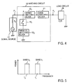
- Fig. 4 illustrates an embodiment of a matching circuit according to the present invention.
- This matching circuit 50 is a circuit that matches an impedance of a load circuit 28 connected to a port P 2 to an impedance Z s of a signal source 23 connected to a port P 1 and operates, for example, as a matching circuit for signals of two frequency band b 1 and b 2 having center frequencies of f 1 and f 2 shown in Fig. 5.
- the impedance of the signal source 23 is assumed to be Z s regardless of the frequency. Since the impedance of the load circuit 28 depends on the frequency, it is expressed as Z L (f).
- This matching circuit 50 is made up of a series matching block 52 2 and a main matching block 51 inserted in series in the signal path between the ports P 1 and P 2 , and a series connection of a parallel matching block 53 2 and a switch 54 2 inserted between an end of the series matching block 52 2 on the port P 1 side and a ground.
- the parallel matching block 53 2 is connected to the signal path via the switch 54 2 .
- the series matching block 52 2 is inserted in series to the load circuit 28 and the parallel matching block 53 2 is inserted in parallel to the load circuit 28 when the switch 54 2 is ON.
- the main matching block 51 in Fig. 4 is the circuit which matches the impedance Z L (f 1 ) of the port P 2 to the input impedance Z s seen looking into the signal source 23 from the port P 1 , at the frequency f 1 .
- the series matching block 52 2 is constructed of a transmission line, etc., whose characteristic impedance is equal to Z s at the frequency f 1 so as not to influence signal transmission of the signal of the frequency f 1 between connection points A and B in Fig. 4.
- the main matching block 51 establishes impedance matching between the port P 1 and port P 2 at the frequency f 1 .
- the main matching block 51 is designed to operate as a matching circuit at the frequency f 1 .
- the main matching block 51 simply operates as an impedance converter at the frequency f 2 . Therefore, the impedance Z L (f 2 ) of the port P 2 is converted to an arbitrary impedance Z L '(f 2 ) by the main matching block 51 for the signal of frequency f 2 .
- the switch 54 2 when the switch 54 2 is set to ON, it is possible to establish matching between the load impedance Z L '(f 2 ) and the impedance Z s of the port P 1 by presetting the impedances of the series matching block 52 2 and the parallel matching block 53 2 connected in parallel to the series matching block 52 2 at the frequency f 2 as appropriate. That is, it is possible to design the matching circuit 50 for the frequency f 2 no matter what structure the main matching block 51 may have. Therefore, by adding the parallel matching block 53 2 to the main matching block 51 using the switch 54 2 , it is possible to change the overall matching circuit 50 to a matching circuit for the input signal of the frequency f 2 .
- the matching circuit 50 so as to selectively respond to each signal with different frequency bands individually by changing the state (ON/OFF) of one switch 54 2 .
- the other end of the parallel matching block 53 2 is grounded, but the parallel matching block 53 2 may also be constructed of an open-end line.
- the main matching block 51 can be constructed in various configurations as will be explained below and the same will apply to other embodiments.
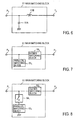
- a first example of the structure of this main matching block 51 will be explained with reference to Fig. 6.
- the main matching block 51 shown here is made up of an inductive lumped element 51B and a capacitive lumped element 51A. Combining a plurality of lumped elements in this way makes it possible to construct a matching circuit of an arbitrary frequency f.
- the main matching block 51 illustrated is made up of a series matching block 52 1 and a parallel matching block 53 1 whose one end is connected to the input side of the series matching block 52 1 .
- the series matching block 52 1 may be a delay circuit made up of, for example, a lumped element or also made up of a transmission line whose characteristic impedance is equal to Z s .
- a matching circuit of an arbitrary frequency f can be constructed of such a lumped element or transmission line.
- the parallel matching block 53 1 may be made up of, for example, an open-end line or may also be made up of an end short-circuited line.
- the main matching block 51 illustrated is made up of a series matching block 51 1 and a parallel matching block 53 1 , one end of which is connected to the input side of the series matching block 52 1 through a switch 54 1 and the other end of which is grounded.
- the switch 54 1 When the switch 54 1 is ON, an arbitrary impedance of a port P 2 can be matched to the impedance of a port P 3 by the series matching block 51 1 and the parallel matching block 53 1 , and therefore it is possible to design a matching circuit for a signal of an arbitrary frequency.
- the switch 54 1 when the switch 54 1 is OFF, the signal passes through only the series matching block 51 1 in the main matching block 51 and the parallel matching block 53 1 does not contribute to impedance conversion. Therefore, the main matching block 51 changes the impedance of the port P 2 only by an amount of impedance conversion by the series matching block 51 1 .
- Fig. 9 shows a second embodiment of the matching circuit 50.
- This embodiment assumes a case where the impedance of a signal source 23 has a frequency characteristic such as an FET does and the impedance Z L of a load circuit 28 is constant at various frequencies.
- This embodiment has the structure of the embodiment of the matching circuit 50 shown in Fig. 4 with the positions of the main matching block 51 and the series matching block 52 2 between the ports P 1 and P 2 switched round so that the main matching block 51 is located closer to the signal source 23 which has a frequency characteristic and with the parallel matching block 53 2 connected to the port P 2 side through the switch 54 2 .
- the principle of operation is the same as that in Fig. 4 and explanations thereof will be omitted.
- Fig. 10 shows a third embodiment of the matching circuit 50 of the present invention.
- the embodiment in Fig. 10 is provided with a cascade connection of (N-1) stages (N is an integer of 3 or greater in this embodiment), each stage having a combination similar to that of a series matching block 52 2 , a parallel matching block 53 2 and a switch 54 2 so as to operate as a matching circuit for signals of N frequency bands b 1 to b N shown in Fig. 11.
- the embodiment in Fig. 10 corresponds to an expansion of the embodiment in Fig.
- nth switch 54 n setting the nth (n: integer of 2 to N) switch 54 n to ON, it is possible to change the entire matching circuit 50 to a matching circuit for an input signal of a center frequency f n with the corresponding nth parallel matching block 53 n connected in parallel, series matching blocks 52 2 to 52 N and main matching block 51.
- the matching circuit 50 operates as a matching circuit of a frequency f 3 . Furthermore, when the switch 54 2 is closed and the switch 54 3 is also closed, the matching circuit 50 operates as a matching circuit of a frequency f 4 corresponding to the case where the parallel matching blocks 53 2 and 53 3 are selected.
- the number of cascade connection stages is increased, it is possible to increase the number of frequency bands which can be matched up to a maximum number of combinations of switches which are closed simultaneously in principle. In the embodiment in Fig. 10, one end of each of the parallel matching block 53 2 to 53 N is grounded, but when the parallel matching blocks are constructed using open-end lines, they need not always be grounded.
- the matching circuit shown in Fig. 12 can also operate in plural bands using wideband matching circuits constructed by closing a plurality of switches 53 2 , 53 3 simultaneously.
- Fig. 13 illustrates a fourth embodiment of the matching circuit of the present invention.
- a 1-input N-output switch (single pole N throw switch) SW1 connected to a port P 1 and a N-input 1-output switch (single pole N throw switch) SW2 whose output side is connected to the main matching block 51 are provided and a directly connected line 58 1 having a characteristic impedance Z s and (N-1) matching blocks 59 2 to 59 N are connected to N input/output terminals between the switches SW1, SW2 in a selectable manner.
- the embodiment in Fig. 13 as well as the embodiment in Fig. 10 operates as the matching circuit 50 for signals of the N frequency bands shown in Fig. 11.
- the main matching block 51 is a matching circuit for an input signal of a frequency f 1 .
- the two switches that is, 1-input N-output switch SW1 and N-input 1-output switch SW2 are switched to the first output and the first input, and the port P 1 and port P 2 are connected through the directly connected line 58 1 .
- the 1-input N-output switch SW1 and N-input 1-output switch SW2 are switched to the switch contacts corresponding to the matching block 59 n and controlled.
- the switches 52 for example shown in Fig. 10
- Fig. 14 shows an example of the structure which allows the entire parallel matching block 53 to be used in more frequency bands by constructing one or an arbitrary number of parallel matching blocks (represented by the parallel block 53) in the matching circuit 50 shown in Figs. 4, 9, 10, 12 with sub-matching circuits having a reactance, respectively.
- This parallel matching block 53 is constructed of K sub-matching circuits 61 1 to 61 K and K switches 62 1 to 62 K connected in series alternately. By closing switches one by one starting with 62 1 and connecting the sub-matching circuits 61 2 to 61 K one by one in series, the parallel matching block 53 can take (K+1) reactance values.
- the matching frequency band is determined by only the sub-matching circuit 61 1 .
- the matching frequency band is determined by the sub-matching circuits 61 1 and 61 2 connected in series through this switch.
- the switches 62 1 and 62 2 are closed, the matching frequency band is determined by the sub-matching circuits 61 1 , 61 2 and 61 3 connected in series through the two switches, and so on.
- the parallel matching block 53 in Fig. 14 is applied to the parallel matching block 53 2 of the matching circuit 50 in Figs. 4, 9, 10, 12, it is possible to further increase the number of frequency bands that can be matched by approximately K.
- Fig. 15 shows a second embodiment of the parallel matching block 53 using switches.
- This parallel matching block 53 is made up of K sub-matching circuits 61 1 to 61 K connected in series and switches 62 1 to 62 K connected between the respective connection points among the sub-matching circuits 61 1 to 61 K and the final end of the series connection and grounds. For example, when the switch 62 1 is closed, since one end of the switch 62 1 is grounded, the sub-matching circuits 61 2 to 61 K do not influence the reactance value of the parallel matching block 53 and the reactance of the parallel matching block 53 is determined by only the sub-matching circuit 61 1 .
- the reactance of the parallel matching block 53 is determined by the sub-matching circuits 61 1 to 61 k and the sub-matching circuits from the (k+1)th sub-matching circuit 61 k+1 onward do not influence the reactance value of the parallel matching block 53. Therefore, by closing the switch 62 k , the parallel matching block 53 can obtain a reactance value corresponding to approximately (k+1) sub-matching circuits.
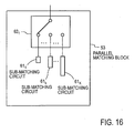
- Fig. 16 shows a third embodiment of the parallel matching block 53 using a switch.
- This parallel matching block 53 is constructed of K sub-matching circuits 61 1 to 61 K and an SPnT switch 62 1 which selectively connects any one of them.
- the respective sub-matching circuits 61 1 to 61 K have different reactances and the parallel matching block 53 can obtain approximately K reactance values by connecting the switch 62 1 to each sub-matching circuit.
- the sub-matching circuit can be constructed arbitrarily using a transmission line, lumped elements, etc. For example, using a variable reactance or an element having a variable capacitance function as the lumped element can realize finer reactance control.
- the embodiments of the matching circuit 50 shown in Figs. 4, 9, 10, 12 show the case where the parallel matching blocks 53 2 to 53 N are connected to one end of the series matching blocks 52 2 to 52 N through the switches 54 2 to 54 N .
- the characteristic of the switch 54 requires that the insertion loss at the frequency f 2 be small especially in an ON state and the isolation at the frequency f 1 be high in an OFF state.
- the insertion loss and isolation of the switch generally deteriorate as the operating frequency becomes higher. Therefore, when it is not possible to secure a sufficiently low insertion loss at the frequency f 2 and sufficient isolation at the frequency f 1 in the above described matching circuit 50, the characteristic of the matching circuit 50 may deteriorate.
- An embodiment of the matching circuit which solves this problem will be explained below.
- Fig. 17 shows a fifth embodiment of the matching circuit of the present invention.
- a case where the impedance of a signal source 23 has a frequency characteristic is shown.
- This embodiment corresponds to the embodiment in Fig. 9 with only the positions of the switch 54 2 and parallel matching block 53 2 connected in series switched round and the rest of the structure is the same as that in Fig. 9.
- the main matching block 51 is a matching circuit for an input signal of a frequency f 1 and is designed so that the impedance Z s (f 1 ) of the signal source 23 at a point B matches the load impedance Z L .
- the series matching block 52 2 is made up of a circuit element such as a transmission line so as not to influence signal transmission at the frequency f 1 between points A and B.
- the series matching block 52 2 may be made up of a transmission line whose characteristic impedance is equal to the output load impedance Z L or made up of a transmission line whose characteristic impedance is a certain Z T and converted to an output load impedance Z L by an impedance converter with no frequency characteristic at a port P 2 .
- the series matching block 52 2 and parallel matching block 53 2 together with the main matching block 51 arranged as described above are designed so that the signal source impedance Z s (f 2 ) matches the load impedance Z L at the port P 2 .
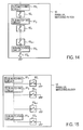
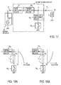
- the switch 54 2 is designed to be either in an ON or OFF state. More specifically, for example, the series matching block 52 2 is made up of a transmission line whose characteristic impedance matches the load impedance Z L at a frequency f 1 and the parallel matching block 53 2 is made up of a transmission line having a line length of ⁇ 1 /4, where ⁇ 1 is the wavelength of the signal of the frequency f 1 .
- the main matching block 51 is designed so as to establish matching between the signal source impedance Z s (f 2 ) and the load impedance Z L at the frequency f 2 with the switch 54 2 set to OFF. Therefore, when the switch 54 2 is OFF as shown in Fig. 18A, the voltage distribution along the parallel matching block 53 2 having a line length ⁇ 1 /4 with respect to the signal of the frequency f 1 becomes a maximum on the open end side, 0 at a connection point A, that is, short-circuited at the connection point A.
- the matching circuit 50 does not supply the signal of the frequency f 1 to the load circuit 28, establishes matching between the impedance of the signal source 23 and the impedance of the load circuit 28 for only the signal of the frequency f 2 and can supply the signal to the load circuit 28.
- the switch 54 2 is set to ON.
- the parallel matching block 53 2 having a line length ⁇ 1 /4 on the ground side is short-circuited, and therefore the voltage distribution for the signal of frequency f 1 becomes a maximum at the connection point A. That is, the parallel matching block 53 2 ideally has infinite impedance for the signal of frequency f 1 at the connection point A. Therefore, it is possible to eliminate the influence of the parallel matching block 53 2 at the frequency f 1 .
- the characteristic of the switch 54 2 requires high isolation at the frequency f 2 and a low insertion loss at the frequency f 1 .
- the parallel matching block 53 2 is connected to the connection point A, and therefore as described above, the parallel matching block 53 2 viewed from the connection point A by setting the switch 54 2 to ON/OFF can become short-circuited (impedance 0) or open (infinite impedance) for the signal of frequency f 1 . Therefore, even if the switch 54 2 itself does not have the required insertion loss or isolation characteristic, the influence is small.
- the input impedance of the parallel matching block 53 2 at the frequency f 1 at the connection point A also ideally becomes infinite, that is, left open and has no influence on the signal of the frequency f 1 .
- the characteristic required for the switch 54 2 is equivalent to that in Fig. 9.
- the mounting position of the switch 54 2 can be separated from the signal path (main matching block and series matching block), and therefore it has an advantage that mounting is easy.
- Fig. 19 shows a sixth embodiment of the matching circuit of the present invention.
- This embodiment is a modified embodiment of the embodiment in Fig. 17 and the switch 54 2 in the embodiment in Fig. 17 is connected to another parallel matching block 55 2 instead of a ground.
- the rest of the structure is the same as that in Fig. 17.
- the switch 54 2 need not satisfy a high-level requirement in the aspects of isolation and insertion loss, but when, for example, the design of each matching block which realizes matching at one frequency f 1 is determined, the degree of freedom of selecting another frequency f 2 at which matching can be achieved is not so large.
- the embodiment in Fig. 19 improves this aspect.
- This embodiment as well as that in Fig. 17 is a circuit for matching a signal source 23 of impedance Z s (f) connected to a port P 1 to the impedance viewed from the port P 2 .
- the embodiment in Fig. 17 operates, for example, as the matching circuit for signals of two frequency bands b 1 , b 2 shown in Fig. 5.
- the main matching block 51 is a matching circuit for an input signal of the frequency f 1 and designed so that the signal source impedance Z s (f 1 ) matches the load impedance Z L at the connection point B.
- the series matching block 52 2 is constructed of a circuit element such as a transmission line so as not to influence signal transmission of the frequency f 1 between the connection points B and A.
- the series matching block 52 2 may be made up of a transmission line whose characteristic impedance is equal to the load impedance Z L or may also be made up of a transmission path whose characteristic impedance is equal to a certain impedance Z T and Z T may also be converted to a load impedance Z L by an impedance converter with no frequency characteristic at the port P 2 .
- the design methods may vary depending on which of the insertion loss of the switch 54 2 at the frequency f 2 or the isolation characteristic becomes a greater problem.
- the design will be conducted as follows. With the switch 54 2 set to OFF, a matching circuit for the frequency f 2 is designed using the main matching block 51, series matching block 52 2 and parallel matching block 53 2 .
- the parallel matching block 53 2 as a solution of the design can have an arbitrary reactance component, and therefore the addition of the parallel matching block 53 2 to the signal path causes a loss to the signal of the frequency f 1 in many cases. Therefore, for the signal of frequency f 1 , the switch 54 2 is set to ON and another parallel matching block 55 2 is added to the parallel matching block 53 2 .
- the parallel matching block 55 2 is designed so that the impedance of the parallel matching blocks 53 2 , 55 2 at the frequency f 1 seen looking into the parallel matching block 53 2 from the connection point A in Fig. 19 becomes a maximum when the switch 54 2 is ON. This minimizes the influence of the parallel matching blocks 53 2 , 55 2 on the signal of the frequency f 1 when the switch 54 2 is ON.
- the switch 54 2 is set to ON and a matching circuit for the frequency f 2 is designed using the main matching block 51, series matching block 52 2 and parallel matching blocks 53 2 , 55 2 .
- the series circuit of the parallel matching blocks 53 2 and 55 2 as a solution of the design can have an arbitrary reactance component, and therefore the addition of the parallel matching blocks 53 2 , 55 2 to the signal path causes damage to the signal of the frequency f 1 in many cases. Therefore, when the circuit is used at the frequency f 1 , the switch 54 2 is set to OFF and the parallel matching block 55 2 is separated from the signal path.
- the parallel matching block 53 2 is designed so that the impedance at the frequency f 1 seen looking into the parallel matching block 53 2 from the connection point A in Fig. 19 becomes maximum. This minimizes the influence of the parallel matching blocks 53 2 , 55 2 on the signal of the frequency f 1 .
- the embodiment in Fig. 19 designs matching for a desired frequency using the two parallel matching blocks 53 2 , 55 2 , and therefore the degree of freedom of selecting a frequency is high and by selecting an optimal position of the switch 54 2 between the two parallel matching blocks 53 2 , 55 2 , it is possible to improve deteriorations of the matching circuit 50 by an insertion loss of the switch 54 2 as well as isolation.
- the insertion loss is caused by a resistance component included in the switch, but with regard to the position of the switch 54 2 , it is possible to reduce a loss in the circuit caused by the insertion of the switch by regarding the two parallel matching blocks 53 2 , 55 2 as one transmission line, determining the lengths of the two lines so as to be inserted into a place where the current distribution of the signal becomes a minimum at a certain position on the line.
- Fig. 20 shows a seventh embodiment of the matching circuit of the present invention, which is a modified example of the embodiments in Fig. 17 and Fig. 19.
- This embodiment differs from the embodiment in Fig. 19 in that the parallel matching blocks 53 2 , 55 2 are directly connected to each other and a switch 54 2 is inserted between the connection point thereof and a ground and the rest of the structure is the same as that in Fig. 19.
- Fig. 20 as well as Fig. 17 also shows a circuit for matching the impedance seen looking into the load from the port P 2 to the signal source 23 connected to the port P 1 , and the circuit operates as a matching circuit for two frequency bands b 1 , b 2 as in the case of Fig. 19.
- the main matching block 51 in Fig. 20 is a matching circuit for an input signal of the frequency f 1 as in the case of Fig. 19 and the design criteria thereof are the same, and therefore explanations thereof will be omitted.
- the switch 54 2 is set to OFF first and a matching circuit for the frequency f 2 is designed using the main matching block 51, series matching block 52 2 and parallel matching blocks 53 2 , 55 2 . Since the series circuit of the parallel matching blocks 53 2 , 55 2 as a solution of the design can have an arbitrary reactance component, and therefore the addition of this series circuit to the signal path influences the signal of the frequency f 1 in many cases. Therefore, in this embodiment, the switch 54 2 is set to ON when used at the frequency f 1 .
- the parallel matching block 53 2 is designed so that the impedance at the frequency f 1 seen looking into the parallel matching block 53 2 from the connection point A in Fig. 20 becomes a maximum when the switch 54 2 is set to ON.
- the switch 54 2 when the switch 54 2 is ON, it is possible to minimize the influence of the parallel matching blocks 53 2 , 55 2 on the impedance at the frequency f 1 .
- the parallel matching block 55 2 can be designed at an arbitrary reactance, and therefore it is possible to design a matching circuit for the frequency f 2 .
- Fig. 21 shows a seventh embodiment of the matching circuit of the present invention, which is a modified example of the embodiment in Fig. 19.
- Fig. 21 shows a case where the parallel matching block 53 2 in the matching circuit 50 shown in embodiment in Fig. 19 (where the isolation characteristic becomes a problem) is constructed of a series circuit of a switch 62 1 and a transmission line 61 1 as in the case of the embodiment in Fig. 9.
- the insertion loss and isolation of the switch 62 1 have frequency characteristics and both insertion loss and isolation generally deteriorate as the frequency increases.
- the parallel matching block 53 2 When operating the circuit at a frequency f 1 , if the switch 62 1 in the parallel matching block 53 2 is OFF and if the isolation of the switch 62 1 in the parallel matching block 53 2 cannot be sufficiently secured at the frequency f 1 , the parallel matching block 53 2 influences signal transmission of the frequency f 1 and produces a loss.
- the switch 54 2 which follows the parallel matching block 53 2 is set to ON.
- the parallel matching block 55 2 is designed so that the impedance seen looking into the parallel matching block 53 2 from the connection point A together with the parallel matching block 53 2 becomes a maximum. Therefore, when the structure in this embodiment is used, it is possible to minimize the influence of the parallel matching block 53 2 on the signal of the frequency f 1 even if the isolation of the switch 62 1 is insufficient at the frequency f 1 .
- the example of the structure of the parallel matching block 53 2 in Fig. 21 is also applicable to the embodiments shown in Fig. 17 and Fig. 20 and similar effects can be obtained in the respective matching circuits.
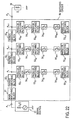
- Fig. 22 shows an eighth embodiment of the matching circuit of the present invention.
- This matching circuit is provided with a main matching block 51 and N-1 series matching blocks 52 2 to 52 N (2 ⁇ n ⁇ N) cascaded thereto and an output side connection point A n-1 of each series matching block 52 n is connected to a series circuit consisting of N parallel matching blocks 53 n1 to 53 nN through switches 54 n1 to 54 nN-1 .
- the circuit in Fig. 22 operates as a matching circuit for signals of N frequency bands.
- the main matching block 51 is a matching circuit for an input signal of a frequency f 1 .
- the N-1 series matching blocks 52 2 to 52 N connected in series are made up of circuit elements such as transmission lines so as not to influence signals of frequencies f 1 to f N .
- the N-1 series matching blocks 52 2 to 52 N may be constructed of transmission lines whose characteristic impedance is equal to the load impedance Z L or constructed of a transmission path whose characteristic impedance is equal to an impedance Z T and converted to a load impedance Z L at a port P 2 by an impedance converter with no frequency characteristic.
- the parallel matching blocks 53 n1 to 53 nN are designed so that the input impedance seen looking into the parallel matching block 53 n1 from the connection point A n-1 becomes a maximum at a frequency f m (m ⁇ n) by controlling switches 54 n1 to 54 nN-1 , and that the parallel matching blocks 53 n1 to 53 nN together with the main matching block 51 and series matching blocks 52 2 to 52 N form a matching circuit at a connection point A n-1 at a frequency f n (2 ⁇ n ⁇ N) when the switches 54 n1 to 54 nN-1 are set in different states.
- the switches 54 n1 to 54 nn-1 are set to ON and at least switch 54 nn of the switches 54 nn to 54 nN-1 is set to OFF and the parallel matching blocks 53 n1 to 53 nn are designed to be matched to the frequency f n .
- the switches 54 n1 to 54 np-1 (2 ⁇ p ⁇ N-1, p ⁇ n) are set to ON and at least the switch 54 np of the switches 54 np to 54 nN-1 is set to OFF, the parallel matching blocks 53 n1 to 53 np are added to the signal path at the connection point A n-1 so as to maximize the input impedance of the circuit made up of the parallel matching blocks 53 n1 to 53 nN with respect to the frequency f m at the connection point A n-1 .
- each series matching block and parallel matching block By constructing each series matching block and parallel matching block in this way, it is possible to realize a matching circuit for N frequency bands.
- N-1) series matching blocks 52 2 to 52 N N(N-1) parallel matching blocks 53 21 to 53 NN , N(N-1) switches 54 21 to 54 NN is shown, but it is also possible to realize the matching circuit using fewer switches and matching blocks than these blocks and switches depending on the characteristic of the signal source impedance Z s (f).
- switches 54 n1 to 54 nq-1 (1 ⁇ q ⁇ N) are set to ON and switch 54 nq is set to OFF, in addition to the parallel matching blocks 53 n1 to 53 nq connected to the connection point A n-1 , switches 54 k1 to 54 kr-1 (k>n, 1 ⁇ r ⁇ N) are set to ON and the switch 54 kr is set to OFF so that matching can be established for a frequency f s at a connection point A k-1 using some of the parallel matching blocks 53 k1 to 53 kr connected to the connection point A k-1 , the main matching block 51 and the series matching blocks 52 2 to 52 k .
- each of the cascade connections of the parallel matching blocks connected at each point other than the connection points A n-1 and A k-1 through switch control is designed so that the input impedance of each parallel matching block at the frequency f s seen looking into the corresponding parallel matching block from the connection point connected thereto becomes a maximum. This can minimize the influence of these parallel matching blocks on signal transmission of the frequency f s .
- the parallel matching blocks connected to points other than the connection points A n-1 and A k-1 can also be used as part of the matching circuit of the frequency f s through switch control.
- the number of series matching blocks becomes smaller than N-1 and it is thereby possible to reduce the number of parallel matching blocks and switches together with the decrease in the number of series matching blocks. Furthermore, it is possible to use a condition under which the input impedance is maximized, for example, when some of frequencies f 1 to f N have a relationship in which one frequency is an odd-number multiple of another, and therefore it is possible to reduce the number of switches.
- the parallel matching blocks so as to resonate at a plurality of frequencies out of the frequencies f 1 to f N , it is also possible to likewise use a condition under which the input impedance can be maximized and thereby reduce the number of switches and parallel matching blocks.
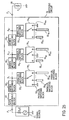
- Fig. 23 shows a ninth embodiment of the matching circuit of the present invention.
- This embodiment corresponds to the embodiment in Fig. 22 with the switches removed from the cascade connection of N parallel matching blocks connected to the connection points A n-1 and N-1 switches connected alternately, with N parallel matching blocks 53 n1 to 53 nN cascaded and with connection points between the respective parallel matching blocks and the terminal of the final stage parallel matching block 53 nN connected opposite to the connection point A n-1 grounded via switches 54 n1 to 54 nN .
- the circuit in Fig. 23 operates as a matching circuit for signals of N frequency bands, for example.
- the main matching block 51 is a matching circuit for an input signal of a frequency f 1 .
- Series matching blocks 52 2 to 52 N are constructed in the same way as for the embodiment in Fig. 22.
- the switches 54 n1 to 54 nN are set to OFF and the respective parallel matching blocks 53 n1 to 53 nN , are designed for the frequencies f 1 to f N so as to construct a matching circuit for the frequency f n with the main matching block 51, series matching blocks 52 2 to 52 n-1 and parallel matching blocks 53 n1 to 53 nN .
- the parallel matching blocks 53 n1 to 53 nN through such switch control at a frequency f m (1 ⁇ m ⁇ N, m ⁇ n), for example, as setting a switch 54 np (1 ⁇ p ⁇ N) to ON, the influence of the parallel matching blocks 53 n1 to 53 np on signal transmission of a frequency f m can be minimized by designing the cascade connection of the parallel matching blocks 53 n1 to 53 np so that the impedance at the frequency f m seen looking into the parallel matching block 53 n1 from the connection point A n-1 in Fig. 23 becomes a maximum.
- the switch 54 np (1 ⁇ p ⁇ N) is set to ON for a frequency f n , for example, and the respective matching blocks are designed for the frequencies f 1 to f N so as to construct a matching circuit for the frequency f n using the main matching block 51, series matching blocks 52 2 to 52 n , parallel matching blocks 53 n1 to 53 np .
- the parallel matching blocks 53 n1 to 53 nN through such switch control at the frequency f m (1 ⁇ m ⁇ N, m ⁇ n), for example, as setting a switch 54 nq (1 ⁇ q ⁇ N, p ⁇ q) to ON, the influence of the parallel matching blocks 53 n1 to 53 nN on signal transmission of the frequency f m can be minimized by designing the cascade connection of the parallel matching blocks 53 n1 to 53 nq so that the impedance at the frequency f m seen looking into the parallel matching block 53 n1 is from the connection point A n-1 in Fig. 23 becomes a maximum.
- the circuit may be realized with fewer switches or matching blocks than these switches and blocks.
- the parallel matching blocks 53 n1 to 53 nr+1 (r ⁇ N) connected to the connection point A n-1 for matching at the frequency f n the parallel matching blocks 53 k1 to 53 ks+1 (s ⁇ N) connected to the connection point A k-1 are used together. Constructing the matching circuit with a combination of parallel matching blocks connected to a plurality of connection points A x in this way causes the number of series matching blocks to become smaller than N-1 and can also reduce the number of parallel matching blocks and switches together with the decrease in the number of the series matching blocks.
- the parallel matching blocks 53 n1 to 53 nN and 53 k1 to 53 kN through such switch control at the frequency f m (1 ⁇ m ⁇ N, m ⁇ n), for example, as setting switches 54 nR (1 ⁇ R ⁇ N) and 54 nS (1 ⁇ S ⁇ N) to ON, the influence of the parallel matching blocks 53 n1 to 53 nr and 53 k1 to 53 ks on signal transmission of the frequency f m can be minimized by designing the cascade connection of the parallel matching blocks 53 n1 to 53 nR and 53 r1 to 53 rs so that the impedance at the frequency f m seen looking into the parallel matching blocks 53 n1 and 53 r1 from the connection points A n-1 and A r-1 becomes a maximum.
- Fig. 24 shows a tenth embodiment of the matching circuit of the present invention.
- the embodiment in Fig. 24 has a structure corresponding to the embodiment shown in Fig. 23 with a switch 54 np inserted between the parallel matching blocks 53 np and 53 np+1 .
- This embodiment obtains effects similar to those of the embodiment shown in Fig. 19 and Fig. 22.
- Fig. 25 shows an eleventh embodiment of the matching circuit of the present invention.
- parallel matching blocks 53 2 to 53 N are connected to output side connection points A 1 to A N-1 of (N-1) series matching blocks 52 2 to 52 N cascaded to a main matching block 51 and an SpNT switch 54 n is connected to each parallel matching block 53 n .
- N parallel matching blocks 55 n1 to 55 nN are connected to N output terminals of the respective switches 54 n .
- a parallel matching block 55 nn directly grounds the nth terminal of the switch 54 n , but it may also be left open.
- the circuit in Fig. 25 also operates as a matching circuit 50 for signals of N frequency bands.
- the main matching block 51 in Fig. 25 is a matching circuit for an input signal of a frequency f 1 .
- the parallel matching block 55 nn is grounded or left open.
- the switch 54 n is connected to the parallel matching block 55 nm .
- the parallel matching block 55 nm is designed so that the impedance at the frequency f m seen looking into the parallel matching block 53 n from the connection point A n-1 becomes a maximum. This minimizes the influence of the parallel matching block 53 n on signal transmission of the frequency f m .
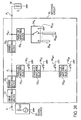
- Fig. 26 shows a twelfth embodiment of the matching circuit of the present invention.
- the embodiment in Fig. 26 has a structure combining the embodiment in Fig. 23 with the embodiment in Fig. 25.
- Figs. 22 to Fig. 25 it is also possible to arbitrarily combine Figs. 22 to Fig. 25. The operation is similar to that explained in each of the foregoing embodiments.
- the structure of the main matching block 51 in the embodiments in Fig. 17 and Figs. 19 to 26 can be selected arbitrarily.
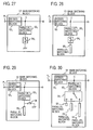
- a first embodiment of the main matching block 51 is shown in Fig. 27.
- the main matching block 51 is constructed of a series matching block 52 1 connected to a port P 1 , a parallel matching block 53 1 , one end of which is connected to the output side of the series matching block 52 1 and a switch 54 1 inserted between the other end of the parallel matching block 53 1 and ground.
- the series matching block 52 1 is constructed of a circuit element such as a transmission line so as not to influence signal transmission of a frequency f n (n ⁇ N) between points B-A in Fig. 17, for example.
- a circuit element such as a transmission line so as not to influence signal transmission of a frequency f n (n ⁇ N) between points B-A in Fig. 17, for example.
- it may be constructed of a transmission line whose characteristic impedance is equal to an output load impedance Z L or may be constructed of a transmission line whose characteristic impedance is equal to a certain impedance Z T and converted to a load impedance Z L at a port P 2 by an impedance converter with no frequency characteristic.
- the series matching block 52 1 and parallel matching block 53 1 are designed so as to match the impedance Z L at the port P 2 in Fig. 17.
- the design is made with the switch 54 1 in a state of either ON or OFF.
- the matching circuit of a frequency f 1 is designed assuming that the state of the switch 54 1 is OFF.
- the parallel matching block 53 1 becomes an open-end line having a line length ⁇ m /4 ( ⁇ m : wavelength at frequency f m , 2 ⁇ m ⁇ N)
- the signal of the frequency f m is short-circuited at a connection point C and cannot be used at the frequency f m .
- the switch 54 1 needs only to be set to ON when used at the frequency f m and at this time, the input impedance at the connection point C of the parallel matching block 53 1 at the frequency f m is ideally infinite, that is, it is possible to eliminate the influence of the parallel matching block 53 1 at the frequency f m . Furthermore, the switch 54 1 is set to ON, the matching circuit at the frequency f 1 is designed and when the parallel matching block 53 1 becomes a circuit equivalent to a short-circuited line having a line length ⁇ m /2, the circuit is short-circuited at the connection point C at the frequency f m .
- the input impedance of the parallel matching block 53 1 at the connection point C is likewise ideally infinite, that is, left open and has no influence on the signal of the frequency f m .
- Fig. 28 shows a second embodiment of the main matching block 51 in the embodiments of the present invention in Fig. 17 and Figs. 19 to 26.
- a parallel matching block 53 1 is connected to an end of a series matching block 52 1 and a parallel matching block 55 1 is connected to the parallel matching block 53 1 through a switch 54 1 .
- the series matching block 52 1 of the main matching block 51 is constructed of a circuit element such as a transmission line so as not to influence signal transmission of a frequency f n (n ⁇ N) between points B-A in Fig. 17, for example.
- the design method varies depending on which characteristic of insertion loss of the switch 54 1 at the frequency f 2 and isolation characteristic has a greater problem.
- the switch 54 1 is set to OFF and a matching circuit is designed for a frequency f 1 using the series matching block 52 1 and parallel matching block 53 1 .
- the parallel matching block 53 1 as a solution of the design can have an arbitrary reactance component, and so the addition of the parallel matching block 53 1 to the signal path at the connection point C causes a loss to the signal of a frequency f m (2 ⁇ m ⁇ N) in many cases. Therefore, when used at the frequency f m , the switch 54 1 is set to ON and the parallel matching block 55 1 is added to the signal path.
- the parallel matching block 55 1 is designed so that when the switch 54 1 is ON, the impedance at the frequency f m seen looking into the parallel matching block from the connection point C becomes a maximum. When the switch 54 1 is ON, this minimizes the influence of the parallel matching blocks 53 1 , 55 1 on the signal of the frequency f m .
- the switch 54 1 is set to ON, a matching circuit for the frequency f 1 is designed using the series matching block 52 1 and parallel matching blocks 53 1 , 55 1 .
- the series circuit of the parallel matching blocks 53 1 , 55 1 as a solution of the design can have an arbitrary reactance component, and so the addition of the parallel matching blocks 53 1 , 55 1 to the signal path causes a loss to the signal of the frequency f m in many cases. Therefore, when used at the frequency f m , the switch 54 1 is set to OFF and the parallel matching block 53 1 is separated from the signal path.
- the parallel matching block 53 1 is designed so that the impedance at the frequency f m seen looking into the parallel matching block from the connection point C becomes a maximum. This can minimize the influence of the parallel matching blocks 53 1 , 55 1 on the signal of the frequency f m .
- Fig. 29 shows a third embodiment of the main matching block 51 in the embodiments in Fig. 17, Figs. 19 to 26 according to the present invention.
- This example has a structure in which the parallel matching blocks 53 1 and 55 1 in the embodiment in Fig. 28 are directly connected to each other, and between the connection point thereof and ground a switch 54 1 is inserted.
- the series matching block 52 1 of the main matching block 51 is constructed of a circuit element such as a transmission line so as not to influence signal transmission of a frequency f n (n ⁇ N) between points B-A in Fig. 17, for example.
- the switch 54 1 is set to OFF and a matching circuit for the frequency f 1 is designed using the series matching block 52 1 , parallel matching blocks 53 1 , 55 1 .
- the series circuit of the parallel matching blocks 53 1 , 55 1 as a solution of the design can have an arbitrary reactance component, and so the addition of this series circuit to the signal path influences the signal of the frequency f m (2 ⁇ m ⁇ N) in many cases. Therefore, in this embodiment, when used at the frequency f m , the switch 54 1 is set to ON.
- the parallel matching block 53 1 is designed so that the impedance at the frequency f m seen looking into the parallel matching block from the connection point C becomes a maximum when the switch 54 1 is ON. This can minimize the influence of the parallel matching blocks 53 1 , 55 1 on the impedance of the signal of the frequency f m when the switch 54 1 is ON.
- the parallel matching block 55 1 can be designed at an arbitrary reactance, and therefore it is possible to design a matching circuit for the frequency f 1 .
- Fig. 30 shows a fourth embodiment of the main matching block 51 in Fig. 17, Figs. 19 to 26 according to the present invention.
- This embodiment corresponds to the structure of the embodiment in Fig. 28 in which an SPNT switch is used as a switch 54 1 and parallel matching blocks 55 11 to 55 1N are connected to N output ends of the switch 54 1 .
- the series matching block 52 1 of the main matching block 51 is constructed of a circuit element such as a transmission line so as not to influence signal transmission of a frequency f n (n ⁇ N) between points B-A in Fig. 17, for example.
- the circuit is designed so as to construct a matching circuit for the frequency f 1 using the series matching block 52 1 , parallel matching blocks 53 1 , 55 11 .
- the switch 54 1 is connected to the parallel matching block 55 1m .
- the parallel matching block 55 1m is designed so that the impedance at the frequency f m seen looking into the parallel matching block 53 1 from the connection point C becomes a maximum. This can minimize the influence of the parallel matching blocks 53 1 , 55 1m on signal transmission of the frequency f m .
- main matching block 51 allows the switch mounting position to be separated from the signal path (main matching block or series matching block), which provides an advantage that mounting is easy.
- the structure of the main matching block 51 shown in Figs. 27 to 3 0 may also be applied to the main matching block 51 in the embodiments of the matching circuit shown in Figs. 4, 9, 10, 12, 13.
- an arbitrary parallel matching block may also be constructed as in the case of the parallel matching block 53 shown in Fig. 14.
- the parallel matching block 53 is provided with a variable reactance function and the overall matching circuit can perform matching for more frequencies. That is, by setting ON the switches in Fig. 14 one by one starting with the switch 62 1 and sequentially connecting the sub-matching circuits 61 1 to 61 K , the parallel matching block 53 can take approximately K reactance values.
- the parallel matching block 53 in Fig. 14 to one parallel matching block of the matching circuits in Figs. 17, 19, it is possible to further increase the number of frequencies that can be matched by approximately K.
- an arbitrary parallel matching block in the embodiments in Fig. 17, Figs. 19 to 26 may also be constructed in the same way as the parallel matching block 53 shown in Fig. 15.
- the switch 64 1 when the switch 64 1 is ON, one side of the switch 64 1 is grounded, and so the sub-matching circuits 63 2 to 63 k do not influence the reactance value of the parallel matching block 53 and the reactance of the parallel matching block 53 is determined by only the sub-matching circuit 63 1 .
- the switch 64 k when the switch 64 k is set to ON, the sub-matching circuits 63 k+1 to 63 K do not influence the reactance value of the parallel matching block 53 and the reactance of the parallel matching block 53 is determined by the sub-matching circuits 63 1 to 63 k . Therefore, by setting the switch 64 k to ON, the parallel matching block 53 can obtain approximately K reactance values.
- the parallel matching block 53 in Fig. 15 to an arbitrary parallel matching block 53 in the matching circuit 50 in Fig. 17, Figs. 19 to 26 it is possible to increase the number of frequencies that can be matched by approximately K.
- the sub-matching circuit may also be arbitrarily constructed using a transmission line, lumped element, etc.
- a transmission line lumped element, etc.
- an element having a variable reactance function or variable capacitance function as the lumped element it may be possible to perform finer reactance control.
- the structures of the main matching block, series matching block, parallel matching block and sub-matching circuit are not particularly limited if their structures at least satisfy the above described conditions.
- the matching circuit may be constructed using, for example, a lumped circuit or a distributed circuit or combining these circuits.
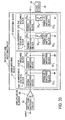
- Fig. 31 shows a first application example of the matching circuit of the present invention applied to an amplifier.
- the figure shows a case where this amplifier uses the matching circuit shown in Fig. 4 as an input side matching circuit 50 of an amplification element 26 and uses the matching circuit shown in Fig. 9 as an output side matching circuit 50' of the amplification element 26. Therefore, this amplifier amplifies the signals with two frequency bands whose center frequencies are f 1 , f 2 shown in Fig. 5.
- the switch 54 2 of both matching circuits 50, 50' are left open. This allows both the input side and output side to be matched at the frequency f 1 and to perform amplification satisfactorily.
- the switches 54 2 of both matching circuits 50, 50' are closed. This allows the input side matching circuit 50 and output side matching circuit 50' as a whole to establish matching at the frequency f 2 and thereby perform amplification satisfactorily.
- the amplification element 26 allows amplification of signals of two bands.
- any one of the matching circuits 50 shown in Fig. 10, Fig. 12, Fig. 13, Fig. 17, Figs. 19 to 26 can be used as the input side and output side matching circuits 50, 50' of the amplification element 26.
- Each matching block in Fig. 32 can be constructed using a lumped element made up of resistance, inductance, capacitance or a distributed element having a characteristic equivalent thereto.
- the application example in Fig. 32 is a design example of an amplifier used in 900 MHz/2 GHz bands.
- the main matching block 51 is a 2 GHz matching circuit
- the parallel matching block 53 2 is a block which changes the entire input side matching circuit 50 and the entire output side matching circuit 50' each to a 900 MHz matching circuit.
- Both switches 54 2 are kept open for a 2 GHz input signal.
- an input signal is transmitted through the series matching block 52 2 and 2 GHz main matching block 51 and input to an input terminal of a field effect transistor (FET) as the amplification element 26.
- FET field effect transistor
- the output side matching circuit 50' the signal is transmitted through the 2 GHz main matching block 51 and series matching block 52 2 and output to the port P 2 .
- the switches 54 2 of both the input side and output side matching circuits 50, 50' are closed and in the input side matching circuit 50, a parallel capacitor making up the parallel matching block 53 2 is inserted to construct a matching circuit of 900 MHz as a whole. Also in the output side matching circuit 50', a capacitor making up the parallel matching block 53 2 is inserted to construct a matching circuit of 900 MHz as a whole.
- the series matching block 52 2 can be constructed of a transmission line having a characteristic impedance equivalent to the amplifier input/output impedance or a circuit by lumped element equivalent thereto, etc. In this way, in this application example, it is possible to construct an amplifier which can be selectively matched for signals of two frequency bands by switching between ON/OFF of the switches 54 2 of the input side and output side matching circuits 50, 50'.
- amplification element 26 is not provided for each signal band individually. It is possible to construct a multi-band high-efficiency power amplifier by using only one wideband amplification element 26 to reduce the number of amplification elements and optimizing the output side matching circuit 50' which is a peripheral circuit of this wideband amplification element 26 for each signal band.
- this matching circuit of the present invention is used as the output side matching circuit 50' of an amplifier, a harmonics control block for controlling harmonics is used together in addition to the matching block from the standpoint of operating the power amplifier with high efficiency.
- the output side matching circuit 50' in Fig. 33 operates the amplification element 26 as a multi-band high efficiency amplifier for signals of two bands of the frequencies f 1 and f 2 shown in Fig. 5, for example.
- the aforementioned various matching circuits as the input side matching circuit 50, use one matching circuit of a design which can establish matching over the entire band of an estimated input signal or use a plurality of matching circuits used by being switched for each signal band.
- the output side matching circuit 50' in this applied embodiment is constructed of a first harmonics control block 51 A, a first matching block 51B, a second harmonics control block 57A and a second matching block 57B.
- the first harmonics control block 51A and first matching block 51B make up a main matching block 51 and the second harmonics control block 57A and second matching block 57B make up an additional block 57.
- the combination of the first matching block 51B and the second matching block 57B functions as the aforementioned matching circuit of the present invention and the combination of the first harmonics control block 51 A and the second harmonics control block 57A controls the harmonics components of the signals of fundamental frequencies f 1 , f 2 and the amplifier as a whole improves the efficiency of power amplification.
- the first harmonics control block 51A of the output side matching circuit 50' is a circuit which terminates harmonics of the frequency f 1 of the signal band b 1 in Fig. 5 and is made up of a series matching block 52 11 and a parallel matching block 53 11 . More specifically, it is a termination circuit with a double-wave frequency 2f 1 as shown in Fig.
- the voltage and current of the second order harmonic wave on the transmission line 52 11 are distributed as shown in Fig. 34A and short-circuited at the port P 1 .
- the length of the open-end line is designed so that the line is left open at the port P 1 .
- the parallel matching block 53 11 can be constructed using an end short-circuited line simply having a certain length or using a lumped element and the amount of delay is adjusted depending on the structure of the parallel matching block 53 11 .
- the first matching block 51B of the output side matching circuit 50' in Fig. 33 is a circuit which matches the amplification element 26 and the output load in the frequency band in the signal band b 1 and made up of a series matching block 52 12 and a parallel matching block 53 12 .
- a series matching block 52 12 made up of a transmission line
- the parallel matching block 53 12 made up of a transmission line.
- Fig. 35 is an example where an open-end line is used as the parallel matching block 53 12 .
- An end short-circuited line may also be used.
- a circuit using a combination of lumped elements can also be used for the parallel matching block 53 12 .
- the series matching block 52 12 can also be constructed as a delay circuit using a transmission line, etc., and the amount of delay is adjusted according to the structure of the parallel matching block 53 12 .
- the second harmonics control block 57A and second matching block 57B of the additional block 57 of the output side matching circuit 50' in Fig. 33 are circuits for terminating harmonics of the frequency f 2 of the signal band b 2 in Fig. 5 and matching the amplification element 2 to the output load in the signal band b 2 of the frequency f 2 .
- the second harmonics control block 57A corresponds to the first harmonics control block 51A in the main matching block 51 and is made up of a series matching block 52 21 , a switch 54 21 and a parallel matching block 53 21 .
- the second matching block 57B also corresponds to the first matching block 51B and is made up of a series matching block 52 22 , a switch 54 22 and a parallel matching block 53 22 .
- the structures of the respective matching blocks 52 12 , 52 22 , 53 12 , 53 22 are the same as those of the respective matching blocks in the above described first harmonics block 51A and the first matching block 51B and are designed using the frequency f 2 as
- the switches 54 21 and 54 22 of the additional block 57 are closed, an input signal is output after passing through the first harmonics control block 51A, first matching block 51B, and further second harmonics control block 57A and second matching block 57B.
- the harmonics to be controlled in the first harmonics control block 51A is sufficiently higher than the frequency f 2 , and therefore the second harmonics control block 57A and second matching block 57B of the additional block 57 can be easily designed without being influenced by the first harmonics control block 51A so much. Therefore, the matching circuit can be designed for the frequency f 2 without being influenced by the first harmonics control block 51A and the first matching block 51B.
- the output side matching circuit 50' in this case performs impedance matching in the signal band b 2 and harmonics controlling in the frequency f 2 .
- each harmonics control block and each matching block only need to be arranged in the order in which the characteristic is optimized and they are not limited to the order shown in Fig. 33.
- Fig. 36 it is possible to adopt a structure in which the positions of the first harmonics control block 51A and first matching block 51 B, and the positions of the second harmonics control block 57A and second matching block 57B are switched round.
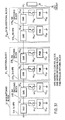
- FIG. 37 an embodiment which is an expansion of the embodiment in Fig. 33 will be explained.
- This corresponds to a circuit with (N-1) additional blocks 57 1 to 57 N-1 further added to the main matching block 51 made up of the first harmonics control block 51A and the first matching block 51B. That is, this embodiment corresponds to a matching circuit obtained by combining the second harmonics control block 57A and the second matching block 57B as a first additional block 57 1 and further cascading (N-2) (where, N ⁇ 3) additional blocks to this additional block.
- This (N-1)th additional block 57 N-1 consists of an Nth harmonics control block 57A N and an Nth matching block 57B N
- the (n-1)th additional block 57 n-1 is a circuit which terminates harmonics of a frequency f n in the signal band b n in Fig. 11 and matches the amplification element and the output load in the band of the frequency f n .
- the structure of each additional block is similar to the structure having the second harmonics control block 57A 2 and second matching block 57B 2 of the first additional block 57 1 and designed at the frequency f n as a fundamental wave.
- This expanded embodiment shows the case where the first harmonics control block 51A and first matching block 51B making up the main matching block 51 are also provided with switches 54 11 , 54 12 for switching ON/OFF, but these switches are not always necessary.
- Each series matching block does not influence signal transmission of f n and the series matching blocks 52 11 to 52 n1 and 52 12 to 52 n2 of the first to nth matching blocks 57B 1 to 57B n and the parallel matching block 53 22 of the nth matching block 57B n connected in parallel to the series matching blocks 52 11 to 52 n1 of the first to nth harmonics control blocks 57A 1 to 57A n can form a matching to an arbitrary impedance. Therefore, it is possible to design a matching circuit for the frequency f n without being influenced by each harmonics control block and each matching block which include open switches.
- harmonics control it is possible to perform harmonics control for the frequency f n without being influenced by each harmonics control block and each matching block which include open switches.
- This output matching circuit carries out impedance matching for the frequency f n and harmonics control of the frequency f n .
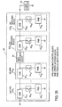
- Figs. 38 to 41 modified examples of the embodiment in Fig. 33 for improving the efficiency of the amplifier will be explained further.
- the embodiments in these figures are expansions of the embodiment in Fig. 33. That is, the insertion positions of the harmonics control block and matching block connected as additional blocks are not limited to the positions shown in Fig. 33, but arranged in the order allowing a better characteristic with the relationship with other harmonics control blocks and matching blocks taken into consideration.
- Fig. 38 shows an embodiment in which a main matching block 51, harmonics control blocks 57A 2 to 57A N and matching blocks 57B 2 to 57B N are arranged in that order, Fig.
- Fig. 39 shows an embodiment in which harmonics control blocks 57A 2 to 57A N , main matching block 51 and matching blocks 57B 2 to 57B N are arranged in that order
- Fig. 40 shows an embodiment in which matching blocks 57B 2 to 57B N , main matching block 51 and harmonics control blocks 57A 2 to 57A N are arranged in that order
- Fig. 41 shows an embodiment in which harmonics control blocks 57A 2 to 57A N , matching blocks 57B 2 to 57B N and main matching block 51 are arranged in that order.
- the switches 54 n1 , 54 n2 included in the nth harmonics control block 57A N and the nth matching block 57B N are ON/OFF, it is possible to match the entire output side matching circuit 50' in N frequency bands and construct a harmonics control circuit most suitable for improving the efficiency at each frequency.
- the number of SPST switches required for one combination of harmonics control block and matching block is as small as 2 and then, only 2(N-1) switches at most are required.
- the arrangement of the respective harmonics control blocks and respective matching blocks need only to follow the order in which the characteristic is optimized and is not limited to the order described above in Fig. 37.
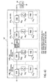
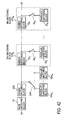
- Fig. 42 is an example where the parallel matching block 53 shown in Fig. 16 is applied to the group of the harmonics control blocks 57A 2 to 57A N shown in Fig. 38 and when, for example, the centrer frequency of an input signal is f n , the SPNT switch 54A is changed and connected to the nth parallel matching block.
- the nth parallel matching block is designed as a harmonics control circuit of a frequency f n .
- the nth parallel matching block connected in parallel to the first to nth series matching blocks can establish matching to an arbitrary impedance. Therefore, it is possible to design a matching circuit for f n without being influenced by the respective parallel matching blocks and the respective matching blocks including open switches.
- Each harmonics control block and each matching block can be constructed using resistance, inductance, capacitance or other lumped elements or distributed element having a characteristic equivalent thereto.
- the output side matching circuit 50' of the above described embodiment may also be applied to an input side matching circuit. Furthermore, the matching circuit of the above described embodiment establishes all impedance matching by adjusting amounts of delay of the parallel matching block and series matching block, but the amount of delay may be 0 depending on the circuit design. When the amount of delay of the series matching block of the additional block is 0, the corresponding switch is not necessary.
- the embodiments in Figs. 31, 32 have shown the example where the matching circuit 50 shown in Fig. 4 is applied as examples of the matching circuits 50, 50', but the matching circuit 50 shown in Figs. 17, 19, 20, 21 may also be used. Furthermore, the embodiments have shown the case where the series matching block 52 2 and the parallel matching block 53 2 connected thereto through the switch 54 2 shown in Fig. 4 or Fig. 9 are used as an example of each harmonics control block 57A and matching block 57B each including a switch in the embodiment in Fig. 36, but it is also possible to apply a combination of the series matching block 52 2 and the parallel matching block 53 2 and switch 54 2 connected thereto in the matching circuit 50 shown in Fig. 17 or a combination of the series matching block 52 2 and the parallel matching blocks 53 2 , 55 2 and switch 54 2 connected thereto in the matching circuit 50 shown in Figs. 19, 20, 21.
- frequency bands include a fourth-generation mobile communication system (5 GHz band, etc.), third-generation mobile communication system (2 GHz band) and other systems (800 MHz band, 1.5 GHz band for PDC, 2.4 GHz for GSM, PHS, wireless LAN, etc.) but the frequency bands are not limited to these systems.
- 5 GHz band, etc. fourth-generation mobile communication system
- 2 GHz band third-generation mobile communication system
- other systems 800 MHz band, 1.5 GHz band for PDC, 2.4 GHz for GSM, PHS, wireless LAN, etc.
- the present invention eliminates the necessity for constructing separate matching circuits for different signal frequency bands of input signals and can thereby reduce the number of parts as well as the mounting area. It also minimizes the number of changeover switches to thereby reduce resulting losses and reduce the size of the overall shape and structure.
- the matching circuit of the present invention it is not necessary to construct as many combinations of amplification elements, harmonics control circuits and matching circuits as frequency bands of an input signal and it is thereby possible to reduce the number of parts and reduce the mounting area. Furthermore, especially when the matching circuit is changed, it is possible to reduce the number of switches used, also use SPST switches in a simple structure and therefore drastically reduce insertion losses caused by switches. Therefore, the present invention is suitably applicable to construction of a small multi-band high-efficiency power amplifier.
- the matching circuit of the present invention even in a cell environment in which frequency bands used for a plurality of mobile communication services are mixed, changing this switch causes the reactance of the circuit to change and make the entire matching circuit applicable to multi-bands. Furthermore, according to the matching circuit of the present invention, it is possible to provide a multi-band matching circuit which allows impedance matching to be established even when a switch having insufficient insertion loss and isolation characteristic is used.
Landscapes
- Engineering & Computer Science (AREA)
- Computer Networks & Wireless Communication (AREA)
- Signal Processing (AREA)
- Power Engineering (AREA)
- Microwave Amplifiers (AREA)
- Amplifiers (AREA)
- Transmitters (AREA)
Abstract
Description
Claims (19)
- A matching circuit comprising:a main matching block inserted in a signal path, with matching established in at least a first frequency band;a series matching block inserted in said signal path, one end of which is connected to said main matching block, with matching to said main matching block established in said first frequency band; anda series connection between a parallel matching block and a switch, in whichone end of said series connection is connected to said signal path at the other end of said series matching block and setting said switch to ON/OFF realizes selective matching in said first frequency band and a second frequency band which is different from said first frequency band.
- A matching circuit according to Claim 1,
in which one end of said series connection is one end of said switch and connected to said signal path. - A matching circuit according to Claim 1,
in which one end of said series connection is one end of said parallel matching block and connected to said signal path. - A matching circuit according to Claim 3, further comprising a second parallel matching block connected to said switch at the other end of said series connection.
- A matching circuit according to Claim 3, further comprising a second parallel matching block connected to a connection point between said parallel matching block and said switch.
- A matching circuit according to any one of Claim 1, 2 or 3,
in which said main matching block comprises a second series matching block inserted in said signal path and a second series connection in which a second switch and a second parallel matching block are connected in series, and
one end of said second series connection is connected to one end of said second series matching block. - A matching circuit according to Claim 6,
in which said one end of said second series connection is one end of said second parallel matching block, connected to one end of said second series matching block, and
said switch is grounded at the other end of said second series connection. - A matching circuit according to Claim 7, further comprising a third parallel matching block, one end of which is connected to a connection point between said second parallel matching block and said second switch.
- A matching circuit according to Claim 6,
in which said one end of said second series connection is one end of said second parallel matching block, connected to one end of said second series matching block and provided with a third parallel matching block connected to the other end of said second series connection. - A matching circuit according to any one of Claim 1, 2 or 3,
in which said parallel matching block comprises a plurality of sub-matching circuits and one or more second switches alternately connected in series to said plurality of sub-matching circuits. - A matching circuit according to any one of Claim 1, 2 or 3,
in which said parallel matching block comprises a plurality of sub-matching circuits connected in series and a second switch inserted between the respective connection points between said plurality of sub-matching circuits and ground. - A matching circuit according to any one of Claim 1, 2 or 3, further comprising one or more second series matching blocks connected in series to said series matching block,
in which a second series connection of a second parallel matching block and a second switch is connected at one end of said second series matching block. - A matching circuit according to any one of claim 1, 2 or 3,
in which said switch is a single pole N throw switch which has a single pole and N terminals, said single pole being connected to said signal path,
said parallel matching blockand at least one second parallel matching block are connected to said N terminals respectively, and
said switch can select any one of said parallel matching block and said second parallel matching block connected to said N terminals and connect the selected block to said signal path. - A matching circuit according to any one of Claim 1, 2 or 3, further comprising:a second series matching block inserted in said signal path;a second parallel matching block connected between one end of said second series matching block and ground;a first harmonics control block which eliminates a harmonic component of a signal of a first frequency in said signal path using said blocks;a third series matching block inserted in said signal path;a series connection of a third parallel matching block connected between one end of said third series matching block and ground, and a second switch; anda second harmonics control block which controls a harmonics component of a signal of a second frequency different from said first frequency.
- A matching circuit according to Claim 14,
in which said main matching block comprises a fourth series matching block inserted in said signal path and a fourth parallel matching block connected between one end of said fourth series matching block and ground. - A matching circuit according to Claim 15, further comprising:a third switch provided in series to said second parallel matching block in said first harmonics control block; anda fourth switch provided in series to said fourth parallel matching block in said main matching block.
- A matching circuit according to Claim 14,
in which said main matching block constitutes a first matching block,
a combination of said first series matching block and said first series connection constitutes a second matching block,
a combination of said second matching block and said second harmonics control block constitutes an additional block, and
at least one second additional block similar to said additional block is inserted in said signal path. - A matching circuit comprising:in which said first and second single pole N throw switches select any one of said directly connected transmission line and (N-1) matching blocks, connect the selected one to said main matching block, and can thereby realize selective matching in said first frequency band and any one of at least (N-1) frequency bands different from said first frequency band.first and second single pole N throw switches, N being an integer of 2 or greater;a main matching block connected to the single pole side of said second single pole N throw switch, with matching established in a first frequency band; anda transmission line and (N-1) matching blocks connected between N terminals of said first and second single pole N throw switches,
- A power amplifier comprising said matching circuit according to any one of Claims 1 to 18 as at least one of an input side matching circuit and an output matching circuit of an amplification element.
Applications Claiming Priority (7)
| Application Number | Priority Date | Filing Date | Title |
|---|---|---|---|
| JP2003069906 | 2003-03-14 | ||
| JP2003069906 | 2003-03-14 | ||
| JP2003206615 | 2003-08-07 | ||
| JP2003206615 | 2003-08-07 | ||
| JP2004013251 | 2004-01-21 | ||
| JP2004013251 | 2004-01-21 | ||
| PCT/JP2004/003407 WO2004082138A1 (en) | 2003-03-14 | 2004-03-15 | Matching circuit |
Publications (2)
| Publication Number | Publication Date |
|---|---|
| EP1605589A1 true EP1605589A1 (en) | 2005-12-14 |
| EP1605589A4 EP1605589A4 (en) | 2007-03-21 |
Family
ID=32995603
Family Applications (1)
| Application Number | Title | Priority Date | Filing Date |
|---|---|---|---|
| EP04720743A Withdrawn EP1605589A4 (en) | 2003-03-14 | 2004-03-15 | ADAPTATION CIRCUIT |
Country Status (5)
| Country | Link |
|---|---|
| US (1) | US8098114B2 (en) |
| EP (1) | EP1605589A4 (en) |
| JP (1) | JP4464919B2 (en) |
| CN (1) | CN1762097B (en) |
| WO (1) | WO2004082138A1 (en) |
Cited By (13)
| Publication number | Priority date | Publication date | Assignee | Title |
|---|---|---|---|---|
| EP1887705A2 (en) | 2006-08-07 | 2008-02-13 | Samsung Electronics Co., Ltd. | Radio frequency matching control apparatus and method for portable communication terminal |
| EP1914886A1 (en) * | 2006-10-19 | 2008-04-23 | Alcatel Lucent | Multi-band power amplifier |
| EP1936814A1 (en) | 2006-12-20 | 2008-06-25 | NTT DoCoMo, Inc. | Matching circuit and dual-band power amplifier |
| CN101795120A (en) * | 2009-01-30 | 2010-08-04 | 株式会社Ntt都科摩 | Multiband matching circuit and multiband power amplifier |
| EP2214311A1 (en) | 2009-01-30 | 2010-08-04 | NTT DoCoMo, Inc. | Multiband matching circuit and multiband power amplifier |
| WO2010132618A1 (en) * | 2009-05-12 | 2010-11-18 | Qualcomm Incorporated | Multi-mode multi-band power amplifier module |
| WO2012061244A1 (en) * | 2010-11-01 | 2012-05-10 | Cree, Inc. | Matching network for transmission circuitry |
| WO2013040272A3 (en) * | 2011-09-13 | 2013-07-04 | Qualcomm Incorporated | Impedance matching circuits with multiple configurations |
| EP2369753A3 (en) * | 2010-03-24 | 2014-06-25 | Sony Mobile Communications Japan, Inc. | Wireless communication terminal |
| EP2634918A3 (en) * | 2012-02-29 | 2015-04-22 | Fujitsu Limited | Amplifier |
| US9306603B2 (en) | 2014-01-24 | 2016-04-05 | Qualcomm Incorporated | Tunable radio frequency (RF) front-end architecture using filter having adjustable inductance and capacitance |
| EP3016200A1 (en) * | 2014-10-29 | 2016-05-04 | MediaTek Singapore Pte Ltd. | Integrated circuit, wireless communication unit, and method for antenna matching |
| WO2019038450A3 (en) * | 2017-08-25 | 2019-05-31 | Aurion Anlagetechnik Gmbh | High-frequency-impedance matching network, use thereof and method for high-frequency-impedance matching |
Families Citing this family (39)
| Publication number | Priority date | Publication date | Assignee | Title |
|---|---|---|---|---|
| JP4838536B2 (en) * | 2005-05-20 | 2011-12-14 | 株式会社エヌ・ティ・ティ・ドコモ | Matching circuit |
| JP4838572B2 (en) * | 2005-11-24 | 2011-12-14 | 株式会社エヌ・ティ・ティ・ドコモ | Stabilization circuit, multiband amplifier circuit |
| JP2007329641A (en) * | 2006-06-07 | 2007-12-20 | Mitsubishi Electric Corp | Frequency / bandwidth switching amplifier |
| JP5143523B2 (en) * | 2006-10-25 | 2013-02-13 | 株式会社エヌ・ティ・ティ・ドコモ | Bias circuit |
| JP4936963B2 (en) * | 2007-04-10 | 2012-05-23 | 三菱電機株式会社 | Variable frequency amplifier |
| JP5079387B2 (en) * | 2007-05-10 | 2012-11-21 | 株式会社エヌ・ティ・ティ・ドコモ | Matching circuit |
| US20110304379A1 (en) * | 2007-10-30 | 2011-12-15 | Azurewave Technologies, Inc. | Signal matching module with combination of electronic components for signal matching of single or multiple subsystems |
| US7934190B1 (en) | 2008-09-25 | 2011-04-26 | The United States Of America As Represented By The Secretary Of The Navy | Multiple amplifier matching over lumped networks of arbitrary topology |
| JP2010081383A (en) * | 2008-09-26 | 2010-04-08 | Panasonic Corp | High-frequency circuit, high-frequency power amplifier and semiconductor device |
| JP2010252135A (en) * | 2009-04-17 | 2010-11-04 | Kyocera Corp | Communication module and communication terminal |
| JP5275369B2 (en) * | 2009-08-27 | 2013-08-28 | 株式会社東芝 | Antenna device and communication device |
| CN101656509A (en) * | 2009-09-04 | 2010-02-24 | 惠州市正源微电子有限公司 | High and low power combination circuit of radio frequency power amplifier |
| EP2478585B1 (en) * | 2009-09-15 | 2013-05-29 | Mehmet Unlu | Simultaneous phase and amplitude control using triple stub topology and its implementation using rf mems technology |
| CA2793901C (en) * | 2010-03-26 | 2017-01-17 | Deutsche Telekom Ag | Apparatus for decoupling a radio-frequency signal transmitted on a data transmission line |
| US8754826B2 (en) * | 2010-04-15 | 2014-06-17 | Sony Corporation | Antenna device and radio communication apparatus |
| US8421547B2 (en) * | 2010-05-20 | 2013-04-16 | Csr Technology Inc. | System and method for retaining a desired return loss when dynamically varying a number of active paths |
| JP2012044436A (en) | 2010-08-19 | 2012-03-01 | Ntt Docomo Inc | Multiband matching circuit |
| JP5656653B2 (en) | 2011-01-07 | 2015-01-21 | 株式会社Nttドコモ | Variable matching circuit |
| WO2012098863A1 (en) * | 2011-01-20 | 2012-07-26 | パナソニック株式会社 | High-frequency power amplifier |
| CN102355222B (en) * | 2011-06-17 | 2014-09-17 | 上海华为技术有限公司 | Impedance matching system and impedance matching device |
| WO2013140405A1 (en) * | 2012-03-19 | 2013-09-26 | Galtronics Corporation Ltd. | Broadband matching circuits |
| KR101942095B1 (en) * | 2012-04-17 | 2019-01-25 | 한국전자통신연구원 | Electri power conversion apparatus and method in energy harvesting system |
| TWI492549B (en) * | 2012-10-09 | 2015-07-11 | Realtek Semiconductor Corp | Multi-modes power amplifier circuit, multi-mode wireless transmitting module and method therefor |
| KR101452063B1 (en) * | 2012-12-10 | 2014-10-16 | 삼성전기주식회사 | Front end module |
| TWI511374B (en) * | 2013-02-04 | 2015-12-01 | Acer Inc | Communication device with tunable ground plane antenna element |
| US9602063B2 (en) * | 2013-03-12 | 2017-03-21 | Peregrine Semiconductor Corporation | Variable impedance match and variable harmonic terminations for different modes and frequency bands |
| US9294056B2 (en) | 2013-03-12 | 2016-03-22 | Peregrine Semiconductor Corporation | Scalable periphery tunable matching power amplifier |
| US8963644B2 (en) | 2013-03-25 | 2015-02-24 | Mitsubishi Electric Research Laboratories, Inc. | Reconfigurable output matching network for multiple power mode power amplifiers |
| JP2013138513A (en) * | 2013-04-03 | 2013-07-11 | Ntt Docomo Inc | Multiband matching circuit |
| JP5873466B2 (en) | 2013-08-23 | 2016-03-01 | 株式会社Nttドコモ | Multi-antenna array system |
| CN104716911A (en) * | 2013-12-13 | 2015-06-17 | 中兴通讯股份有限公司 | Radio frequency power amplifier, base station and impedance adjusting method |
| US20150303974A1 (en) * | 2014-04-18 | 2015-10-22 | Skyworks Solutions, Inc. | Independent Multi-Band Tuning |
| WO2015178204A1 (en) * | 2014-05-19 | 2015-11-26 | 株式会社村田製作所 | Antenna matching circuit, antenna matching module, antenna device, and radio communication apparatus |
| CN104320100B (en) * | 2014-10-16 | 2017-10-03 | 北京邮电大学 | A kind of multifrequency matching system based on Smith circle diagrams |
| CN104640011A (en) * | 2014-12-11 | 2015-05-20 | 福建星网锐捷网络有限公司 | Dual-frequency power amplification device applied to AP (access point) and AP equipment |
| US9711972B2 (en) * | 2015-03-27 | 2017-07-18 | Qualcomm Incorporated | Auxiliary receiver coil to adjust receiver voltage and reactance |
| JP2018050167A (en) | 2016-09-21 | 2018-03-29 | 株式会社村田製作所 | Power Amplifier Module |
| JP2019213021A (en) * | 2018-06-04 | 2019-12-12 | Necプラットフォームズ株式会社 | Distribution and synthesis apparatus |
| US11469725B2 (en) | 2019-06-07 | 2022-10-11 | Skyworks Solutions, Inc. | Apparatus and methods for power amplifier output matching |
Family Cites Families (24)
| Publication number | Priority date | Publication date | Assignee | Title |
|---|---|---|---|---|
| JP2508353B2 (en) * | 1990-03-27 | 1996-06-19 | 日本電気株式会社 | High frequency amplifier circuit |
| KR950009740B1 (en) | 1991-11-12 | 1995-08-26 | 금성일렉트론주식회사 | Method of fabricating a memory capacitor and structure thereof |
| JPH06232657A (en) | 1993-02-03 | 1994-08-19 | N T T Idou Tsuushinmou Kk | High frequency amplifier |
| JPH06244756A (en) * | 1993-02-18 | 1994-09-02 | Mitsubishi Electric Corp | Antenna impedance matching device |
| JPH09307459A (en) * | 1996-05-09 | 1997-11-28 | Kokusai Electric Co Ltd | Impedance matching circuit for transmitter |
| JPH1056305A (en) | 1996-08-09 | 1998-02-24 | Mitsubishi Electric Corp | Impedance matching circuit and thin film probe for measurement |
| US5808527A (en) * | 1996-12-21 | 1998-09-15 | Hughes Electronics Corporation | Tunable microwave network using microelectromechanical switches |
| JP2867987B2 (en) * | 1997-01-16 | 1999-03-10 | 日本電気株式会社 | High frequency power combiner |
| US6078794A (en) * | 1997-02-19 | 2000-06-20 | Motorola, Inc. | Impedance matching for a dual band power amplifier |
| MY128729A (en) | 1997-02-25 | 2007-02-28 | Ericsson Telefon Ab L M | Device and process for telecommunication |
| JPH10294636A (en) * | 1997-04-18 | 1998-11-04 | Kokusai Electric Co Ltd | Impedance matching circuit |
| JP3105846B2 (en) * | 1997-09-18 | 2000-11-06 | エヌイーシーネットワーク・センサ株式会社 | Broadband power amplifier |
| JP2000101360A (en) * | 1998-09-21 | 2000-04-07 | Sanyo Electric Co Ltd | amplifier |
| US6556814B1 (en) * | 1999-07-22 | 2003-04-29 | Motorola, Inc. | Memory-based amplifier load adjust system |
| FI113911B (en) * | 1999-12-30 | 2004-06-30 | Nokia Corp | Method for coupling a signal and antenna structure |
| CN1370340A (en) * | 2000-06-14 | 2002-09-18 | 三菱电机株式会社 | Impedance matching circuit and antenna device |
| FI109382B (en) * | 2000-06-27 | 2002-07-15 | Nokia Corp | The matching circuit |
| US6621370B1 (en) * | 2000-09-15 | 2003-09-16 | Atheros Communications, Inc. | Method and system for a lumped-distributed balun |
| US6556099B2 (en) * | 2001-01-25 | 2003-04-29 | Motorola, Inc. | Multilayered tapered transmission line, device and method for making the same |
| JP2002344255A (en) * | 2001-05-18 | 2002-11-29 | Mitsubishi Electric Corp | High-frequency power amplifier |
| JP2002368553A (en) | 2001-06-08 | 2002-12-20 | Mitsubishi Electric Corp | High frequency amplifier and wireless transmission device using the same |
| JP2003051751A (en) * | 2001-08-07 | 2003-02-21 | Hitachi Ltd | Electronic components and wireless communication equipment |
| JP2003068571A (en) | 2001-08-27 | 2003-03-07 | Nec Corp | Variable capacitor and variable inductor and high-frequency circuit module provided with them |
| US6992543B2 (en) * | 2002-11-22 | 2006-01-31 | Raytheon Company | Mems-tuned high power, high efficiency, wide bandwidth power amplifier |
-
2004
- 2004-03-15 US US10/548,559 patent/US8098114B2/en not_active Expired - Fee Related
- 2004-03-15 JP JP2005503619A patent/JP4464919B2/en not_active Expired - Fee Related
- 2004-03-15 CN CN2004800069270A patent/CN1762097B/en not_active Expired - Fee Related
- 2004-03-15 WO PCT/JP2004/003407 patent/WO2004082138A1/en not_active Ceased
- 2004-03-15 EP EP04720743A patent/EP1605589A4/en not_active Withdrawn
Cited By (27)
| Publication number | Priority date | Publication date | Assignee | Title |
|---|---|---|---|---|
| EP1887705A3 (en) * | 2006-08-07 | 2011-09-14 | Samsung Electronics Co., Ltd. | Radio frequency matching control apparatus and method for portable communication terminal |
| EP1887705A2 (en) | 2006-08-07 | 2008-02-13 | Samsung Electronics Co., Ltd. | Radio frequency matching control apparatus and method for portable communication terminal |
| EP1914886A1 (en) * | 2006-10-19 | 2008-04-23 | Alcatel Lucent | Multi-band power amplifier |
| EP1936814A1 (en) | 2006-12-20 | 2008-06-25 | NTT DoCoMo, Inc. | Matching circuit and dual-band power amplifier |
| KR100898349B1 (en) | 2006-12-20 | 2009-05-20 | 가부시키가이샤 엔.티.티.도코모 | Matching circuit and dual-band power amplifier |
| US7710217B2 (en) | 2006-12-20 | 2010-05-04 | Ntt Docomo, Inc. | Matching circuit and dual-band power amplifier |
| KR101156418B1 (en) | 2009-01-30 | 2012-06-13 | 가부시키가이샤 엔.티.티.도코모 | Multiband matching circuit and multiband power amplifier |
| EP2214310A1 (en) * | 2009-01-30 | 2010-08-04 | NTT DoCoMo, Inc. | Multiband matching circuit and multiband power amplifier |
| EP2214311A1 (en) | 2009-01-30 | 2010-08-04 | NTT DoCoMo, Inc. | Multiband matching circuit and multiband power amplifier |
| KR101156450B1 (en) | 2009-01-30 | 2012-06-13 | 가부시키가이샤 엔.티.티.도코모 | Multiband matching circuit and multiband power amplifier |
| CN101795120A (en) * | 2009-01-30 | 2010-08-04 | 株式会社Ntt都科摩 | Multiband matching circuit and multiband power amplifier |
| US8368483B2 (en) | 2009-01-30 | 2013-02-05 | Ntt Docomo, Inc. | Multiband matching circuit and multiband power amplifier |
| US8487713B2 (en) | 2009-01-30 | 2013-07-16 | Ntt Docomo, Inc. | Multiband matching circuit and multiband power amplifier |
| CN101795120B (en) * | 2009-01-30 | 2013-12-11 | 株式会社Ntt都科摩 | Multiband matching circuit and multiband power amplifier |
| WO2010132618A1 (en) * | 2009-05-12 | 2010-11-18 | Qualcomm Incorporated | Multi-mode multi-band power amplifier module |
| US8971830B2 (en) | 2009-05-12 | 2015-03-03 | Qualcomm Incorporated | Multi-mode multi-band power amplifier module |
| EP2369753A3 (en) * | 2010-03-24 | 2014-06-25 | Sony Mobile Communications Japan, Inc. | Wireless communication terminal |
| US8611834B2 (en) | 2010-11-01 | 2013-12-17 | Cree, Inc. | Matching network for transmission circuitry |
| US8855584B2 (en) | 2010-11-01 | 2014-10-07 | Cree, Inc. | Matching network for transmission circuitry |
| WO2012061244A1 (en) * | 2010-11-01 | 2012-05-10 | Cree, Inc. | Matching network for transmission circuitry |
| WO2013040272A3 (en) * | 2011-09-13 | 2013-07-04 | Qualcomm Incorporated | Impedance matching circuits with multiple configurations |
| US8975981B2 (en) | 2011-09-13 | 2015-03-10 | Qualcomm Incorporated | Impedance matching circuits with multiple configurations |
| EP2634918A3 (en) * | 2012-02-29 | 2015-04-22 | Fujitsu Limited | Amplifier |
| EP3059859A3 (en) * | 2012-02-29 | 2016-11-02 | Fujitsu Limited | Amplifier |
| US9306603B2 (en) | 2014-01-24 | 2016-04-05 | Qualcomm Incorporated | Tunable radio frequency (RF) front-end architecture using filter having adjustable inductance and capacitance |
| EP3016200A1 (en) * | 2014-10-29 | 2016-05-04 | MediaTek Singapore Pte Ltd. | Integrated circuit, wireless communication unit, and method for antenna matching |
| WO2019038450A3 (en) * | 2017-08-25 | 2019-05-31 | Aurion Anlagetechnik Gmbh | High-frequency-impedance matching network, use thereof and method for high-frequency-impedance matching |
Also Published As
| Publication number | Publication date |
|---|---|
| WO2004082138A1 (en) | 2004-09-23 |
| US8098114B2 (en) | 2012-01-17 |
| CN1762097B (en) | 2010-10-13 |
| US20070018758A1 (en) | 2007-01-25 |
| CN1762097A (en) | 2006-04-19 |
| JPWO2004082138A1 (en) | 2006-06-15 |
| EP1605589A4 (en) | 2007-03-21 |
| JP4464919B2 (en) | 2010-05-19 |
Similar Documents
| Publication | Publication Date | Title |
|---|---|---|
| US8098114B2 (en) | Matching circuit | |
| US7710217B2 (en) | Matching circuit and dual-band power amplifier | |
| KR101156450B1 (en) | Multiband matching circuit and multiband power amplifier | |
| US6865399B2 (en) | Mobile telephone apparatus | |
| US7750756B2 (en) | Matching circuit | |
| US6366788B1 (en) | Mobile telephone system | |
| US7092691B2 (en) | Switchless multi-resonant, multi-band power amplifier | |
| US7714654B2 (en) | Amplifier and amplifier gain adjustment circuitry using current steering, and multimode communication device containing same | |
| KR100253057B1 (en) | Transmitter of wireless system and high frequency power amplifier used therein | |
| US7656249B2 (en) | Matching circuit | |
| US10778211B2 (en) | Switching circuit and semiconductor module | |
| KR20090013020A (en) | Switching circuit | |
| JP2012044436A (en) | Multiband matching circuit | |
| JP2002016448A (en) | Radio frequency amplifier circuit and receiving chain circuit | |
| Okazaki et al. | Reconfigurable RF circuits for future band-free mobile terminals | |
| CN121710837A (en) | A mode-reconfigurable on-chip power amplifier and power amplification method | |
| CN120601851A (en) | A continuously variable frequency low noise amplifier | |
| JPWO2000003490A1 (en) | Mobile phone device |
Legal Events
| Date | Code | Title | Description |
|---|---|---|---|
| PUAI | Public reference made under article 153(3) epc to a published international application that has entered the european phase |
Free format text: ORIGINAL CODE: 0009012 |
|
| 17P | Request for examination filed |
Effective date: 20050906 |
|
| AK | Designated contracting states |
Kind code of ref document: A1 Designated state(s): AT BE BG CH CY CZ DE DK EE ES FI FR GB GR HU IE IT LI LU MC NL PL PT RO SE SI SK TR |
|
| AX | Request for extension of the european patent |
Extension state: AL LT LV MK |
|
| DAX | Request for extension of the european patent (deleted) | ||
| RBV | Designated contracting states (corrected) |
Designated state(s): DE GB |
|
| A4 | Supplementary search report drawn up and despatched |
Effective date: 20070219 |
|
| RIC1 | Information provided on ipc code assigned before grant |
Ipc: H01P 5/02 20060101ALI20070213BHEP Ipc: H04B 1/04 20060101ALI20070213BHEP Ipc: H03H 7/38 20060101AFI20040927BHEP |
|
| 17Q | First examination report despatched |
Effective date: 20070613 |
|
| STAA | Information on the status of an ep patent application or granted ep patent |
Free format text: STATUS: EXAMINATION IS IN PROGRESS |
|
| STAA | Information on the status of an ep patent application or granted ep patent |
Free format text: STATUS: THE APPLICATION IS DEEMED TO BE WITHDRAWN |
|
| 18D | Application deemed to be withdrawn |
Effective date: 20170610 |