EP1605275A2 - Electronic meter digital phase compensation - Google Patents
Electronic meter digital phase compensation Download PDFInfo
- Publication number
- EP1605275A2 EP1605275A2 EP05012551A EP05012551A EP1605275A2 EP 1605275 A2 EP1605275 A2 EP 1605275A2 EP 05012551 A EP05012551 A EP 05012551A EP 05012551 A EP05012551 A EP 05012551A EP 1605275 A2 EP1605275 A2 EP 1605275A2
- Authority
- EP
- European Patent Office
- Prior art keywords
- samples
- voltage
- current
- alternating current
- phase angle
- Prior art date
- Legal status (The legal status is an assumption and is not a legal conclusion. Google has not performed a legal analysis and makes no representation as to the accuracy of the status listed.)
- Granted
Links
Images




Classifications
-
- G—PHYSICS
- G01—MEASURING; TESTING
- G01R—MEASURING ELECTRIC VARIABLES; MEASURING MAGNETIC VARIABLES
- G01R35/00—Testing or calibrating of apparatus covered by the other groups of this subclass
Definitions
- This invention pertains generally to meter apparatus and, more particularly, to such apparatus receiving one or more first alternating current waveforms and one or more second alternating current waveforms.
- the invention also pertains to a method for compensating for phase differences between first and second alternating current waveforms.
- phase angle correction In power measurement systems employing, for example, current transformers, it is very important to correct the phase angle of related signals (e.g., current and voltage signals for one or more power line phases), in order to achieve relatively high levels of accuracy.
- Previous known methods of phase angle correction involve analog calibration, relatively difficult digital-signal processing, and/or relatively high-speed sampling.
- the present invention which employs a phase angle compensation factor and adjusts sampled values of one alternating current waveform to correspond with sampled values of another alternating current waveform by interpolating between pairs of sampled values of such one alternating current waveform based upon the phase angle compensation factor.
- a method of compensating for phase differences between sampled values of first and second alternating current waveforms comprises: employing a phase angle compensation factor; sequentially sampling a plurality of values of each of the first and second alternating current waveforms; and adjusting the sampled values of the second alternating current waveform to correspond with the sampled values of the first alternating current waveform by employing, for a corresponding one of the sampled values of the second alternating current waveform, a preceding sampled value of the second alternating current waveform plus the product of: (i) the phase angle compensation factor and (ii) the difference between the corresponding one of the sampled values and the preceding sampled value, when the phase angle compensation factor is positive, or alternatively adjusting the sampled values of the second alternating current waveform to correspond with the sampled values of the first alternating current waveform by employing, for the corresponding one of the sampled values, the preceding sampled value minus the product of: (i) the sum of one plus the phase angle compensation factor
- the method may sequentially sample the values of each of the first and second alternating current waveforms at a rate of about 512 samples per alternating current cycle; and employ the phase angle compensation factor, which has an absolute value that is smaller than one.
- the method may acquire a plurality of sets of voltage samples and current samples as sampled values of each of the first and second alternating current waveforms; determine a plurality of zero crossings in the voltage samples; calculate a plurality of zero crossing sample times for the voltage samples; determine a plurality of zero crossings in the current samples; calculate a plurality of zero crossing sample times for the current samples; calculate a plurality of differences between the zero crossing sample times for the voltage samples and the zero crossing sample times for the current samples; and average the differences to provide the phase angle compensation factor.
- the method may increment and store a count for each of the sets of voltage samples and current samples; calculate the zero crossing sample times for the voltage samples by employing, for a corresponding one of the zero crossing sample times and a corresponding one of the voltage samples, the stored count of the corresponding one of the voltage samples immediately before a corresponding one of the zero crossings plus the voltage of the voltage sample immediately before the corresponding one of the zero crossings divided by the difference between: (i) the voltage of the voltage sample immediately before the corresponding one of the zero crossings and (ii) the voltage of the voltage sample immediately after the corresponding one of the zero crossings; and calculate the zero crossing sample times for the current samples by employing, for a corresponding one of the zero crossing sample times and a corresponding one of the current samples, the stored count of the corresponding one of the current samples immediately before a corresponding one of the zero crossings plus the current of the current sample immediately before the corresponding one of the zero crossings divided by the difference between: (i) the current of the current sample immediately before the corresponding one of the zero crossing
- the method may determine the count of one of the voltage zero crossings and the current zero crossings; determine a plurality of differences between each of the zero crossing sample times for the voltage samples and corresponding ones of the zero crossing sample times for the current samples; sum the differences between each of the zero crossing sample times for the voltage samples and corresponding ones of the zero crossing sample times for the current samples; and divide the sum of the differences by the count of one of the voltage zero crossings and the current zero crossings to determine the phase angle compensation factor.
- a meter apparatus comprises: a plurality of first inputs adapted to receive at least one first alternating current waveform; a plurality of second inputs adapted to receive at least one second alternating current waveform; an analog to digital converter circuit adapted to sequentially sample and convert the received at least one first alternating current waveform to a plurality of first digital values and adapted to sequentially sample and convert the received at least one second alternating current waveform to a plurality of second digital values; a processor adapted to receive and process the first and second digital values from the analog to digital converter circuit, the processor including a compensation routine having a phase angle compensation factor, the compensation routine being adapted to adjust the second digital values to correspond with the first digital values by employing, for a corresponding one of the second digital values, a preceding one of the second digital values plus the product of: (i) the phase angle compensation factor and (ii) the difference between the corresponding one of the second digital values and the preceding one of the second digital values, when the phase angle compensation factor is positive,
- the processor may further include a calibration routine adapted to receive and save a plurality of first and second digital calibration values from the analog to digital converter circuit, to communicate the saved first and second digital calibration values to an external calibration circuit, and to receive from the external calibration circuit the phase angle compensation factor.
- a calibration routine adapted to receive and save a plurality of first and second digital calibration values from the analog to digital converter circuit, to communicate the saved first and second digital calibration values to an external calibration circuit, and to receive from the external calibration circuit the phase angle compensation factor.
- the processor may further include a calibration routine adapted to calibrate the phase angle compensation factor.
- the compensation routine of the processor may be a first compensation routine when the phase angle compensation factor is positive and a second different compensation routine when the phase angle compensation factor is negative.
- a method of compensating for phase differences between sampled values of first and second alternating current waveforms comprises: employing a phase angle compensation factor; sequentially sampling a plurality of values of each of the first and second alternating current waveforms; and adjusting the sampled values of the second alternating current waveform to correspond with the sampled values of the first alternating current waveform by interpolating between a corresponding one of the sampled values of the second alternating current waveform and a preceding sampled value of the second alternating current waveform, when the phase angle compensation factor is positive, or by interpolating between the preceding sampled value and a sampled value of the second alternating current waveform preceding the preceding sampled value, when the phase angle compensation factor is negative.
- the present invention is described in association with meters for determining power and/or energy from a plurality of alternating current (AC) voltage and current signals, although the invention is applicable to a wide range of electrical apparatus and methods associated with two or more AC signals.
- AC alternating current
- phase angle compensation is applied to one of two time-varying voltage (V) and current (I) AC signals, although the invention is applicable to a wide range of signal types, to one or more phases (e.g., phase A, B and C) of current and voltage AC signals, and to application of phase angle compensation to the other of the two time-varying voltage (V) and current (I) AC signals.
- V time-varying voltage
- I current
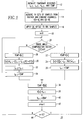
- step 12 sequentially samples the values of each of the voltage and current waveforms from those channels at a rate of about 512 samples per AC cycle. Although an example sample rate is disclosed, a wide range of suitable smaller or larger sample rates may be employed.
- a predetermined direct current (DC) offset per channel may be applied to the samples.
- this corrects for any known DC offset errors in the acquisition circuit (not shown) for each of the channels.
- an integer, n is set to zero.
- CF phase angle compensation factor
- the first of the current samples, I[n] is saved in the temporary register, Temp.
- the temporary register, I n-1 is set equal to the temporary register, Temp.
- the phase angle compensation factor (CF) has an absolute value that is smaller than one.
- the first of the current samples, I[n] is saved in the temporary register, Temp.
- the temporary register, I n-2 is set equal to the temporary register, I n-1 .
- the temporary register, I n-1 is set equal to the temporary register, Temp.
- the temporary register, Temp is set equal to the first of the voltage samples, V[n].
- the first voltage sample, V[n] is set equal to the temporary register, V n-1 .
- the temporary register, V n-1 is set equal to the temporary register, Temp.
- the integer, n is incremented.
- the routine 10 adjusts the sampled values of the current AC waveform to correspond with the sampled values of the voltage AC waveform by interpolating, at 24, between a corresponding one of the sampled values of the current AC waveform and a preceding sampled value of the current AC waveform, when the phase angle compensation factor (CF) is positive, or by interpolating, at 30, between the preceding sampled value and a sampled value of the current AC waveform preceding the preceding sampled value, when the phase angle compensation factor (CF) is negative.
- this will cause an error in the first current sample if CF is positive, or an error in the first and second samples if CF is negative. This error is insignificant in meter applications and happens only on start up or power up. Alternatively, the first two current samples may be ignored.
- FIG. 2 shows a flowchart of a calibration routine 50 for calculating the phase angle compensation factor (CF) of Figure 1.
- 2400 sets of digital samples are acquired from the voltage and current channels (not shown) and are stored in a voltage array 53 and a current array 54.
- the actual phase error between a voltage channel and the corresponding current channel is determined by preferably inputting pure in-phase sinusoidal signals into the voltage and current channels.
- a predetermined DC offset per channel may be applied to each of the samples in the arrays 53,54. Preferably, this corrects for any known DC offset errors in the acquisition circuit (not shown) for each of the channels.
- phase angle compensation factor This phase angle compensation factor (CF) is stored and employed, as was discussed above in connection with Figure 1, in order to determine how far to interpolate between the current digital samples in the array 54.
- Figure 3 shows an example plot 70 of a portion of a current AC waveform (I) including application of the phase angle compensation factor (CF) of Figure 1.
- This compensates for the relative phase shift of one or more current channels (not shown) with respect to corresponding one or more voltage channels (not shown) associated with the determination of electrical power and/or energy.
- the effect of phase errors between the current and voltage channels is corrected by linearly interpolating a synthesized sample time between adjacent current digital samples, such as those at times n and n-1, or between those at times n-1 and n-2.
- the compensation routine 10 of Figure 1 linearly interpolates between adjacent digital samples. Specifically, three digital samples are employed, in order to provide a range of+/-1 sample time (i.e ., about +/-0.7 degree at 512 samples/cycle). If the corresponding voltage waveform (not shown) is digitally sampled at sample time "n-1", then the three corresponding current digital samples are at sample times "n", "n-1" and "n-2".
- phase error is preferably measured and the result is stored, as was discussed above in connection with Figure 2, and the stored result is employed in real time, as was discussed above in connection with Figure 1.
- the worst case error between the actual digital sample, if in phase, and the corrected digital sample is about 0.12%. This error decreases with increases in the sampling rate.
- Figures 4A-4B show a flowchart of an auto-calibration routine 80 of a meter (not shown).
- standard voltage and current waveforms (not shown) are input to the meter.
- the standard voltage and current waveforms e.g ., without limitation, 110 VAC at 60 Hz; 10 A at 60 Hz
- a command e.g ., a suitable signal, such as, for example, a digital signal; a serial port signal; a data link signal; an input from a user interface
- the routine 80 acquires 2400 sets of current and voltage digital samples and applies DC offsets thereto.
- phase angle compensation factor (CF) is determined from Equation 6: wherein: i is an integer between 1 and j; and ZeroCrossingCount is an integer count, j, of voltage or current zero crossings as determined at steps 90 or 95.
- the meter auto-calibration routine 80 sends the compensation factor (CF) 103 to the meter sub-system 104, which saves and applies, at 106, the compensation factor 103 to periodically acquired digital current samples (not shown).
- CF compensation factor
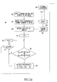
- Figures 5A-5B show a flowchart of an external calibration system routine 80' for calibrating a meter 104'.
- the routine 80' is similar to the routine 80 of Figures 4A-4B, except that the routine 80' is executed by an external calibration system 108, while the auto-calibration routine 80 is internal to the meter (not shown) associated with the meter sub-system 104 of Figures 4A-4B, and except as shown by different reference characters in Figures 5A-5B. For simplicity of disclosure, only those different reference characters are discussed with respect to Figures 5A-5B.
- a command (e.g ., a suitable signal, such as, for example, a digital signal; a serial port signal; a data link signal) is output from the external calibration system 108 over a suitable port 110 (e.g ., without limitation, a parallel port; a serial port; a data link; a communication network) to the meter 104' to start the calibration.
- a suitable port 110 e.g ., without limitation, a parallel port; a serial port; a data link; a communication network
- a meter routine 86' acquires 2400 sets of current and voltage digital samples and applies DC offsets thereto.
- the external calibration system 108 receives the 2400 sets of digital samples from the meter 104'.
- the external calibration system 108 sends such compensation factor over the port 110 to the meter 104', which saves and applies, at 106', the compensation factor 103' to the periodically acquired digital current samples (not shown).
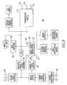
- Figure 6 shows a meter 120 including a processor 122 employing a phase angle compensation factor (CF) 124.
- the meter 120 further includes one or more first inputs 125 adapted to receive one or more first AC waveforms 126 ( e.g ., without limitation, voltage waveforms), and one or more second inputs 127 adapted to receive one or more second AC waveforms 128 ( e.g ., without limitation, current waveforms).
- An analog to digital converter circuit (ADC) 130 is adapted to sequentially sample and convert received first AC waveforms 132 to a plurality of first digital values 134 and is adapted to sequentially sample and convert received second AC waveforms 136 to a plurality of second digital values 138.
- ADC analog to digital converter circuit
- the processor 122 includes a routine 140 adapted to receive and process the first and second digital values 134,138 from the ADC 130.
- the routine 140 cooperates with a phase compensation routine 142 (e.g ., which may be the same as or similar to the compensation routine 10 of Figure 1) having the phase angle compensation factor (CF) 124, in order to compensate for phase differences between the sampled values 134,138.
- a phase compensation routine 142 e.g ., which may be the same as or similar to the compensation routine 10 of Figure 1
- the routine 140 and/or the ADC 130 may preferably include suitable DC offset and/or gain adjustments for the signals 134,138.
- the processor 122 further includes a calibration routine 144 (e.g., which may be the same as or similar to the auto-calibration routine 80 of Figures 4A-4B) adapted to calibrate the phase angle compensation factor (CF) 124.
- the calibration routine 144 is executed at power up or start up (e.g ., reset) and/or at any time responsive to a suitable command 146 received from port 148.
- the routine 140 may determine power and/or energy values 150 for display on display 151 (e.g ., a local or remote display).
- FIG. 7 another meter 120' including a processor 122' employing the phase angle compensation factor (CF) 124 is shown. Except as discussed, below, the meter 120' and processor 122' are the same as the respective meter 120 and processor 122 of Figure 6.
- the processor 122' instead of the phase compensation routine 142 of Figure 6, the processor 122' includes one or both of a first phase compensation routine 142' and a second different phase compensation routine 142''.
- the first compensation routine 142' (e.g ., similar to the compensation routine 10 of Figure 1, but excluding steps 28,30,32,34) is employed when the phase angle compensation factor 124 is positive and the second different compensation routine 142" (e.g ., similar to the compensation routine 10 of Figure 1, but excluding steps 22,24,26) is employed when the phase angle compensation factor 124 is negative.
- Figure 8 shows another meter 160 including processors 162 and 170 employing a phase angle compensation factor (CF) 164.
- the meter 160 is adapted to cooperate with an external calibration system, such as the system 108 of Figures 5A.
- the processor 162 includes an acquisition routine 166 adapted to receive and save a plurality of first and second digital calibration values 167 from an analog to digital converter 168.
- the acquisition routine 166 is executed at power up or start up of the meter 160 or at any time with a proper command responsive to a command 172 from the external calibration system 108 as received by a communication sub-system 174.
- the command 172 is communicated to the processor 170 through the processor circuit 162.
- the processor 170 communicates those through the host processor circuit 162 to the communication sub-system 174, which outputs those values in a message 176 to the external calibration system 108 of Figure 5A.
- the external calibration system 108 determines an external phase angle compensation factor 178, which is received by the communication sub-system 174.
- the external compensation factor 178 is communicated to the processor 170 through the host processor 162.
- the host processor 162 saves the externally determined compensation factor 178 as the local compensation factor (CF) 164 and sends the same to the processor 170 to compensate the signals.
- CF local compensation factor
- the processor 170 also includes a routine 180 employing the phase angle compensation factor (CF) 164, in order to compensate for phase differences between sampled values 182 and 184 from respective first and second AC waveforms 126 and 128.
- the routine 180 may be the same as or similar to the routines 140,142 of Figure 6.
- the communication sub-system 174 includes one or more suitable communication ports.
- phase compensation techniques provide digital precision for phase compensation without the hardware requirements of analog adjustment, relatively high-speed sampling and relatively complicated processing. This provides digital accuracy with relatively minimal processing.
- Figures 1 and 3 show phase compensation being applied to the current AC signals, such compensation may alternatively be applied to voltage AC signals.
Landscapes
- Physics & Mathematics (AREA)
- General Physics & Mathematics (AREA)
- Measurement Of Current Or Voltage (AREA)
- Measuring Phase Differences (AREA)
Abstract
Description
Vn is the voltage digital value at sample n; and
Vn-1 is the preceding voltage digital value at sample n-1, except for n = 0, wherein
Vn-1 = 0.
In is the current digital value at sample n; and
In-1 is the preceding current digital value at sample n-1, except for n = 0, wherein
In-1 = 0.

i is an integer between 1 and j; and
ZeroCrossingCount is an integer count, j, of voltage or current zero crossings as determined at
Claims (22)
- A method of compensating for phase differences between sampled values of first and second alternating current waveforms, said method comprising:employing a phase angle compensation factor;sequentially sampling a plurality of values of each of said first and second alternating current waveforms; andadjusting the sampled values of said second alternating current waveform to correspond with the sampled values of said first alternating current waveform by employing, for a corresponding one of said sampled values of said second alternating current waveform, a preceding sampled value of said second alternating current waveform plus the product of: (i) said phase angle compensation factor and (ii) the difference between said corresponding one of said sampled values and said preceding sampled value, when said phase angle compensation factor is positive, oralternatively adjusting the sampled values of said second alternating current waveform to correspond with the sampled values of said first alternating current waveform by employing, for said corresponding one of said sampled values, said preceding sampled value minus the product of: (i) the sum of one plus said phase angle compensation factor and (ii) the difference between said preceding sampled value and the sampled value of said second alternating current waveform preceding said preceding sampled value, when said phase angle compensation factor is negative.
- The method of Claim 1 further comprising:employing a meter;receiving said first and second alternating current waveforms at said meter;applying said phase angle compensation factor at said meter; andemploying a circuit internal to said meter to calibrate said phase angle compensation factor.
- The method of Claim 1 further comprising:employing a meter;receiving said first and second alternating current waveforms at said meter;applying said phase angle compensation factor at said meter; andemploying a circuit external to said meter to calibrate said phase angle compensation factor.
- The method of Claim 1 further comprising:employing as said first alternating current waveform a voltage alternating current waveform; andemploying as said second alternating current waveform a current alternating current waveform.
- The method of Claim 1 further comprising:sequentially sampling the values of each of said first and second alternating current waveforms at a rate of about 512 samples per alternating current cycle; andemploying said phase angle compensation factor, which has an absolute value that is smaller than one.
- The method of Claim 1 further comprising:acquiring a plurality of samples of said first and second alternating current waveforms before applying compensation to the sampled values of said second alternating current waveform.
- The method of Claim 1 further comprising:applying a direct current offset to the samples of said first and second alternating current waveforms before applying compensation to the sampled values of said second alternating current waveform.
- The method of Claim 1 further comprising:acquiring a plurality of sets of voltage samples and current samples as sampled values of each of said first and second alternating current waveforms;determining a plurality of zero crossings in said voltage samples;calculating a plurality of zero crossing sample times for said voltage samples;determining a plurality of zero crossings in said current samples;calculating a plurality of zero crossing sample times for said current samples;calculating a plurality of differences between the zero crossing sample times for said voltage samples and the zero crossing sample times for said current samples; andaveraging said differences to provide said phase angle compensation factor.
- The method of Claim 8 further comprising:applying a direct current offset to said voltage samples and said current samples before determining the zero crossings in said voltage samples and before determining the zero crossings in said current samples.
- The method of Claim 8 further comprising:incrementing and storing a count for each of said sets of voltage samples and current samples;calculating the zero crossing sample times for said voltage samples by employing, for a corresponding one of said zero crossing sample times and a corresponding one of said voltage samples, the stored count of said corresponding one of said voltage samples immediately before a corresponding one of said zero crossings plus the voltage of the voltage sample immediately before said corresponding one of said zero crossings divided by the difference between: (i) said voltage of the voltage sample immediately before said corresponding one of said zero crossings and (ii) the voltage of the voltage sample immediately after said corresponding one of said zero crossings; andcalculating the zero crossing sample times for said current samples by employing, for a corresponding one of said zero crossing sample times and a corresponding one of said current samples, the stored count of said corresponding one of said current samples immediately before a corresponding one of said zero crossings plus the current of the current sample immediately before said corresponding one of said zero crossings divided by the difference between: (i) said current of the current sample immediately before said corresponding one of said zero crossings and (ii) the current of the current sample immediately after said corresponding one of said zero crossings.
- The method of Claim 10 further comprisingdetermining the count of one of said voltage zero crossings and said current zero crossings;determining a plurality of differences between each of said zero crossing sample times for said voltage samples and corresponding ones of said zero crossing sample times for said current samples;summing said differences between each of said zero crossing sample times for said voltage samples and corresponding ones of said zero crossing sample times for said current samples; anddividing the sum of said differences by said count of one of said voltage zero crossings and said current zero crossings to determine said phase angle compensation factor.
- A meter apparatus comprising:a first input adapted to receive at least one first alternating current waveform;a second input adapted to receive at least one second alternating current waveform;an analog to digital converter circuit adapted to sequentially sample and convert said received at least one first alternating current waveform to a plurality of first digital values and adapted to sequentially sample and convert said received at least one second alternating current waveform to a plurality of second digital values;a processor adapted to receive and process the first and second digital values from said analog to digital converter circuit, said processor including a compensation routine having a phase angle compensation factor, said compensation routine being adapted to adjust said second digital values to correspond with said first digital values by employing, for a corresponding one of said second digital values, a preceding one of said second digital values plus the product of: (i) said phase angle compensation factor and (ii) the difference between said corresponding one of said second digital values and said preceding one of said second digital values, when said phase angle compensation factor is positive, or said routine being adapted to alternatively adjust said second digital values to correspond with said first digital values by employing, for said corresponding one of said second digital values, said preceding one of said second digital values minus the product of: (i) the sum of one plus said phase angle compensation factor and (ii) the difference between said preceding one of said second digital values and the second digital value preceding said preceding one of said second digital values, when said phase angle compensation factor is negative, in order to compensate for phase differences between said first and second digital values.
- The meter apparatus of Claim 12 wherein said processor further includes a calibration routine adapted to receive and save a plurality of first and second digital calibration values from said analog to digital converter circuit, to communicate said saved first and second digital calibration values to an external calibration circuit, and to receive from said external calibration circuit said phase angle compensation factor.
- The meter apparatus of Claim 12 wherein said processor further includes a calibration routine adapted to calibrate said phase angle compensation factor.
- The meter apparatus of Claim 14 wherein said calibration routine is adapted to acquire a plurality of sets of voltage samples and current samples as sampled values of each of said first and second alternating current waveforms, determine a plurality of zero crossings in said voltage samples, calculate a plurality of zero crossing sample times for said voltage samples, determine a plurality of zero crossings in said current samples, calculate a plurality of zero crossing sample times for said current samples, calculate a plurality of differences between the zero crossing sample times for said voltage samples and the zero crossing sample times for said current samples, and average said differences to provide said phase angle compensation factor.
- The meter apparatus of Claim 15 wherein said calibration routine is further adapted to apply a direct current offset to said voltage samples and said current samples before determining the zero crossings in said voltage samples and before determining the zero crossings in said current samples.
- The meter apparatus of Claim 15 wherein said calibration routine is further adapted to increment and store a count for each of said sets of voltage samples and current samples, calculate the zero crossing sample times for said voltage samples by employing, for a corresponding one of said zero crossing sample times and a corresponding one of said voltage samples, the stored count of said corresponding one of said voltage samples immediately before a corresponding one of said zero crossings plus the voltage of the voltage sample immediately before said corresponding one of said zero crossings divided by the difference between: (i) said voltage of the voltage sample immediately before said corresponding one of said zero crossings and (ii) the voltage of the voltage sample immediately after said corresponding one of said zero crossings, and calculate the zero crossing sample times for said current samples by employing, for a corresponding one of said zero crossing sample times and a corresponding one of said current samples, the stored count of said corresponding one of said current samples immediately before a corresponding one of said zero crossings plus the current of the current sample immediately before said corresponding one of said zero crossings divided by the difference between: (i) said current of the current sample immediately before said corresponding one of said zero crossings and (ii) the current of the current sample immediately after said corresponding one of said zero crossings.
- The meter apparatus of Claim 17 wherein said calibration routine is further adapted to determine the count of one of said voltage zero crossings and said current zero crossings, determine a plurality of differences between each of said zero crossing sample times for said voltage samples and corresponding ones of said zero crossing sample times for said current samples, sum said differences between each of said zero crossing sample times for said voltage samples and corresponding ones of said zero crossing sample times for said current samples, and divide the sum of said differences by said count of one of said voltage zero crossings and said current zero crossings to determine said phase angle compensation factor.
- The meter apparatus of Claim 12 wherein said processor further includes a routine to calculate energy from said first digital values and said adjusted second digital values.
- The meter apparatus of Claim 12 wherein the compensation routine of said processor is a first compensation routine when said phase angle compensation factor is positive and a second different compensation routine when said phase angle compensation factor is negative.
- A method of compensating for phase differences between sampled values of first and second alternating current waveforms, said method comprising:employing a phase angle compensation factor;sequentially sampling a plurality of values of each of said first and second alternating current waveforms; andadjusting the sampled values of said second alternating current waveform to correspond with the sampled values of said first alternating current waveform by interpolating between a corresponding one of said sampled values of said second alternating current waveform and a preceding sampled value of said second alternating current waveform, when said phase angle compensation factor is positive, or by interpolating between the preceding sampled value and a sampled value of said second alternating current waveform preceding said preceding sampled value, when said phase angle compensation factor is negative.
- The method of Claim 21 further comprising:interpolating between said corresponding one of said sampled values of said second alternating current waveform and said preceding sampled value of said second alternating current waveform by a percentage defined by said positive phase angle compensation factor; andalternatively interpolating between the preceding sampled value and said sampled value of said second alternating current waveform preceding said preceding sampled value by a percentage defined by said negative phase angle compensation factor.
Applications Claiming Priority (2)
| Application Number | Priority Date | Filing Date | Title |
|---|---|---|---|
| US10/865,476 US6975951B1 (en) | 2004-06-10 | 2004-06-10 | Meter apparatus and method for phase angle compensation employing linear interpolation of digital signals |
| US865476 | 2004-06-10 |
Publications (3)
| Publication Number | Publication Date |
|---|---|
| EP1605275A2 true EP1605275A2 (en) | 2005-12-14 |
| EP1605275A3 EP1605275A3 (en) | 2006-05-24 |
| EP1605275B1 EP1605275B1 (en) | 2010-08-04 |
Family
ID=34937374
Family Applications (1)
| Application Number | Title | Priority Date | Filing Date |
|---|---|---|---|
| EP05012551A Ceased EP1605275B1 (en) | 2004-06-10 | 2005-06-10 | Electronic meter digital phase compensation |
Country Status (4)
| Country | Link |
|---|---|
| US (1) | US6975951B1 (en) |
| EP (1) | EP1605275B1 (en) |
| CA (1) | CA2509473A1 (en) |
| DE (1) | DE602005022652D1 (en) |
Cited By (1)
| Publication number | Priority date | Publication date | Assignee | Title |
|---|---|---|---|---|
| CN102645567A (en) * | 2010-10-21 | 2012-08-22 | 特克特朗尼克公司 | Zero ampere level current data correction for power device under test |
Families Citing this family (11)
| Publication number | Priority date | Publication date | Assignee | Title |
|---|---|---|---|---|
| US8165832B1 (en) * | 2008-11-12 | 2012-04-24 | Ixys Ch Gmbh | Wall plug power monitor |
| US9335352B2 (en) * | 2009-03-13 | 2016-05-10 | Veris Industries, Llc | Branch circuit monitor power measurement |
| US8368334B2 (en) * | 2009-11-18 | 2013-02-05 | Standard Microsystems Corporation | Brushless, three phase motor drive |
| US8942942B2 (en) | 2010-07-23 | 2015-01-27 | Caterpillar Inc. | Generator set calibration controller |
| US8478550B2 (en) | 2010-07-23 | 2013-07-02 | Caterpillar Inc. | Generator set calibration controller |
| US10132663B2 (en) * | 2015-04-30 | 2018-11-20 | Goodrich Corporation | Self-calibrating linear voltage differential transformer demodulator |
| US11320495B2 (en) * | 2019-08-30 | 2022-05-03 | Schweitzer Engineering Laboratories, Inc. | Current-based directional element in a power delivery system |
| US12025679B2 (en) | 2020-08-28 | 2024-07-02 | Schweitzer Engineering Laboratories, Inc | Integrating memory dropout timer |
| KR102822473B1 (en) * | 2020-12-02 | 2025-06-19 | 현대모비스 주식회사 | Apparatus and method for compensation for offset in switching current sensing |
| CN115421088B (en) * | 2022-08-11 | 2025-06-13 | 福建星云电子股份有限公司 | A measurement equipment loop calibration method |
| CN120254594B (en) * | 2025-06-05 | 2025-09-16 | 东方电子股份有限公司 | Initial phase angle high-precision measurement method and measurement device based on automatic correction of double-point angle difference |
Family Cites Families (8)
| Publication number | Priority date | Publication date | Assignee | Title |
|---|---|---|---|---|
| DE2630959C2 (en) * | 1976-07-07 | 1986-04-30 | Heliowatt Werke Elektrizitäts- Gesellschaft mbH, 1000 Berlin | Kilowatt hour meter with static measuring mechanism |
| US4996871A (en) * | 1989-06-02 | 1991-03-05 | Micro Motion, Inc. | Coriolis densimeter having substantially increased noise immunity |
| US5151866A (en) * | 1990-03-30 | 1992-09-29 | The Dow Chemical Company | High speed power analyzer |
| US6043642A (en) * | 1996-08-01 | 2000-03-28 | Siemens Power Transmission & Distribution, Inc. | Watt-hour meter with communication on diagnostic error detection |
| US6735535B1 (en) * | 2000-05-05 | 2004-05-11 | Electro Industries/Gauge Tech. | Power meter having an auto-calibration feature and data acquisition capabilities |
| US6636028B2 (en) * | 2001-06-01 | 2003-10-21 | General Electric Company | Electronic electricity meter configured to correct for transformer inaccuracies |
| US6748344B2 (en) * | 2002-04-29 | 2004-06-08 | Eaton Corporation | Method and apparatus employing a scaling factor for measuring and displaying an electrical parameter of an electrical system |
| US6943714B2 (en) * | 2002-08-19 | 2005-09-13 | Tdk Semiconductor Corporation | Method and apparatus of obtaining power computation parameters |
-
2004
- 2004-06-10 US US10/865,476 patent/US6975951B1/en not_active Expired - Lifetime
-
2005
- 2005-06-08 CA CA002509473A patent/CA2509473A1/en not_active Abandoned
- 2005-06-10 DE DE602005022652T patent/DE602005022652D1/en not_active Expired - Lifetime
- 2005-06-10 EP EP05012551A patent/EP1605275B1/en not_active Ceased
Cited By (2)
| Publication number | Priority date | Publication date | Assignee | Title |
|---|---|---|---|---|
| CN102645567A (en) * | 2010-10-21 | 2012-08-22 | 特克特朗尼克公司 | Zero ampere level current data correction for power device under test |
| CN102645567B (en) * | 2010-10-21 | 2016-08-03 | 特克特朗尼克公司 | For the method and apparatus correcting the current data sample representing current signal |
Also Published As
| Publication number | Publication date |
|---|---|
| US6975951B1 (en) | 2005-12-13 |
| US20050288884A1 (en) | 2005-12-29 |
| EP1605275A3 (en) | 2006-05-24 |
| DE602005022652D1 (en) | 2010-09-16 |
| EP1605275B1 (en) | 2010-08-04 |
| CA2509473A1 (en) | 2005-12-10 |
Similar Documents
| Publication | Publication Date | Title |
|---|---|---|
| CN100523832C (en) | Method and apparatus for phase compensation in an electronic energy meter | |
| US6943714B2 (en) | Method and apparatus of obtaining power computation parameters | |
| US8519875B2 (en) | System and method for background calibration of time interleaved analog to digital converters | |
| US6975951B1 (en) | Meter apparatus and method for phase angle compensation employing linear interpolation of digital signals | |
| US6377037B1 (en) | Watt-hour meter with digital per-phase power factor compensation | |
| US7148828B2 (en) | System and method for timing calibration of time-interleaved data converters | |
| JP3863977B2 (en) | A / D converter correction method and apparatus | |
| US8125361B2 (en) | Digital-to-analog converter (DAC) calibration system | |
| US7741982B2 (en) | Estimation of timing errors in a time-interleaved analog to digital converter system | |
| CN110244116B (en) | DC instantaneous power measurement circuit and quasi-synchronous calculation method | |
| US20030011353A1 (en) | System and method for calibration of data in an electric power monitoring system | |
| GB2408107A (en) | Electrical power meter with phase compensation | |
| US6944569B2 (en) | Method and apparatus for generating an electronic test signal | |
| EP0525428B1 (en) | Digital protective relay apparatus | |
| US20200011940A1 (en) | Hall sensor with interleaved and/or sliding averaged/summed spinning phases | |
| US20120084035A1 (en) | System and method for frequency measurement based on quadratic forms | |
| CA2422504C (en) | Methods and apparatus for analog-to-digital conversion | |
| CN1671053A (en) | Method and related device for correcting DC offset of digital-to-analog converter | |
| KR20050103506A (en) | Digitizer device, waveform generation device, conversion method, waveform generation method, and recording medium containing the program thereof | |
| JP3317557B2 (en) | Transmission line constant measuring device and method for improving measurement accuracy | |
| US6304202B1 (en) | Delay correction system and method for a voltage channel in a sampled data measurement system | |
| JP2982612B2 (en) | PQ calculation correction method | |
| CN105652082B (en) | High-precision electrical signal frequency measurement method and device | |
| JP2002300036A (en) | Method and apparatus for measuring amplification factor ratio of signal normalizer | |
| CN117348036A (en) | A satellite navigation signal delay stability control method and system |
Legal Events
| Date | Code | Title | Description |
|---|---|---|---|
| PUAI | Public reference made under article 153(3) epc to a published international application that has entered the european phase |
Free format text: ORIGINAL CODE: 0009012 |
|
| AK | Designated contracting states |
Kind code of ref document: A2 Designated state(s): AT BE BG CH CY CZ DE DK EE ES FI FR GB GR HU IE IS IT LI LT LU MC NL PL PT RO SE SI SK TR |
|
| AX | Request for extension of the european patent |
Extension state: AL BA HR LV MK YU |
|
| PUAL | Search report despatched |
Free format text: ORIGINAL CODE: 0009013 |
|
| AK | Designated contracting states |
Kind code of ref document: A3 Designated state(s): AT BE BG CH CY CZ DE DK EE ES FI FR GB GR HU IE IS IT LI LT LU MC NL PL PT RO SE SI SK TR |
|
| AX | Request for extension of the european patent |
Extension state: AL BA HR LV MK YU |
|
| 17P | Request for examination filed |
Effective date: 20061122 |
|
| R17P | Request for examination filed (corrected) |
Effective date: 20061122 |
|
| AKX | Designation fees paid |
Designated state(s): DE FR GB |
|
| 17Q | First examination report despatched |
Effective date: 20071115 |
|
| GRAP | Despatch of communication of intention to grant a patent |
Free format text: ORIGINAL CODE: EPIDOSNIGR1 |
|
| GRAS | Grant fee paid |
Free format text: ORIGINAL CODE: EPIDOSNIGR3 |
|
| GRAA | (expected) grant |
Free format text: ORIGINAL CODE: 0009210 |
|
| AK | Designated contracting states |
Kind code of ref document: B1 Designated state(s): DE FR GB |
|
| REG | Reference to a national code |
Ref country code: GB Ref legal event code: FG4D |
|
| REF | Corresponds to: |
Ref document number: 602005022652 Country of ref document: DE Date of ref document: 20100916 Kind code of ref document: P |
|
| PLBE | No opposition filed within time limit |
Free format text: ORIGINAL CODE: 0009261 |
|
| STAA | Information on the status of an ep patent application or granted ep patent |
Free format text: STATUS: NO OPPOSITION FILED WITHIN TIME LIMIT |
|
| 26N | No opposition filed |
Effective date: 20110506 |
|
| REG | Reference to a national code |
Ref country code: DE Ref legal event code: R097 Ref document number: 602005022652 Country of ref document: DE Effective date: 20110506 |
|
| PGFP | Annual fee paid to national office [announced via postgrant information from national office to epo] |
Ref country code: GB Payment date: 20130529 Year of fee payment: 9 |
|
| GBPC | Gb: european patent ceased through non-payment of renewal fee |
Effective date: 20140610 |
|
| PG25 | Lapsed in a contracting state [announced via postgrant information from national office to epo] |
Ref country code: GB Free format text: LAPSE BECAUSE OF NON-PAYMENT OF DUE FEES Effective date: 20140610 |
|
| REG | Reference to a national code |
Ref country code: FR Ref legal event code: PLFP Year of fee payment: 12 |
|
| REG | Reference to a national code |
Ref country code: FR Ref legal event code: PLFP Year of fee payment: 13 |
|
| REG | Reference to a national code |
Ref country code: FR Ref legal event code: PLFP Year of fee payment: 14 |
|
| REG | Reference to a national code |
Ref country code: DE Ref legal event code: R082 Ref document number: 602005022652 Country of ref document: DE Ref country code: DE Ref legal event code: R081 Ref document number: 602005022652 Country of ref document: DE Owner name: EATON INTELLIGENT POWER LIMITED, IE Free format text: FORMER OWNER: EATON CORP., CLEVELAND, OHIO, US |
|
| PGFP | Annual fee paid to national office [announced via postgrant information from national office to epo] |
Ref country code: FR Payment date: 20220519 Year of fee payment: 18 Ref country code: DE Payment date: 20220518 Year of fee payment: 18 |
|
| REG | Reference to a national code |
Ref country code: DE Ref legal event code: R119 Ref document number: 602005022652 Country of ref document: DE |
|
| PG25 | Lapsed in a contracting state [announced via postgrant information from national office to epo] |
Ref country code: DE Free format text: LAPSE BECAUSE OF NON-PAYMENT OF DUE FEES Effective date: 20240103 |
|
| PG25 | Lapsed in a contracting state [announced via postgrant information from national office to epo] |
Ref country code: FR Free format text: LAPSE BECAUSE OF NON-PAYMENT OF DUE FEES Effective date: 20230630 |