EP1603105A2 - Method and apparatus for reducing charge injection in control of MEMS electrostatic actuator array - Google Patents
Method and apparatus for reducing charge injection in control of MEMS electrostatic actuator array Download PDFInfo
- Publication number
- EP1603105A2 EP1603105A2 EP05009243A EP05009243A EP1603105A2 EP 1603105 A2 EP1603105 A2 EP 1603105A2 EP 05009243 A EP05009243 A EP 05009243A EP 05009243 A EP05009243 A EP 05009243A EP 1603105 A2 EP1603105 A2 EP 1603105A2
- Authority
- EP
- European Patent Office
- Prior art keywords
- voltage
- gate
- semiconductor switch
- source
- control circuit
- Prior art date
- Legal status (The legal status is an assumption and is not a legal conclusion. Google has not performed a legal analysis and makes no representation as to the accuracy of the status listed.)
- Ceased
Links
- 238000002347 injection Methods 0.000 title claims abstract description 41
- 239000007924 injection Substances 0.000 title claims abstract description 41
- 238000000034 method Methods 0.000 title description 5
- 239000004065 semiconductor Substances 0.000 claims abstract description 40
- 239000003990 capacitor Substances 0.000 claims abstract description 27
- 238000009825 accumulation Methods 0.000 claims description 4
- 230000003247 decreasing effect Effects 0.000 description 5
- 238000010586 diagram Methods 0.000 description 5
- 230000008878 coupling Effects 0.000 description 4
- 238000010168 coupling process Methods 0.000 description 4
- 238000005859 coupling reaction Methods 0.000 description 4
- 230000000694 effects Effects 0.000 description 3
- 230000007246 mechanism Effects 0.000 description 3
- 230000002829 reductive effect Effects 0.000 description 3
- 238000004088 simulation Methods 0.000 description 3
- 230000008901 benefit Effects 0.000 description 2
- 238000004891 communication Methods 0.000 description 2
- 238000009499 grossing Methods 0.000 description 2
- 230000000670 limiting effect Effects 0.000 description 2
- 238000012986 modification Methods 0.000 description 2
- 230000004048 modification Effects 0.000 description 2
- 238000012544 monitoring process Methods 0.000 description 2
- 230000003071 parasitic effect Effects 0.000 description 2
- 238000013459 approach Methods 0.000 description 1
- 238000003491 array Methods 0.000 description 1
- 230000009286 beneficial effect Effects 0.000 description 1
- 230000008859 change Effects 0.000 description 1
- 230000000295 complement effect Effects 0.000 description 1
- 230000003750 conditioning effect Effects 0.000 description 1
- 238000010276 construction Methods 0.000 description 1
- 238000013461 design Methods 0.000 description 1
- 238000011161 development Methods 0.000 description 1
- 230000003292 diminished effect Effects 0.000 description 1
- 239000006185 dispersion Substances 0.000 description 1
- 230000006872 improvement Effects 0.000 description 1
- 229910044991 metal oxide Inorganic materials 0.000 description 1
- 150000004706 metal oxides Chemical class 0.000 description 1
- 230000003287 optical effect Effects 0.000 description 1
- 238000005192 partition Methods 0.000 description 1
- 230000008569 process Effects 0.000 description 1
- 230000009467 reduction Effects 0.000 description 1
- 239000007787 solid Substances 0.000 description 1
- 230000003068 static effect Effects 0.000 description 1
- 238000012360 testing method Methods 0.000 description 1
- 230000003313 weakening effect Effects 0.000 description 1
Images



Classifications
-
- G—PHYSICS
- G09—EDUCATION; CRYPTOGRAPHY; DISPLAY; ADVERTISING; SEALS
- G09G—ARRANGEMENTS OR CIRCUITS FOR CONTROL OF INDICATING DEVICES USING STATIC MEANS TO PRESENT VARIABLE INFORMATION
- G09G3/00—Control arrangements or circuits, of interest only in connection with visual indicators other than cathode-ray tubes
- G09G3/20—Control arrangements or circuits, of interest only in connection with visual indicators other than cathode-ray tubes for presentation of an assembly of a number of characters, e.g. a page, by composing the assembly by combination of individual elements arranged in a matrix no fixed position being assigned to or needed to be assigned to the individual characters or partial characters
- G09G3/34—Control arrangements or circuits, of interest only in connection with visual indicators other than cathode-ray tubes for presentation of an assembly of a number of characters, e.g. a page, by composing the assembly by combination of individual elements arranged in a matrix no fixed position being assigned to or needed to be assigned to the individual characters or partial characters by control of light from an independent source
- G09G3/3433—Control arrangements or circuits, of interest only in connection with visual indicators other than cathode-ray tubes for presentation of an assembly of a number of characters, e.g. a page, by composing the assembly by combination of individual elements arranged in a matrix no fixed position being assigned to or needed to be assigned to the individual characters or partial characters by control of light from an independent source using light modulating elements actuated by an electric field and being other than liquid crystal devices and electrochromic devices
-
- G—PHYSICS
- G09—EDUCATION; CRYPTOGRAPHY; DISPLAY; ADVERTISING; SEALS
- G09G—ARRANGEMENTS OR CIRCUITS FOR CONTROL OF INDICATING DEVICES USING STATIC MEANS TO PRESENT VARIABLE INFORMATION
- G09G2300/00—Aspects of the constitution of display devices
- G09G2300/08—Active matrix structure, i.e. with use of active elements, inclusive of non-linear two terminal elements, in the pixels together with light emitting or modulating elements
- G09G2300/0809—Several active elements per pixel in active matrix panels
-
- G—PHYSICS
- G09—EDUCATION; CRYPTOGRAPHY; DISPLAY; ADVERTISING; SEALS
- G09G—ARRANGEMENTS OR CIRCUITS FOR CONTROL OF INDICATING DEVICES USING STATIC MEANS TO PRESENT VARIABLE INFORMATION
- G09G2300/00—Aspects of the constitution of display devices
- G09G2300/08—Active matrix structure, i.e. with use of active elements, inclusive of non-linear two terminal elements, in the pixels together with light emitting or modulating elements
- G09G2300/0809—Several active elements per pixel in active matrix panels
- G09G2300/0814—Several active elements per pixel in active matrix panels used for selection purposes, e.g. logical AND for partial update
-
- G—PHYSICS
- G09—EDUCATION; CRYPTOGRAPHY; DISPLAY; ADVERTISING; SEALS
- G09G—ARRANGEMENTS OR CIRCUITS FOR CONTROL OF INDICATING DEVICES USING STATIC MEANS TO PRESENT VARIABLE INFORMATION
- G09G2300/00—Aspects of the constitution of display devices
- G09G2300/08—Active matrix structure, i.e. with use of active elements, inclusive of non-linear two terminal elements, in the pixels together with light emitting or modulating elements
- G09G2300/0809—Several active elements per pixel in active matrix panels
- G09G2300/0833—Several active elements per pixel in active matrix panels forming a linear amplifier or follower
- G09G2300/0838—Several active elements per pixel in active matrix panels forming a linear amplifier or follower with level shifting
-
- G—PHYSICS
- G09—EDUCATION; CRYPTOGRAPHY; DISPLAY; ADVERTISING; SEALS
- G09G—ARRANGEMENTS OR CIRCUITS FOR CONTROL OF INDICATING DEVICES USING STATIC MEANS TO PRESENT VARIABLE INFORMATION
- G09G2300/00—Aspects of the constitution of display devices
- G09G2300/08—Active matrix structure, i.e. with use of active elements, inclusive of non-linear two terminal elements, in the pixels together with light emitting or modulating elements
- G09G2300/088—Active matrix structure, i.e. with use of active elements, inclusive of non-linear two terminal elements, in the pixels together with light emitting or modulating elements using a non-linear two-terminal element
-
- G—PHYSICS
- G09—EDUCATION; CRYPTOGRAPHY; DISPLAY; ADVERTISING; SEALS
- G09G—ARRANGEMENTS OR CIRCUITS FOR CONTROL OF INDICATING DEVICES USING STATIC MEANS TO PRESENT VARIABLE INFORMATION
- G09G2320/00—Control of display operating conditions
- G09G2320/02—Improving the quality of display appearance
- G09G2320/0219—Reducing feedthrough effects in active matrix panels, i.e. voltage changes on the scan electrode influencing the pixel voltage due to capacitive coupling
-
- G—PHYSICS
- G09—EDUCATION; CRYPTOGRAPHY; DISPLAY; ADVERTISING; SEALS
- G09G—ARRANGEMENTS OR CIRCUITS FOR CONTROL OF INDICATING DEVICES USING STATIC MEANS TO PRESENT VARIABLE INFORMATION
- G09G3/00—Control arrangements or circuits, of interest only in connection with visual indicators other than cathode-ray tubes
- G09G3/20—Control arrangements or circuits, of interest only in connection with visual indicators other than cathode-ray tubes for presentation of an assembly of a number of characters, e.g. a page, by composing the assembly by combination of individual elements arranged in a matrix no fixed position being assigned to or needed to be assigned to the individual characters or partial characters
- G09G3/34—Control arrangements or circuits, of interest only in connection with visual indicators other than cathode-ray tubes for presentation of an assembly of a number of characters, e.g. a page, by composing the assembly by combination of individual elements arranged in a matrix no fixed position being assigned to or needed to be assigned to the individual characters or partial characters by control of light from an independent source
- G09G3/3433—Control arrangements or circuits, of interest only in connection with visual indicators other than cathode-ray tubes for presentation of an assembly of a number of characters, e.g. a page, by composing the assembly by combination of individual elements arranged in a matrix no fixed position being assigned to or needed to be assigned to the individual characters or partial characters by control of light from an independent source using light modulating elements actuated by an electric field and being other than liquid crystal devices and electrochromic devices
- G09G3/3466—Control arrangements or circuits, of interest only in connection with visual indicators other than cathode-ray tubes for presentation of an assembly of a number of characters, e.g. a page, by composing the assembly by combination of individual elements arranged in a matrix no fixed position being assigned to or needed to be assigned to the individual characters or partial characters by control of light from an independent source using light modulating elements actuated by an electric field and being other than liquid crystal devices and electrochromic devices based on interferometric effect
Definitions
- the present invention relates generally to a MEMS (Micro-Electro-Mechanical Systems) and more specifically to a control arrangement for a MEMS actuator which reduces charge errors and which allows more precise control of the MEMS actuator position and increases control range.
- MEMS Micro-Electro-Mechanical Systems
- MOS Metal Oxide Semiconductor
- Fig. 1 is a schematic depiction of an embodiment of the invention showing a variable capacitor and a charge injection control circuit which is connected to the variable capacitor through a semiconductor device such as transistor and which controls the development of charge on the upper of the two electrodes.
- Fig. 2 is a circuit diagram showing a first embodiment of an injection control circuit which is applied to the arrangement illustrated in Fig. 1.
- Fig. 3 is a circuit diagram showing a second embodiment of an injection control circuit.
- Figs. 4A - 4C graphically depict operational characteristics of the circuit arrangement shown in Fig. 2 (first embodiment).
- Figs. 5A - 5C graphically depict the operational characteristics of the circuit arrangement shown in Fig. 3 (second embodiment).
- Fig. 6 is a circuit diagram showing a third embodiment of the injection control circuit.
- Figs. 7A - 7C graphically depict operation characteristics of the circuit arrangement shown in Fig. 6 (third embodiment).
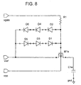
- Fig. 8 is a circuit diagram of a fourth embodiment of the injection control circuit which includes one or more diodes in each array of sub-circuit and which limits the "on” and “off” gate voltages of the MOS switch.
- Fig. 9 graphically depict the operation characteristics of the circuit arrangement shown in Fig. 8 (fourth embodiment) on charge injection.
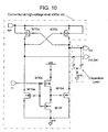
- Fig. 10 is a circuit diagram which shows an example of a modified level shifter circuit which comprises an embodiment of the invention and which can be used with the other embodiments.
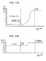
- Figs. 11A and 11B are graphs which show operation characteristics of an unoptimized level shifter circuit of the type shown in Fig. 10.
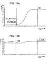
- Figs. 12A and 12B are graphs which show operation characteristics of a level shifter circuit modified in the manner illustrated in Fig. 10.
- Fig. 1 shows an embodiment of the invention.
- a variable capacitor C1 consists of a bottom fixed plate (which can be grounded), and a movable top plate which is suspended by flexure beams (not shown).
- the variable gap A between the two plates is controlled by controlling the charge on the upper or top plate.
- an injection control circuit is connected with the upper plate via a solid state switch.
- this arrangement comprises a variable capacitor having a fixed plate and movable plate disposed in predetermined spatial relationship with respect to the fixed plate; and a semiconductor switch which has a source, a drain and a gate, which is associated with a selected one of the fixed and movable plates of the capacitor and which is arranged to selectively connect the selected one of the fixed and movable plates with a voltage source.
- a charge injection control circuit is associated with the semiconductor switch so as to attenuate current injection into the selected one of the fixed and movable plates of the capacitor.
- Fig. 1 C1 denotes the variable capacitor (flexures are not shown).
- M1 is an analog switch formed by an NMOS device, a PMOS device, or NMOS and PMOS devices.
- V_ref is an analog reference voltage.
- En is the enable signal which is generated by the charge injection control circuit. To "write" a charge to C1 and change Gap A, V_ref is established, and then M1 is turned on by En which is generated by the charge control circuit. After an appropriate time (a function of the circuit's electrical time constant), M1 is turned off.
- This process changes the amount of charge on C1 and induces the situation wherein the electrostatic charge which has accumulated on C1 draws the movable plate toward the fixed plate.
- the circuit of Fig. 1 is replicated N x M times, in N rows and M columns.
- En could be a row signal, for a total of N En signals, and V_ref could be a column signal for M V_ref signals.
- charge errors occur by way of two mechanisms. The first is due to channel charge, which must flow out from the channel region of the transistor to the drain and source junctions. The second charge is due to overlap capacitance between the gate and drain. The embodiments of the invention described here minimize these sources of charge error.
- each En row signal may be voltage level-shifted from a low voltage (5 V, for example) output from the control logic to a high-voltage (12 V, for example) signal appropriate for the array by means of a high-voltage level shifter circuit.
- the gates of the analog MOS switches in the array can experience voltage swings of 0-12 V, which can inject significant noise due to gate-drain coupling and channel charge injection. It is desired to limit the voltage swing on the gate of the MOS switch to reduce charge injection into the MEMS device. Embodiments that accomplish this are described below:
- the first and second embodiments of the charge injection control circuit are directed to reducing charge injection in MEMS electrostatic actuators by decreasing gate voltage swing on the drive transistor.
- these circuits comprise first and second semiconductor elements which are circuited with a gate of the semiconductor switches and which modify a gate signal which is applied to the gate in a manner wherein at least one of:
- Fig. 2 shows details of the first embodiment of the charge injection control circuit.
- this embodiment requires the addition of two devices to each array subcircuit to limit the "off" gate voltage of the MOS switch and slow the switch closure to the degree that instead of the charge beneath the gate being permitted to distribute 50/50 between the source and the drain, most of the charge is, due to the differential capacitance between the source and drain, permitted to drain off to the source side.
- M1b and C1b represent M1 and C1 of Fig. 1 respectively.
- M6b and M7b are used to condition the signal ngate_vb, which enables/disables MOS switch M1b.
- M1b PMOS
- M7b NMOS
- row_enb a high-voltage signal.
- M1b is on, the gate of M1b is driven to all the way to ground (0 V).
- M1b off instead of driving the gate of M1b to a full vpp, which would inject maximum coupling noise, the gate of M1b is only driven to vref by M6b.
- a gate voltage of vref is the minimum voltage required to fully turn M1b off.
- NMOS device for M6b has the added benefit of smoothing out (slowing) the turn-off voltage slope on ngate_vb, which reduces charge injection in M1b due to channel charge dispersion.
- Fig. 3 shows a second embodiment of the invention. This embodiment is also directed limiting the "off" gate voltage of the MOS switch and is such that M1c and C1c respectively represent M1 and C1 of Fig. 1.
- the signal/element designations which end in the letter “b” in Fig. 2 have corresponding designations wherein the letter “b” is replaced with the letter “c”.
- the letter "b” is replaced by the letter “d”.
- the high voltage signal row_enb in Fig. 2 becomes row_enc and row_end in Figs. 3 and 6 respectively.
- the signals row-en and row-en-bar are high voltage signals which are applied in accordance with the need to vary the gap A of the variable capacitors.
- M6c and M7c are used to condition the signal ngate_vc, which enables/disables NMOS switch M1c.
- M1c NMOS
- M7c PMOS
- row_en_barc a high-voltage signal.
- M1c on the gate of M1c is driven to a full high voltage vpp.
- M1c off instead of driving the gate of M1c to 0 V, which would inject maximum coupling noise, the gate of M1c is only driven to vref by M6c. Because the source of M1c is at vref, a gate voltage of vref is the minimum voltage required to fully turn M1c off.
- a PMOS device for M6c has the added benefit of smoothing out the voltage slope on ngate_vc, which reduces charge injection in M1c due to channel charge
- each of the traces labeled "Unoptimized” is a trace of the waveform of the drain of the PMOS switch, the gate of which is driven directly by the bottom waveform (or its complement, in this case).
- the "optimized” waveform uses the extra devices M6b and M7b to limit the voltage swing on the gate of the PMOS switch.
- 5.546 fC femto Coulomb
- 2.856 fC are injected onto the capacitive load.
- NMOS switch The circuit of Fig. 3 (NMOS switch) was simulated to demonstrate the advantageous effects of M6b and M6c on charge injection. The results are depicted graphically in Figs. 5A -5C.
- the waveform labeled "Unoptimized” in Fig. 5A is a trace of the waveform of the drain of the NMOS switch, the gate of which is driven directly by the waveform shown in Fig. 5C.
- the "optimized” waveform (Fig. 5B) uses the extra devices M6b and M7b to limit the voltage swing on the gate of the NMOS switch. In the unoptimized case, 2.565 fC are injected onto the capacitive load. In the optimized case, only 1.115 fC are injected onto the capacitive load.
- Fig. 6 shows a third embodiment of the charge injection control circuit. This embodiment is directed limiting both "on” and “off” gate voltages to the MOS switch and includes the addition of two devices and one or two reference voltages to each array subcircuit. The reference voltages can be common to the entire array and the embodiment utilizes a PMOS analog switch.
- the reference voltages v_gate_off and v_gate_on can be set depending on the range of voltages that will be used for vref. For example, v_gate_on could be set to approximately one volt below the minimum vref, and v_gate_off could be set to approximately the maximum vref, thus ensuring that the accumulation charge (when M1d is off) and inversion charge (when M1d is on) are minimized.
- Fig. 6 shows simulation results from the circuit of Figure 6.
- the bottom waveform is row_end
- the middle waveform is ngate_vd
- the top waveform is the voltage on C1d.
- Figs. 7A can be compared with those of the unoptimized case of Fig. 4A.
- 5.546 fC by way of example
- 1.445 fC by way of example only
- Fig. 8 shows a fourth embodiment of the invention which requires the addition of one or more diodes to each array sub circuit, as well as a resistor which may be implemented using an active device such as an NMOS or PMOS.
- This embodiment limits the "on” and “off” gate voltages of the MOS switch. In the case of a PMOS switch, the gate voltage of the switch can be limited to an acceptable range around vref by means of the circuit shown in this figure.
- the series diodes can be replaced by a single diode designed to have an appropriate VT, or a Zener diode, or some other number/combination of diodes. It may be desirable to limit only the "on" gate voltage or only the "off” gate voltage, in which case D ⁇ 2, 4, and 6> or D ⁇ 1, 3 and 5> may be unnecessary.
- the resistor in R1 may be realized using a MOS device in order to minimize the area consumed. The resistance should, however, be sufficiently large to minimize static current flow.
- Fig. 9 The results shown in Fig. 9 are compared with the unoptimized case of Fig. 4A.
- the trace is vgate (0-9 V digital)
- the middle trace (Fig. 9B) is the voltage of the gate of the PMOS device
- the trace shown in Fig. 9A is the voltage on the 10 fF load capacitance.
- Fig. 9A The results of Fig. 9A are compared with those of the unoptimized case of Fig. 4A.
- 5.546 fC (by way of example) are injected onto the capacitive load (see Fig. 4A).
- 2.063 fC are injected onto the capacitive load.
- the next embodiment is directed to reducing charge injection in control of MEMS electrostatic actuator arrays by increasing MOS switch turn-off time.
- the accumulated channel charge exits to the source node and the drain node under capacitive coupling and resistive conduction.
- the transistor conduction channel disappears very quickly since there is insufficient time for the charge at the source node and the charge at the drain node to communicate.
- the percentage of the charge injected into the data-holding node approaches 50 percent independent of the ratio of source capacitance to drain capacitance.
- the communication between the charge at the source node and the charge at the drain node is so strong that it tends to make the final voltages at both sides equal. This allows the majority of channel charge to go to the node with larger capacitance.
- each En row signal may be voltage level-shifted from a low voltage (5 V, for example) output from the control logic to a high-voltage (12 V, for example) signal appropriate for the array by means of a conventional high-voltage level shifter circuit such as that shown in Fig. 10.
- semiconductor elements M10a - M10f are connected between terminals vpp, In and gnd, and Out and Out_Bar, in the illustrated manner.
- Out or Out_Bar could be used as the row control signal En.
- this level shifter circuit will normally be designed to minimize rise and fall times on the outputs. Therefore, in an effort to minimize charge injection into each MEMS device, the circuit of the Fig. 10 is modified to increase rise and fall times on Out and Out_Bar. This is done by decreasing W/L of selected ones of M10a - M10f, and/or adding a capacitive load to Out and Out_Bar in the manner shown.
- a PMOS switch e.g. M1
- a small (10 fF) capacitive load on the drain of the switch the gate of which was connected to the output of the unoptimized level shifter in Figure 10.
- Fig. 11 B shows the charge injected into the drain of the PMOS switch, the gate of which was connected to the output of the unoptimized level shifter, assuming the circuit is running at 9 V and V_ref is 5 V in the manner depicted in Fig. 11A.
- a PMOS switch e.g. M1
- a small (10 fF) capacitive load on the drain of the switch the gate of which was connected to the output of the unoptimized level shifter of the type shown Figure 10 but without the capacitance load.
- Fig. 11 B shows the charge injected into the drain of the PMOS switch, the gate of which was connected to the output of the unoptimized level shifter, assuming the circuit is running at 9 V and V_ref is 5 V in the manner depicted in Fig. 11A.
- injection noise can be reduced by either: 1) reducing the amount of channel charge, 2) increasing the ratio of channel charge dumped between the source and drain by lowering the gate slew rate and increasing the source to drain node capacitance ratio, or 3) partially compensating the channel charges by using both N and P devices on the variable capacitor node.
- injection charge partition noise
- the use of both N & P compensating devices is not necessary and the drain capacitance can be reduced by about half.
- the injection control circuit embodiments of the invention can be applied to controlling a micro-electromechanical system (MEMS) which combine mechanical devices, such as mirrors and actuators, with electronic control circuitry for controlling the mechanical devices.
- MEMS micro-electromechanical system
- one such MEMS arrangement can comprise a diffractive light device (DLD), wherein the variable capacitor is composed of a fixed reflective ground plate and a semi-transparent, (electrostatically) movable second plate.
- DLD diffractive light device
- the variable gap between the plates is used to produce interference or diffraction of light passing thereinto, and can be used for spatial light modulation in high resolution displays and for wavelength management in optical communication systems.
- the above disclosure refers to slowing down the lever shifter
Landscapes
- Engineering & Computer Science (AREA)
- Physics & Mathematics (AREA)
- Computer Hardware Design (AREA)
- General Physics & Mathematics (AREA)
- Theoretical Computer Science (AREA)
- Micromachines (AREA)
- Electronic Switches (AREA)
- Mechanical Light Control Or Optical Switches (AREA)
- Control Of Indicators Other Than Cathode Ray Tubes (AREA)
Abstract
Description
In Fig. 6, the letter "b" is replaced by the letter "d". Thus, the high voltage signal row_enb in Fig. 2, becomes row_enc and row_end in Figs. 3 and 6 respectively.
Claims (12)
Applications Claiming Priority (2)
| Application Number | Priority Date | Filing Date | Title |
|---|---|---|---|
| US10/855,359 US6970031B1 (en) | 2004-05-28 | 2004-05-28 | Method and apparatus for reducing charge injection in control of MEMS electrostatic actuator array |
| US855359 | 2004-05-28 |
Publications (2)
| Publication Number | Publication Date |
|---|---|
| EP1603105A2 true EP1603105A2 (en) | 2005-12-07 |
| EP1603105A3 EP1603105A3 (en) | 2008-01-23 |
Family
ID=35058232
Family Applications (1)
| Application Number | Title | Priority Date | Filing Date |
|---|---|---|---|
| EP05009243A Ceased EP1603105A3 (en) | 2004-05-28 | 2005-04-27 | Method and apparatus for reducing charge injection in control of MEMS electrostatic actuator array |
Country Status (4)
| Country | Link |
|---|---|
| US (1) | US6970031B1 (en) |
| EP (1) | EP1603105A3 (en) |
| JP (1) | JP2006043870A (en) |
| CN (1) | CN1722598A (en) |
Families Citing this family (33)
| Publication number | Priority date | Publication date | Assignee | Title |
|---|---|---|---|---|
| US8928967B2 (en) | 1998-04-08 | 2015-01-06 | Qualcomm Mems Technologies, Inc. | Method and device for modulating light |
| WO1999052006A2 (en) | 1998-04-08 | 1999-10-14 | Etalon, Inc. | Interferometric modulation of radiation |
| WO2003007049A1 (en) * | 1999-10-05 | 2003-01-23 | Iridigm Display Corporation | Photonic mems and structures |
| TWI289708B (en) | 2002-12-25 | 2007-11-11 | Qualcomm Mems Technologies Inc | Optical interference type color display |
| US7342705B2 (en) | 2004-02-03 | 2008-03-11 | Idc, Llc | Spatial light modulator with integrated optical compensation structure |
| US7855824B2 (en) | 2004-03-06 | 2010-12-21 | Qualcomm Mems Technologies, Inc. | Method and system for color optimization in a display |
| US7436389B2 (en) * | 2004-07-29 | 2008-10-14 | Eugene J Mar | Method and system for controlling the output of a diffractive light device |
| US7710636B2 (en) * | 2004-09-27 | 2010-05-04 | Qualcomm Mems Technologies, Inc. | Systems and methods using interferometric optical modulators and diffusers |
| US8004504B2 (en) | 2004-09-27 | 2011-08-23 | Qualcomm Mems Technologies, Inc. | Reduced capacitance display element |
| US7630123B2 (en) | 2004-09-27 | 2009-12-08 | Qualcomm Mems Technologies, Inc. | Method and device for compensating for color shift as a function of angle of view |
| US7508571B2 (en) | 2004-09-27 | 2009-03-24 | Idc, Llc | Optical films for controlling angular characteristics of displays |
| US7813026B2 (en) | 2004-09-27 | 2010-10-12 | Qualcomm Mems Technologies, Inc. | System and method of reducing color shift in a display |
| US7203111B2 (en) * | 2005-02-08 | 2007-04-10 | Hewlett-Packard Development Company, L.P. | Method and apparatus for driver circuit in a MEMS device |
| US7916980B2 (en) | 2006-01-13 | 2011-03-29 | Qualcomm Mems Technologies, Inc. | Interconnect structure for MEMS device |
| US7603001B2 (en) | 2006-02-17 | 2009-10-13 | Qualcomm Mems Technologies, Inc. | Method and apparatus for providing back-lighting in an interferometric modulator display device |
| US7529017B1 (en) | 2006-05-25 | 2009-05-05 | Silicon Light Machines Corporation | Circuit and method for snapdown prevention in voltage controlled MEMS devices |
| EP1943551A2 (en) | 2006-10-06 | 2008-07-16 | Qualcomm Mems Technologies, Inc. | Light guide |
| ATE556272T1 (en) | 2006-10-06 | 2012-05-15 | Qualcomm Mems Technologies Inc | OPTICAL LOSS STRUCTURE IN A LIGHTING DEVICE |
| WO2008045463A2 (en) | 2006-10-10 | 2008-04-17 | Qualcomm Mems Technologies, Inc. | Display device with diffractive optics |
| US7864395B2 (en) | 2006-10-27 | 2011-01-04 | Qualcomm Mems Technologies, Inc. | Light guide including optical scattering elements and a method of manufacture |
| US7777954B2 (en) | 2007-01-30 | 2010-08-17 | Qualcomm Mems Technologies, Inc. | Systems and methods of providing a light guiding layer |
| US8072402B2 (en) | 2007-08-29 | 2011-12-06 | Qualcomm Mems Technologies, Inc. | Interferometric optical modulator with broadband reflection characteristics |
| US8068710B2 (en) | 2007-12-07 | 2011-11-29 | Qualcomm Mems Technologies, Inc. | Decoupled holographic film and diffuser |
| WO2009102733A2 (en) | 2008-02-12 | 2009-08-20 | Qualcomm Mems Technologies, Inc. | Integrated front light diffuser for reflective displays |
| US20110261046A1 (en) * | 2010-04-22 | 2011-10-27 | Qualcomm Mems Technologies, Inc. | System and method for pixel-level voltage boosting |
| US8237488B2 (en) | 2010-05-06 | 2012-08-07 | Aeroflex Colorado Springs Inc. | Continuous-time circuit and method for capacitance equalization based on electrically tunable voltage pre-distortion of a C-V characteristic |
| US8203374B2 (en) | 2010-05-06 | 2012-06-19 | Aeroflex Colorado Springs Inc. | Electrically tunable continuous-time circuit and method for compensating a polynomial voltage-dependent characteristic of capacitance |
| US8670171B2 (en) | 2010-10-18 | 2014-03-11 | Qualcomm Mems Technologies, Inc. | Display having an embedded microlens array |
| US8902484B2 (en) | 2010-12-15 | 2014-12-02 | Qualcomm Mems Technologies, Inc. | Holographic brightness enhancement film |
| KR101979637B1 (en) | 2012-11-26 | 2019-08-28 | 삼성전자주식회사 | Semiconductor device |
| DE102014109908B4 (en) * | 2013-07-18 | 2025-03-20 | Infineon Technologies Ag | MEMS devices and methods for their manufacture |
| US20150070747A1 (en) * | 2013-09-09 | 2015-03-12 | Qualcomm Mems Technologies, Inc. | Display element reset using polarity reversal |
| GB2531552B (en) * | 2014-10-21 | 2017-12-27 | Polatis Ltd | Crosstalk reduction technique for multi-channel driver circuits |
Citations (3)
| Publication number | Priority date | Publication date | Assignee | Title |
|---|---|---|---|---|
| EP1139329A2 (en) | 2000-03-28 | 2001-10-04 | SANYO ELECTRIC Co., Ltd. | Display device of active matrix type |
| US20030189448A1 (en) * | 2002-04-08 | 2003-10-09 | Silicon Video, Inc. | MOSFET inverter with controlled slopes and a method of making |
| US6741384B1 (en) | 2003-04-30 | 2004-05-25 | Hewlett-Packard Development Company, L.P. | Control of MEMS and light modulator arrays |
Family Cites Families (13)
| Publication number | Priority date | Publication date | Assignee | Title |
|---|---|---|---|---|
| US4670861A (en) * | 1985-06-21 | 1987-06-02 | Advanced Micro Devices, Inc. | CMOS N-well bias generator and gating system |
| US5636052A (en) * | 1994-07-29 | 1997-06-03 | Lucent Technologies Inc. | Direct view display based on a micromechanical modulation |
| US5479121A (en) * | 1995-02-27 | 1995-12-26 | Industrial Technology Research Institute | Compensating circuit for MOSFET analog switches |
| WO1996037951A1 (en) * | 1995-05-23 | 1996-11-28 | Analog Devices, Inc. | Switched capacitor offset suppression |
| US6114862A (en) * | 1996-02-14 | 2000-09-05 | Stmicroelectronics, Inc. | Capacitive distance sensor |
| US6320394B1 (en) * | 1996-02-14 | 2001-11-20 | Stmicroelectronics S.R.L. | Capacitive distance sensor |
| US5650744A (en) * | 1996-02-20 | 1997-07-22 | Vlsi Technology, Inc. | Charge neutralizing system for circuits having charge injection problems and method therefor |
| JP3545247B2 (en) * | 1998-04-27 | 2004-07-21 | シャープ株式会社 | 2D image detector |
| US6075400A (en) * | 1998-08-13 | 2000-06-13 | Pericom Semiconductor Corp. | Cancellation of injected charge in a bus switch |
| KR100374631B1 (en) * | 2000-06-09 | 2003-03-04 | 삼성전자주식회사 | Charge pump circuit |
| US6635857B1 (en) * | 2000-07-10 | 2003-10-21 | National Semiconductor Corporation | Method and apparatus for a pixel cell architecture having high sensitivity, low lag and electronic shutter |
| US6781434B2 (en) * | 2000-12-28 | 2004-08-24 | Intel Corporation | Low charge-dump transistor switch |
| US6522187B1 (en) * | 2001-03-12 | 2003-02-18 | Linear Technology Corporation | CMOS switch with linearized gate capacitance |
-
2004
- 2004-05-28 US US10/855,359 patent/US6970031B1/en not_active Expired - Fee Related
-
2005
- 2005-04-27 EP EP05009243A patent/EP1603105A3/en not_active Ceased
- 2005-05-27 CN CNA2005100760602A patent/CN1722598A/en active Pending
- 2005-05-30 JP JP2005156819A patent/JP2006043870A/en active Pending
Patent Citations (3)
| Publication number | Priority date | Publication date | Assignee | Title |
|---|---|---|---|---|
| EP1139329A2 (en) | 2000-03-28 | 2001-10-04 | SANYO ELECTRIC Co., Ltd. | Display device of active matrix type |
| US20030189448A1 (en) * | 2002-04-08 | 2003-10-09 | Silicon Video, Inc. | MOSFET inverter with controlled slopes and a method of making |
| US6741384B1 (en) | 2003-04-30 | 2004-05-25 | Hewlett-Packard Development Company, L.P. | Control of MEMS and light modulator arrays |
Non-Patent Citations (1)
| Title |
|---|
| J.-H. SHIEH ET AL: "Measurement and analysis of charge injection in MOS analog switches", IEEE JOURNAL OF SOLID-STATE CIRCUITS, vol. 22, no. 2, 1 April 1987 (1987-04-01), pages 277 - 281, XP055024118, ISSN: 0018-9200, DOI: 10.1109/JSSC.1987.1052713 * |
Also Published As
| Publication number | Publication date |
|---|---|
| US20050264340A1 (en) | 2005-12-01 |
| US6970031B1 (en) | 2005-11-29 |
| EP1603105A3 (en) | 2008-01-23 |
| JP2006043870A (en) | 2006-02-16 |
| CN1722598A (en) | 2006-01-18 |
Similar Documents
| Publication | Publication Date | Title |
|---|---|---|
| US6970031B1 (en) | Method and apparatus for reducing charge injection in control of MEMS electrostatic actuator array | |
| KR100297140B1 (en) | A liquid crystal display driving circuit with low power consumption and precise voltage output | |
| KR100478268B1 (en) | Display device having an improved voltage level converter | |
| KR100562057B1 (en) | Low current consumption drive circuit | |
| JP4515821B2 (en) | Drive circuit, operation state detection circuit, and display device | |
| KR100616337B1 (en) | Voltage detection circuit and internal voltage generation circuit using the same | |
| KR20000076181A (en) | System and method for driving columns of an active matrix display | |
| KR20070078782A (en) | Output circuits and display devices using them | |
| CN112289270B (en) | Source electrode driving circuit, display device and pixel driving method | |
| JP2573320B2 (en) | Output buffer circuit | |
| US6903671B2 (en) | Digital-to-analog converter with low skew and glitch | |
| JPH08262408A (en) | Video display device | |
| US20140330539A1 (en) | Semiconductor integrated circuit and semiconductor physical quantity sensor device | |
| US20190334532A1 (en) | Output circuit and method for providing an output current | |
| KR100523649B1 (en) | Differential amplifier | |
| US8461743B2 (en) | Electrostatic actuator apparatus and method of driving the same | |
| JP4676507B2 (en) | Load capacity drive circuit | |
| KR101433862B1 (en) | Driving Circuit and Driving Device of Liquid Crystal Display | |
| US8786162B2 (en) | Device for driving a piezoelectric element | |
| KR102544503B1 (en) | Error compensation circuit for analog capacitor memory circuits | |
| US7859490B2 (en) | Current drive device | |
| US7466601B2 (en) | Output driver | |
| KR100317101B1 (en) | Semiconductor circuit with circuitry that supplies voltage higher than the supply voltage | |
| KR19980081132A (en) | Semiconductor device having device for supplying voltage higher than power supply voltage | |
| JP6525547B2 (en) | Electrophoretic display device and electronic device |
Legal Events
| Date | Code | Title | Description |
|---|---|---|---|
| PUAI | Public reference made under article 153(3) epc to a published international application that has entered the european phase |
Free format text: ORIGINAL CODE: 0009012 |
|
| AK | Designated contracting states |
Kind code of ref document: A2 Designated state(s): AT BE BG CH CY CZ DE DK EE ES FI FR GB GR HU IE IS IT LI LT LU MC NL PL PT RO SE SI SK TR |
|
| AX | Request for extension of the european patent |
Extension state: AL BA HR LV MK YU |
|
| PUAL | Search report despatched |
Free format text: ORIGINAL CODE: 0009013 |
|
| AK | Designated contracting states |
Kind code of ref document: A3 Designated state(s): AT BE BG CH CY CZ DE DK EE ES FI FR GB GR HU IE IS IT LI LT LU MC NL PL PT RO SE SI SK TR |
|
| AX | Request for extension of the european patent |
Extension state: AL BA HR LV MK YU |
|
| AKX | Designation fees paid | ||
| 17P | Request for examination filed |
Effective date: 20080717 |
|
| RBV | Designated contracting states (corrected) |
Designated state(s): DE FR GB |
|
| 17Q | First examination report despatched |
Effective date: 20081023 |
|
| STAA | Information on the status of an ep patent application or granted ep patent |
Free format text: STATUS: THE APPLICATION HAS BEEN REFUSED |
|
| 18R | Application refused |
Effective date: 20120921 |