EP1603050A1 - Portable electronic system and accessing method thereof - Google Patents
Portable electronic system and accessing method thereof Download PDFInfo
- Publication number
- EP1603050A1 EP1603050A1 EP04013012A EP04013012A EP1603050A1 EP 1603050 A1 EP1603050 A1 EP 1603050A1 EP 04013012 A EP04013012 A EP 04013012A EP 04013012 A EP04013012 A EP 04013012A EP 1603050 A1 EP1603050 A1 EP 1603050A1
- Authority
- EP
- European Patent Office
- Prior art keywords
- cycle
- bus
- mfhs
- host controller
- command address
- Prior art date
- Legal status (The legal status is an assumption and is not a legal conclusion. Google has not performed a legal analysis and makes no representation as to the accuracy of the status listed.)
- Granted
Links
Images

Classifications
-
- G—PHYSICS
- G06—COMPUTING OR CALCULATING; COUNTING
- G06F—ELECTRIC DIGITAL DATA PROCESSING
- G06F13/00—Interconnection of, or transfer of information or other signals between, memories, input/output devices or central processing units
- G06F13/38—Information transfer, e.g. on bus
- G06F13/40—Bus structure
- G06F13/4004—Coupling between buses
- G06F13/4009—Coupling between buses with data restructuring
- G06F13/4018—Coupling between buses with data restructuring with data-width conversion
Definitions
- Taiwanese application Serial No.92123841 filed August 28, 2003, the subject matter of which is incorporated herein by reference.
- the invention relates in general to a portable electronic system, and more particularly to a multi-function high speed bus with less number of pins and the accessing method of the portable electronic system.
- Portable electronic devices such as mobile phones, personal digital assistants (PDAs), or PDA mobile phones serve to provide communication, information looking up, and entertainment.
- PDAs personal digital assistants
- PDA mobile phones serve to provide communication, information looking up, and entertainment.
- the busy modern people require more and more readily accessible information, and therefore, portable electronic devices are becoming an indispensable necessity for the life of modern people.
- the design of portable electronic device for example PDA
- Expansion pack is used when other expansion device, such as memory card, network card, or data card, is required.
- the interface between the electronic device and the expansion pack can be, for example, PCMCIA/CF or variable latency I/O (VLIO). Due to the widespread usage of PDAs, manufactures try to develop different kinds of expansion devices, which adopt PCMCIA/CF interface or VLIO interface, in order to supply expandable function to the users.
- the VLIO interface which is the interface used by INTEL Xscale processor, includes 8 control lines, 32 data lines, and 26 address lines - there are totally 66 lines required by the VLIO interface, and the size of the connector between the electronic device and the expansion pack is very large.
- the PCMCIA/CF interface also requires many transmission lines and its connector is very large, too.
- the portable electronic device is equipped with multi-function high speed bus and less number of pins.
- the system is compatible with existing expansion devices.
- the invention achieves one of the above-identified objects by providing a portable electronic device equipped with multi-function high speed bus.
- the portable electronic device includes a main electronic apparatus for connecting to an expansion device through an expansion pack.
- the main electronic apparatus includes a central processing unit (CPU), a first system bus, a host controller, and a multi-function high speed (MFHS) bus.
- the first system bus is electrically connected to the CPU and has P signal lines, where P is a positive integer.
- the MFHS bus includes Q signal lines, where Q is a positive integer and Q ⁇ P.
- the host controller communicates with the CPU through the first system bus, and communicates with the expansion pack through the MFHS bus.
- the host controller bridges the P signals on the first system bus and the Q signals on the MFHS bus.
- the host controller transmits M clock signals of the first system bus to the MFHS bus in N clock cycles, where N is a positive integer and N>M.
- the invention achieves another above-identified object by providing a method which is applied to the above-mentioned portable electronic device.
- the CPU transfers a first command address cycle to the first system bus.
- the host controller receives the first command address cycle from the first system bus in M clock cycles.
- the host controller transforms the first command address cycle into a second command address cycle and transfers the second command address cycle in N clock cycles through the multi-function high speed bus, thereby the status signal is enabled, where N>M.
- the client controller is enabled to receive the second command address cycle.
- the client controller transforms the second command address cycle into a third command address cycle and the third command address cycle is transferred to the second system bus in K clock cycles.
- the second system bus transfers the third command address cycle to the expansion device.
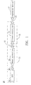
- FIG. 1 is a diagram of a portable electronic device according to the preferred embodiment of the invention.
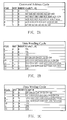
- FIG. 2A shows the content of the command address cycle of the multi-function high speed bus.
- FIG. 2B shows the content of the data reading cycle of the multi-function high speed bus.
- FIG. 2C shows the content of the data writing cycle of the multi-function high speed bus.
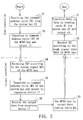
- FIG. 3 is the flow chart for the reading cycle when the multi-function high speed bus is used.
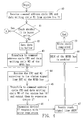
- FIG. 4 is the flow chart for the write cycle when the multi-function high speed bus is used.
- FIG. 5 is the flow chart of the burst write cycle when the multi-function high speed bus is used.
- FIG. 1 is a diagram of a portable electronic device according to the preferred embodiment of the invention.
- the portable electronic device 10 includes an electronic apparatus 11, an expansion pack 15, and an expansion device 17.
- the electronic apparatus 11 is, for example, a personal digital assistant (PDA).
- PDA personal digital assistant
- the expansion device is, for example, a memory card, a data card, or a network card.
- the expansion pack 15 can be detached in order to reduce the size and the weight.
- the interface between the electronic apparatus 11 and the expansion pack 15 is a multi-function high speed (MFHS) bus 12.
- MFHS multi-function high speed
- the expansion pack 15 is eclectically connected to the expansion device 17 by a system bus interface 14, such as the VLIO interface or the PCMCIA/CF interface.
- the expansion pack 15 is compatible with existing expansion devices.
- the electronic apparatus 11 includes a central process unit (CPU) 21, a system bus 22, and a host controller 23.
- the CPU 21 connects to the host controller 23 through the system bus 22.
- the host controller 23 bridges the signals between the system bus 22 and the MFHS bus 12 for communicating between the CPU 21 and the expansion pack 15.
- the expansion pack 15 includes a client controller 25.
- the client controller 25 transmits signals of the MFHS bus 12 to signals of the system bus 14, or transmits the signals of the system bus 14 to the signals of the MFHS bus 12.
- the CPU 21 communicates with the expansion device 17 through the host controller 23 and the client controller 25.
- the system buses 14 and 22 are the same standard, for example the VLIO or the PCMCIA/CF.
- the MFHS bus 12 includes a clock signal line CLK, a status signal line BST, a ready signal line BRDY, and 8 content signal lines CAD[7..0].
- the content signal lines CAD[7..0] transmit control signals, address signals and data signals.
- the CPU 21 transfers read cycles or write cycles to perform read or write on the expansion device 17.
- a read cycle includes a command address cycle and a data reading cycle;
- a write cycle includes a command address cycle and a data writing cycle.
- the host controller 23 transfers the command address cycle, and then transfers the data writing cycle; the write cycle is completed after the expansion device 17 confirms that the data is written successfully.
- the host controller 23 transfers a command address cycle; the read cycle is completed after the expansion device sends the requested data.
- Different buses are used to transmit the signals for the read/write cycles mentioned above by different methods due to the different number of transmission lines.
- the command address cycle includes a control signal and an address signal.
- the control signal includes at least an access mode signal, and a byte-enabling signal.
- the access mode signal represents whether this operation is read or write.
- the byte-enabling signal is used to control the number of byte of current read/write cycle, and it could be, for example, a byte, a word, a tri-byte, or a double-word.
- a data reading cycle includes a data signal that is the data sent by the expansion device 17 in reply of the requested from the command address cycle.
- the data writing cycle includes a data signal which is written in the expansion device 17 by the CPU 21.
- the existing VLIO bus or the PCMCIA/CF bus includes more transmission lines to transmit the control signal, the address signal, and the data signal.
- the control signal and the address signal of one command address signal is transmitted in one clock cycle.
- the number of pins is reduced according to the invention and one command address cycle is completed in a plurality of clock cycles.
- the data reading cycle and the data writing cycle is transferred in one clock cycle with for example a 24-bit data which would require a plurality of clock cycles for the data reading cycle and data writing cycle of the invention to complete.
- FIG. 2A shows the content of the command address cycle of the MFHS bus.
- the command address cycle uses 5 clock cycles for transmitting the control signal and the address signal.
- the transmission is not started, and the content signal lines CAD[7..0] are tri-stated (TS).
- the content signal lines CAD[7..0] are general command signals M[7..0] which are the command signal.
- the content signal lines CAD[7..0] are byte-enabling signals BE[3..0], reserve signals RS[1..0], and address signals A[25..24].
- the content signals lines CAD[7..0] are address signals A[23..16].
- the content signal lines CAD[7..0] are address signals A[15..8].
- the content signal lines CAD[7..0] are address signals A[7..0]. This command address cycle is used within a write cycle and a read cycle.
- FIG. 2B shows the content of the data reading cycle of the MFHS bus.
- the client controller 25 transforms the command address cycle and outputs the command address cycle to the expansion device 17.
- the expansion device 17 then returns the requested data to the client controller 25.
- the client controller 25 outputs the data reading cycle from the received data by the standard of the MFHS bus.
- the client controller 25 outputs the data reading cycle and enables the ready signal to acknowledge the host controller 23 that the data in the transmission lines are received.
- the duration between the host controller transferring the command address cycle and the host controller 23 receiving the data from the client controller 25 depends on the expansion device 17. For example, it is 3 clock cycles (clock cycle 6, 7, and 8) in this embodiment.
- the content signal lines CAD[7..0] are data signals D[7..0].
- the content signal lines CAD[7..0] are data signals D[15..8].
- the content signal lines CAD[7..0] are data signals D[23..16].
- the content signal lines CAD[7..0] are data signals D[31..24].
- the transmission of data D is completed and the ready signal line (BRDY) is disabled, the content signal lines CAD[7..0] are tri-stated (TS).
- FIG. 2C shows the content of the data writing cycle of the MFHS bus.
- the content signal lines CAD[7..0] are data signals D[7..0].
- the content signal lines CAD[7..0] are data signals D[15..8].
- the content signal lines CAD[7..0] are data signals D[23..16].
- the content signal lines CAD[7..0] are data signals D[31..24].
- the duration of the waiting is, for example, 2 clock cycles, clock cycles 10 and 11.
- the expansion device 17 confirms the writing is complete, the expansion device 17 transfers a response to the client controller 25.
- the client controller 25 enables the ready signal line BRDY of the MFHS bus at clock cycle 12 in order to acknowledge the host controller 23 that the data writing cycle is completed.
- FIG. 3 is the flow chart for the reading cycle when the MFHS bus is used.
- the host controller 23 receives a command address cycle CR1 from the CPU through the system bus 22.
- the host controller 23 transforms the command address cycle CR1 into a command address cycle CR2 of the MFSH bus and outputs to the client controller 25 (step 33).
- the client controller 25 acknowledged by an enabled ready signal line BST, starts to receive a command address cycle CR2 (step 34).
- the client controller 25 transforms the command address cycle CR2 into a command address cycle CR3 of the system bus 14 and outputs the command address cycle CR3 to the expansion device 17 (step 36).
- the client controller 25 receives the data from the expansion device 17 according to the command address cycle CR3 (step 38).
- the client controller 25 outputs the received data in a data reading cycle R2 of the MFHS bus (step 39).
- the ready signal line BRDY is then enabled.
- the host controller 23 receives the data according to the enabled ready signal line BRDY of the MFHS bus. Following that, the host controller 23 outputs the received data in the data reading cycle R1 to the CPU 21 (step 37), and completes the read cycle.
- the host controller 23 transfers a pause command to the CPU 21 in order to prevent any read cycle or write cycle being transferred before current read cycle is completed. After the host controller 23 confirms that the requested data is received, the pause command is abandoned.
- FIG. 4 is the flow chart for the write cycle when the MFHS bus is used.
- the host controller 23 receives a command address cycle CW1 and a data writing cycle W1 of the writing cycle sent by the CPU 21 through the system bus 22 (step 40).
- the host controller 23 checks whether the command address cycle CW1 is a burst write (step 41). If the command address cycle CW1 is a burst write, then the following step is node A, otherwise the following step is 42.
- step 42 the host controller 23 saves the data of the data writing cycle W1 into a buffer.
- the host controller 23 transforms both the command address cycle CW1 and the data writing cycle W1 into a command address cycle CW2 and a data writing cycle W2 of the MFHS bus respectively and outputs the command address cycle CW2 and the data writing cycle W2 (step 43).
- the client controller 25 receives the command address cycle CW2 and the data writing cycle W2 according to the enabled status signal line of the MFHS bus (step 44). After that, the client controller 25 transforms the command address cycle CW2 and the data writing cycle W2 into a command address cycle CW3 and a data writing cycle W3 of the system bus respectively, and outputs the command address cycle CW3 and the data writing cycle W3 to the expansion device 17 (step 45).
- the client controller 25 receives the response signal after the expansion device 17 completes writing status(step 46), and then the ready signal line BRDY of the MFHS bus is enabled (step 47). After the host controller 23 detects that the ready signal line BRDY is enabled (step 48), the write cycle is completed (step 49).
- step 42 the host controller 23 transmits a pause signal to the CPU 21 in order to prevent another read or write cycle being transferred until the host controller 23 detects that the ready signal line BRDY is enabled.
- FIG. 5 is the flow chart of the burst write cycle when the MFHS bus is used.
- burst write in one time, writes data in 4 batches and requires 4 transmissions for the MFHS bus of the invention.
- the host controller 23 decides the write address (step 50).
- the host controller 23 increases the write address each time until the burst write is completed.
- the data to be written is saved to the buffer (step 51).
- the host controller 23 then outputs the command address cycle CW2 and the data writing cycle W2 of the MFHS bus to the client controller 25 (step 52).
- the client controller 25 receives the command address cycle CW2 and the data writing cycle W2 according to the enabled status signal line BST of the MFHS bus(step 53).
- the client controller 25 transforms the command address cycle CW2 and the data writing cycle W2 into the command address cycle CW3 and data writing cycle W3 of system bus 14 and then outputs the command address cycle CW3 and data writing cycle W3 to the expansion device 17. After a period of waiting time, the client controller 25 receives a response signal for completing the write status from the expansion device 17 (step 55).
- the client controller 25 enables the ready signal line BRDY of the MFHS bus (step 56).
- the host controller 23 detects that the ready signal line BRDY is enabled (step 57). The host controller 23 then checks whether the burst write is completed. If the burst write is completed, the burst write cycle is completed otherwise the method returns to step 50, increases the write address, and continues the execution of the write cycle.
- the host controller 23 After the host controller 23 completes step 51, the host controller 23 transmits a pause signal to the CPU 21 in order to prevent another write or read cycle being transferred until the burst write cycle is completed.
- the embodiment of the portable electronic device mentioned above includes at least the following advantages:
Landscapes
- Engineering & Computer Science (AREA)
- General Engineering & Computer Science (AREA)
- Theoretical Computer Science (AREA)
- Computer Hardware Design (AREA)
- Physics & Mathematics (AREA)
- General Physics & Mathematics (AREA)
- Information Transfer Systems (AREA)
Abstract
Description
- The number of pins in the MFHS bus of the portable electronic device is less, therefore the size of the connector can be reduced resulting a smaller expansion pack which fits well with the trend for portable electronic devices to go smaller and lighter.
- The portable electronic device is compatible to and therefore can be used with existing expansion devices.
Claims (28)
- A main electronic apparatus of a portable electronic device for connecting to an expansion pack, the main electronic apparatus comprising:wherein the host controller bridges the signals on the P signal lines of the first system bus and the Q signal lines of the MFHS bus;a central processing unit (CPU);a first system bus, which is electrically connected to the CPU and includes P signal lines, where P is a positive integer;a multi-function high speed (MFHS) bus with Q signal lines, where Q is a positive integer and Q<P; anda host controller for communicating with the CPU through the first system bus and communicating with the expansion pack through the MFHS bus;
wherein the host controller transfers M clock signals of the first system bus to the MFHS bus in N clock cycles, where N is a positive integer and N>M. - The main electronic apparatus according to claim 1, wherein the signal lines of the MFHS bus comprises a clock signal line, a status signal line, a ready signal line, and a plurality of content signal lines; the number of the content signal lines are 8; and the content signal lines transmit a control signal, an address signal and a data signal.
- The main electronic apparatus according to claim 1, wherein the signal lines of the MFHS bus comprises a clock signal line, a status signal line, a ready signal line, and a plurality of content signal lines; the expansion pack includes a client controller which is connected to the MFHS bus and the expansion pack is connected to an expansion device for expanding function of the portable electronic device; the host controller enables the status signal line of the MFHS bus when the host controller transfers a command address cycle to the client controller; the command address cycle includes a control signal and an address signal; the control signal includes at least a byte-enabling mode and an access mode; and the access mode is a write mode or a read mode.
- The main electronic apparatus according to claim 1, wherein the signal lines of the MFHS bus comprises a clock signal line, a status signal line, a ready signal line, and a plurality of content signal lines; the expansion pack includes a client controller which is connected to the MFHS bus; the host controller enables the status signal line of the MFHS bus when the host controller transfers a command address cycle to the client controller; and when the access mode of the control signal of the command address cycle is a read mode, the client controller transfers a data writing cycle to the host controller according to the data output from the expansion device and the ready signal line is enabled.
- The main electronic apparatus according to claim 1, wherein the signal lines of the MFHS bus comprises a clock signal line, a status signal line, a ready signal line, and a plurality of content signal lines; the expansion pack includes a client controller which is connected to the MFHS bus; the host controller enables the status signal line of the MFHS bus when the host controller transfers a command address cycle to the client controller; the command address cycle includes a control signal and an address signal; and when the access mode of the control signal is a write mode, the client controller enables the ready signal line according to the expansion device in order to indicate the write mode is completed.
- The main electronic apparatus according to claim 1, wherein the signal lines of the MFHS bus comprises a clock signal line, a status signal line, a ready signal line, and a plurality of content signal lines; the expansion pack includes a client controller which is connected to the MFHS bus and the expansion pack is connected to an expansion device for expanding function of the portable electronic device; and the client controller communicates with the expansion device through a second system bus which includes R signal lines, where R is a positive integer and R>Q.
- The main electronic apparatus according to claim 6, wherein the client controller bridges the signals from the R signal lines of the second system bus and the signals from the Q signal lines of the MFHS bus.
- The main electronic apparatus according to claim 6, wherein the first system bus and second system bus are the same standard.
- An expansion pack of a portable electronic system, wherein the expansion pack is connected to a main electronic apparatus through an MFHS bus and is connected to an expansion device, the expansion pack comprising:wherein the MFHS bus includes Q signal lines and the Q signals further includes a clock signal line, a ready signal line, and a plurality of content signal line, where Q is a positive integer.a client controller, which is connected to the MFHS bus, for receiving a command address cycle from the main electronic apparatus and communicating with the expansion device according to the command address cycle,
- The expansion pack according to claim 9, wherein the number of the content signal line is 8 and the content signal lines transmit a control signal, an address signal and a data signal.
- The expansion pack according to claim 9, wherein the main electronic apparatus comprises:wherein the host controller bridges the signals on the P signal lines of the first system bus and the Q signal lines of the MFHS bus.a CPU;a first system bus, which is electrically connected to the CPU and includes P signal lines, where P is a positive integer and P>Q; anda host controller for communicating with the CPU through the first system bus and communicating with the expansion pack through the MFHS bus;
- The portable electronic device according to claim 11, wherein the host controller enables the status signal line of the MFHS bus when the host controller transfers a command address cycle to the client controller; the command address cycle transmits a control signal and an address signal; the control signal includes at least a byte-enabling mode and an access mode; and the access mode is a write mode or a read mode.
- The portable electronic device according to claim 12, wherein when the access mode is a read mode, the client controller transfers a data reading cycle to the host controller according to the expansion device and the ready signal line is enabled.
- The portable electronic device according to claim 12, wherein when the access mode is a write mode, the client controller enables the ready signal line according to the expansion device in order to indicate the write mode is completed.
- A reading method of a portable electronic system with an MFHS bus, the portable electronic system including a main electronic apparatus, an expansion pack, and an expansion device, wherein the main electronic apparatus is connected to the expansion pack by the MFHS bus; the main electronic apparatus includes a CPU and a host controller which is connected to the CPU by a first system bus; the expansion pack includes a client controller which is connected to the host controller by the MFHS bus and is connected to the expansion device by a second system bus; and the MFHS bus includes a clock signal line, a status line, a ready signal line, and a plurality of content signal line, the reading method comprising:outputting a first command address cycle from the CPU to the first system bus;receiving the first command address cycle which is outputted from the first system bus in M clock cycles by the host controller;transforming the first command address cycle into a second command address cycle by the host controller and transferring the second command address cycle through the MFHS bus in N clock cycle, thereby enabling the status signal line of the MFHS bus, where N>M;receiving the second command address cycle by the client controller when the status signal line is enabled;transforming the second command address cycle into a third command address cycle by the client controller and transferring a third command address cycle through first set of P client signal lines in K clock cycles, where K is a positive integer; andtransferring the third command address cycle to the expansion device by the second system bus.
- The reading method according to claim 15, wherein the first command address cycle includes a control signal and an address signal; and the access mode of the control signal is a read mode.
- The reading method according to claim 15, wherein when the host controller receives the first command address cycle, the host controller transmits a pause signal to the CPU.
- The reading method according to claim 15 further comprising:outputting a data to the second system bus according to the third command address cycle by the expansion device;receiving the data and transforming the data into a first data reading cycle by the client controller;transferring the first data reading cycle by the MFHS bus, whereby the ready signal line of the MFHS bus is enabled;receiving the first data reading cycle according to the enabled ready-signal line of the MFHS bus by the host controller;transforming the first data reading cycle into a second data reading cycle by the host controller; andtransferring the second data reading cycle to the CPU by the first system bus.
- The reading method according to claim 15, wherein when the host controller receives the first data reading cycle, the host controller enables the CPU.
- Awriting method of a portable electronic system with an MFHS bus, the portable electronic system including a main electronic apparatus, an expansion pack, and an expansion device, wherein the main electronic apparatus is connected to the expansion pack by the MFHS bus; the main electronic apparatus includes a CPU and a host controller which is connected to the CPU by a first system bus; the expansion pack includes a client controller which is connected to the host controller by the MFHS bus and is connected to the expansion device by a second system bus; and the MFHS bus includes a clock signal line, a status line, a ready signal line, and a plurality of content signal line, the writing method comprising:outputting a first command address cycle and a first data writing cycle from the CPU to the first system bus;receiving the first command address cycle and the first writing cycle in M clock cycles by the host controller, where M is a positive integer;transforming the first command address cycle into a second command address cycle, transforming the first data writing cycle into a second data writing cycle by the host controller, and transferring the second command address cycle and the second data writing cycle to the MFHS bus in N clock cycles, where N is a positive integer and N>M;receiving the second command address cycle and the second data writing cycle by the client controller when the status signal line is enabled; andtransforming the second command address cycle into a third command address cycle, transforming the second data writing cycle to a third data writing cycle by the client controller, and transferring the third command address cycle and the third data writing cycle through the second system bus in K clock cycles, where K is a positive integer.
- The writing method according to claim 20 further comprising:writing the data of the third data writing cycle according to the third command address cycle by the expansion device, and responding a write completion signal to the client controller; andenabling the ready signal line of the MFHS bus according to the write completion signal by the client controller.
- The writing method according to claim 21 further comprising:transferring a write cycle completion signal to the CPU according to the enabled ready signal line by the host controller.
- The writing method according to claim 21, wherein when the host controller receives the first command address cycle and the first data writing cycle, the host controller transmits a pause signal to the CPU.
- The method according to claim 23, wherein the host controller enables the CPU after the ready signal line is enabled.
- The method according to claim 22, wherein when the host controller receives the first command address cycle and the first data writing cycle, the host controller checks whether the first command cycle and the first data writing cycle is for a burst write; and if the first command cycle and the first data writing cycle is for a burst write, the writing method is repeated to write the data of the burst write into the expansion device.
- A writing method of a portable electronic system with an MFHS bus, the portable electronic system including a main electronic apparatus, an expansion pack, and an expansion device, wherein the main electronic apparatus is connected to the expansion pack by the MFHS bus; the main electronic apparatus includes a CPU and a host controller which is connected to the CPU by a first system bus; the expansion pack includes a client controller which is connected to the host controller by the MFHS bus and is connected to the expansion device by a second system bus; and the MFHS bus includes a clock signal line, a status line, a ready signal line, and a plurality of content signal line, the writing method comprising:outputting a first command address cycle and a first data writing cycle from the CPU to the first system bus, wherein the first command address cycle is a burst write cycle;receiving the first command address cycle and the first data writing cycle which are outputted from the first system bus in M clock cycles by the host controller, where M is a positive integer;deciding a write address by the host controller;transforming the first command address cycle into a second command address cycle according to the write address and transforming the first data writing cycle into a second data writing cycle by the host controller, and outputting the second command address cycle and the second data writing cycle through the MFHS bus in N clock cycles, where N is a positive integer and N>M;receiving the second command address cycle and the second data writing cycle by the client controller when the status signal line is enabled;transforming the second command address cycle into a third command address cycle, transforming the second data writing cycle into a third data writing cycle by the client controller, and transferring the third command address cycle and the third data writing cycle through the second system bus in K clock cycles, where K is a positive integer;writing the data of the third data writing cycle according to the third command address cycle by the expansion device, and responding a write completion signal to the client controller;enabling the ready signal line of the MFHS bus according to the write completion signal by the client controller; anddetermining whether the burst write cycle is completed by checking the enabled ready signal line by the host controller; and if the burst write cycle being not completed, returning to the step of deciding the write address; if the burst write cycle being completed, the host controller transferring a write cycle completion signal to the CPU.
- The writing method according to claim 26, wherein when the host controller receives the first command address cycle and the first data writing cycle, the host controller transmits a pause signal to the CPU.
- The writing method according to claim 27, wherein the host controller enables the CPU after the burst write is completed.
Priority Applications (2)
| Application Number | Priority Date | Filing Date | Title |
|---|---|---|---|
| EP20040013012 EP1603050B8 (en) | 2004-06-02 | 2004-06-02 | Portable electronic system and accessing method thereof |
| DE200460017285 DE602004017285D1 (en) | 2004-06-02 | 2004-06-02 | Portable electronic system and corresponding access method |
Applications Claiming Priority (1)
| Application Number | Priority Date | Filing Date | Title |
|---|---|---|---|
| EP20040013012 EP1603050B8 (en) | 2004-06-02 | 2004-06-02 | Portable electronic system and accessing method thereof |
Publications (3)
| Publication Number | Publication Date |
|---|---|
| EP1603050A1 true EP1603050A1 (en) | 2005-12-07 |
| EP1603050B1 EP1603050B1 (en) | 2008-10-22 |
| EP1603050B8 EP1603050B8 (en) | 2009-03-18 |
Family
ID=34925215
Family Applications (1)
| Application Number | Title | Priority Date | Filing Date |
|---|---|---|---|
| EP20040013012 Expired - Lifetime EP1603050B8 (en) | 2004-06-02 | 2004-06-02 | Portable electronic system and accessing method thereof |
Country Status (2)
| Country | Link |
|---|---|
| EP (1) | EP1603050B8 (en) |
| DE (1) | DE602004017285D1 (en) |
Citations (4)
| Publication number | Priority date | Publication date | Assignee | Title |
|---|---|---|---|---|
| US5761443A (en) * | 1995-06-07 | 1998-06-02 | Advanced Micro Systems, Inc. | Computer system employing a bus conversion bridge for interfacing a master device residing on a multiplexed peripheral bus to a slave device residing on a split-address, split-data multiplexed peripheral bus |
| US5781748A (en) * | 1996-07-19 | 1998-07-14 | Compaq Computer Corporation | Computer system utilizing two ISA busses coupled to a mezzanine bus |
| US5826048A (en) * | 1997-01-31 | 1998-10-20 | Vlsi Technology, Inc. | PCI bus with reduced number of signals |
| US6212590B1 (en) * | 1997-12-22 | 2001-04-03 | Compaq Computer Corporation | Computer system having integrated bus bridge design with delayed transaction arbitration mechanism employed within laptop computer docked to expansion base |
-
2004
- 2004-06-02 EP EP20040013012 patent/EP1603050B8/en not_active Expired - Lifetime
- 2004-06-02 DE DE200460017285 patent/DE602004017285D1/en not_active Expired - Lifetime
Patent Citations (4)
| Publication number | Priority date | Publication date | Assignee | Title |
|---|---|---|---|---|
| US5761443A (en) * | 1995-06-07 | 1998-06-02 | Advanced Micro Systems, Inc. | Computer system employing a bus conversion bridge for interfacing a master device residing on a multiplexed peripheral bus to a slave device residing on a split-address, split-data multiplexed peripheral bus |
| US5781748A (en) * | 1996-07-19 | 1998-07-14 | Compaq Computer Corporation | Computer system utilizing two ISA busses coupled to a mezzanine bus |
| US5826048A (en) * | 1997-01-31 | 1998-10-20 | Vlsi Technology, Inc. | PCI bus with reduced number of signals |
| US6212590B1 (en) * | 1997-12-22 | 2001-04-03 | Compaq Computer Corporation | Computer system having integrated bus bridge design with delayed transaction arbitration mechanism employed within laptop computer docked to expansion base |
Also Published As
| Publication number | Publication date |
|---|---|
| EP1603050B8 (en) | 2009-03-18 |
| EP1603050B1 (en) | 2008-10-22 |
| DE602004017285D1 (en) | 2008-12-04 |
Similar Documents
| Publication | Publication Date | Title |
|---|---|---|
| JP4649009B2 (en) | Information processing apparatus having a card interface, card-type electronic equipment that can be mounted on the apparatus, and operation mode setting method in the apparatus | |
| KR101988260B1 (en) | EMBEDDED MULTIMEDIA CARD(eMMC), AND METHOD FOR OPERATING THE eMMC | |
| CN107908589B (en) | I3C communication verification system and method for verifying slave device and master-slave device | |
| US7660938B1 (en) | Flash card reader and data exchanger utilizing low power extended USB protocol without polling | |
| JP4799417B2 (en) | Host controller | |
| US5564114A (en) | Method and an arrangement for handshaking on a bus to transfer information between devices in a computer system | |
| EP2040174A1 (en) | Card-type peripheral device | |
| US10725949B2 (en) | Slave-to-slave direct communication | |
| WO2007118107A2 (en) | Wireless flash memory card expansion system | |
| KR100240922B1 (en) | Method for slave dma emulation on a computer system bus | |
| US9680972B2 (en) | SD switch box in a cellular handset | |
| KR100440972B1 (en) | Apparatus and method for establishing data transfer mode by card insertion identification | |
| US7102671B1 (en) | Enhanced compact flash memory card | |
| CN101496379B (en) | Non-volatile storage device with USB and wireless connection and method of controlling the connection | |
| US8527667B2 (en) | Apparatuses and methods for transferring data | |
| US7469304B2 (en) | Data transfer control device, electronic equipment, and method for a data transfer through a bus, the data transfer control device including a register and a packet buffer that are commonly used during a host operation and a peripheral operation | |
| CN103885910B (en) | Method for IIC communication between multiple devices in master mode | |
| WO2008085240A1 (en) | Universal serial bus host controller | |
| US7162562B2 (en) | Portable electronic system and accessing method thereof | |
| JP4037788B2 (en) | Signal transmission device between control chipsets | |
| CN118277319B (en) | Data transmission control method and device based on LPC bus and electronic equipment | |
| EP1603050B1 (en) | Portable electronic system and accessing method thereof | |
| MX2007005812A (en) | Multimedia card interface method, computer program product and apparatus. | |
| CN100451668C (en) | Storage bus check procedure | |
| CN116601620B (en) | Message notification method and device |
Legal Events
| Date | Code | Title | Description |
|---|---|---|---|
| PUAI | Public reference made under article 153(3) epc to a published international application that has entered the european phase |
Free format text: ORIGINAL CODE: 0009012 |
|
| AK | Designated contracting states |
Kind code of ref document: A1 Designated state(s): AT BE BG CH CY CZ DE DK EE ES FI FR GB GR HU IE IT LI LU MC NL PL PT RO SE SI SK TR |
|
| AX | Request for extension of the european patent |
Extension state: AL HR LT LV MK |
|
| 17P | Request for examination filed |
Effective date: 20060322 |
|
| 17Q | First examination report despatched |
Effective date: 20060621 |
|
| AKX | Designation fees paid |
Designated state(s): DE FR GB |
|
| GRAP | Despatch of communication of intention to grant a patent |
Free format text: ORIGINAL CODE: EPIDOSNIGR1 |
|
| GRAS | Grant fee paid |
Free format text: ORIGINAL CODE: EPIDOSNIGR3 |
|
| GRAA | (expected) grant |
Free format text: ORIGINAL CODE: 0009210 |
|
| RIN1 | Information on inventor provided before grant (corrected) |
Inventor name: LEE, CHI-FENG Inventor name: KUAN, TSUNG-PAO Inventor name: CHEN, REN-PENG Inventor name: LIU, WAN-HSIEH Inventor name: HSU, SHIH-MING |
|
| AK | Designated contracting states |
Kind code of ref document: B1 Designated state(s): DE FR GB |
|
| REG | Reference to a national code |
Ref country code: GB Ref legal event code: FG4D |
|
| REF | Corresponds to: |
Ref document number: 602004017285 Country of ref document: DE Date of ref document: 20081204 Kind code of ref document: P |
|
| RAP2 | Party data changed (patent owner data changed or rights of a patent transferred) |
Owner name: HTC CORPORATION |
|
| PLBE | No opposition filed within time limit |
Free format text: ORIGINAL CODE: 0009261 |
|
| STAA | Information on the status of an ep patent application or granted ep patent |
Free format text: STATUS: NO OPPOSITION FILED WITHIN TIME LIMIT |
|
| 26N | No opposition filed |
Effective date: 20090723 |
|
| REG | Reference to a national code |
Ref country code: FR Ref legal event code: PLFP Year of fee payment: 13 |
|
| REG | Reference to a national code |
Ref country code: FR Ref legal event code: PLFP Year of fee payment: 14 |
|
| REG | Reference to a national code |
Ref country code: FR Ref legal event code: PLFP Year of fee payment: 15 |
|
| REG | Reference to a national code |
Ref country code: FR Ref legal event code: PLFP Year of fee payment: 20 |
|
| P01 | Opt-out of the competence of the unified patent court (upc) registered |
Effective date: 20230602 |
|
| PGFP | Annual fee paid to national office [announced via postgrant information from national office to epo] |
Ref country code: FR Payment date: 20230411 Year of fee payment: 20 Ref country code: DE Payment date: 20230404 Year of fee payment: 20 |
|
| PGFP | Annual fee paid to national office [announced via postgrant information from national office to epo] |
Ref country code: GB Payment date: 20230413 Year of fee payment: 20 |
|
| REG | Reference to a national code |
Ref country code: DE Ref legal event code: R071 Ref document number: 602004017285 Country of ref document: DE |
|
| REG | Reference to a national code |
Ref country code: GB Ref legal event code: PE20 Expiry date: 20240601 |
|
| PG25 | Lapsed in a contracting state [announced via postgrant information from national office to epo] |
Ref country code: GB Free format text: LAPSE BECAUSE OF EXPIRATION OF PROTECTION Effective date: 20240601 |
|
| PG25 | Lapsed in a contracting state [announced via postgrant information from national office to epo] |
Ref country code: GB Free format text: LAPSE BECAUSE OF EXPIRATION OF PROTECTION Effective date: 20240601 |