EP1602983A1 - Water soluble resin composition, method of pattern formation and method of inspecting resist pattern - Google Patents
Water soluble resin composition, method of pattern formation and method of inspecting resist pattern Download PDFInfo
- Publication number
- EP1602983A1 EP1602983A1 EP04711490A EP04711490A EP1602983A1 EP 1602983 A1 EP1602983 A1 EP 1602983A1 EP 04711490 A EP04711490 A EP 04711490A EP 04711490 A EP04711490 A EP 04711490A EP 1602983 A1 EP1602983 A1 EP 1602983A1
- Authority
- EP
- European Patent Office
- Prior art keywords
- resist pattern
- water
- resin composition
- soluble resin
- described before
- Prior art date
- Legal status (The legal status is an assumption and is not a legal conclusion. Google has not performed a legal analysis and makes no representation as to the accuracy of the status listed.)
- Granted
Links
- 0 C*(C)C(*)(CN)N(CCC1)C1=O Chemical compound C*(C)C(*)(CN)N(CCC1)C1=O 0.000 description 2
- MCTWTZJPVLRJOU-UHFFFAOYSA-N C[n]1cncc1 Chemical compound C[n]1cncc1 MCTWTZJPVLRJOU-UHFFFAOYSA-N 0.000 description 1
Images


Classifications
-
- G—PHYSICS
- G03—PHOTOGRAPHY; CINEMATOGRAPHY; ANALOGOUS TECHNIQUES USING WAVES OTHER THAN OPTICAL WAVES; ELECTROGRAPHY; HOLOGRAPHY
- G03F—PHOTOMECHANICAL PRODUCTION OF TEXTURED OR PATTERNED SURFACES, e.g. FOR PRINTING, FOR PROCESSING OF SEMICONDUCTOR DEVICES; MATERIALS THEREFOR; ORIGINALS THEREFOR; APPARATUS SPECIALLY ADAPTED THEREFOR
- G03F7/00—Photomechanical, e.g. photolithographic, production of textured or patterned surfaces, e.g. printing surfaces; Materials therefor, e.g. comprising photoresists; Apparatus specially adapted therefor
- G03F7/26—Processing photosensitive materials; Apparatus therefor
- G03F7/40—Treatment after imagewise removal, e.g. baking
-
- C—CHEMISTRY; METALLURGY
- C08—ORGANIC MACROMOLECULAR COMPOUNDS; THEIR PREPARATION OR CHEMICAL WORKING-UP; COMPOSITIONS BASED THEREON
- C08L—COMPOSITIONS OF MACROMOLECULAR COMPOUNDS
- C08L39/00—Compositions of homopolymers or copolymers of compounds having one or more unsaturated aliphatic radicals, each having only one carbon-to-carbon double bond, and at least one being terminated by a single or double bond to nitrogen or by a heterocyclic ring containing nitrogen; Compositions of derivatives of such polymers
-
- Y—GENERAL TAGGING OF NEW TECHNOLOGICAL DEVELOPMENTS; GENERAL TAGGING OF CROSS-SECTIONAL TECHNOLOGIES SPANNING OVER SEVERAL SECTIONS OF THE IPC; TECHNICAL SUBJECTS COVERED BY FORMER USPC CROSS-REFERENCE ART COLLECTIONS [XRACs] AND DIGESTS
- Y10—TECHNICAL SUBJECTS COVERED BY FORMER USPC
- Y10S—TECHNICAL SUBJECTS COVERED BY FORMER USPC CROSS-REFERENCE ART COLLECTIONS [XRACs] AND DIGESTS
- Y10S430/00—Radiation imagery chemistry: process, composition, or product thereof
- Y10S430/1053—Imaging affecting physical property or radiation sensitive material, or producing nonplanar or printing surface - process, composition, or product: radiation sensitive composition or product or process of making binder containing
- Y10S430/1055—Radiation sensitive composition or product or process of making
- Y10S430/114—Initiator containing
- Y10S430/115—Cationic or anionic
-
- Y—GENERAL TAGGING OF NEW TECHNOLOGICAL DEVELOPMENTS; GENERAL TAGGING OF CROSS-SECTIONAL TECHNOLOGIES SPANNING OVER SEVERAL SECTIONS OF THE IPC; TECHNICAL SUBJECTS COVERED BY FORMER USPC CROSS-REFERENCE ART COLLECTIONS [XRACs] AND DIGESTS
- Y10—TECHNICAL SUBJECTS COVERED BY FORMER USPC
- Y10S—TECHNICAL SUBJECTS COVERED BY FORMER USPC CROSS-REFERENCE ART COLLECTIONS [XRACs] AND DIGESTS
- Y10S430/00—Radiation imagery chemistry: process, composition, or product thereof
- Y10S430/165—Thermal imaging composition
Definitions
- the present invention relates to a resist pattern forming method by which a separation size or a hole aperture size of the resist pattern is reduced practically and effectively below a limit resolution by forming a coated layer on a resist pattern by use of a water-soluble resin composition, then forming a modified layer which is insoluble in a developer on the surface of the resist pattern by modifying the coated layer adjoining the resist pattern, and thereby thickening the resist pattern upon formation of a resist pattern in a semiconductor manufacturing process; a method of reducing a dimensional fluctuation of a resist pattern that occurs upon electron beam irradiation of a size measuring SEM by said modified layer; an improved inspection method of a size measurement of a resist pattern using a size measuring SEM; and a water-soluble resin composition used for these methods favorably and suitably.
- photolithography technology In the various fields such as a manufacture of semiconductor device such like an LSI, a preparation of a flat panel display (FPD) such like a liquid crystal display (LCD) panel, a manufacture of a circuit substrate such like a thermal head and so on, photolithography technology has so far been employed for forming microelements or for conducting fine processing.
- a positive or negative-working photosensitive resin composition photoresist
- photoresist is used to form a resist pattern.
- the thus-formed resist patterns are put to use as an etching resist and a resist applied upon impurity ion implantation in manufacturing of, for example, a semiconductor device, an FPD and a circuit substrate or as a plating resist and so on in manufacturing of a magnetic head, and so on.
- a following fine pattern forming method has been proposed wherein a positive or negative-working photoresist so far publicly known is used as a photoresist. That is, after forming a resist pattern by the pattern forming method so far publicly known, an acid-crosslinkable material layer for forming a coated layer is formed on the thus-formed resist pattern. The material layer is then crosslinked and hardened utilizing diffusion of an acid from the resist pattern by heating to be made insoluble in a developer.
- Patent Literature 1 Japanese Laid-Open Patent Publication No. Hei 5-241,348
- Patent Literature 2 Japanese Laid-Open Patent Publication No. Hei 6-250,379
- Patent Literature 3 Japanese Laid-Open Patent Publication No. Hei 10-73,927
- the above-described method is being paid attention to be a useful method as it is not necessary to invest a high price facility such as light-exposure device for a short wavelength and is possible to cut down a dimension of a space area in a resist pattern practically and effectively.
- the above-described fine resist pattern forming method so far proposed wherein a fine resist pattern below a limit resolution of light-exposure wavelength is formed practically and effectively by thickening a resist pattern and narrowing thereby a width between a resist pattern and the other resist pattern, is mainly directed to a resist pattern formed by a KrF resist (KrF responsive radiation sensitive resin composition) and it exhibited the effect towards a KrF resist.
- a KrF resist KrF responsive radiation sensitive resin composition
- ArF resist ArF responsive radiation sensitive resin composition
- a polymer having a structure such that a protecting group is introduced into acrylic resin, methacrylic resin or the like is becoming a leading material naturally as the ArF resist.
- an alicyclic protecting group has been proposed, and a hydrophobic property of the polymer itself is getting higher by the introduction of the alicyclic protecting group.
- a composition for forming a coated layer is a composition comprising a water-soluble resin and water as main components in order not to dissolve a resist pattern film which constitutes the first layer.
- a water-soluble resin composition for forming a coated layer so far proposed is not regarded to have a good applying property on a resist pattern of high water repellency such an ArF resist described before.
- An object of the present invention is to propose a pattern forming method of reducing a separation size or a hole aperture size of a resist pattern below a limit resolution practically and effectively and in a high dimensional controllability, wherein a coated layer is applied on the resist pattern such as an ArF resist pattern which is formed by a way so far applied and has a relatively high water repellency and then modified by heating to form a modified layer which is insoluble in a developer on the surface of the resist pattern and thicken thereby the resist pattern.
- Another objects of the present invention are to propose a method of reducing a dimensional fluctuation of the resist pattern caused by an electron beam exposure after a pattern formation, wherein a coated layer is given on a resist pattern such as an ArF resist pattern which is formed by a way so far applied and has a relatively high water repellency and then a modified layer which is insoluble in a developer is formed on the surface of the resist pattern by modification of the coated layer by heating; and an inspection method of a resist pattern by which a dimensional fluctuation caused by irradiation of an electron beam is reduced upon above-described inspection of a size measurement for the resist pattern with a size measuring SEM.
- a coated layer such as an ArF resist pattern which is formed by a way so far applied and has a relatively high water repellency and then a modified layer which is insoluble in a developer is formed on the surface of the resist pattern by modification of the coated layer by heating
- Another object of the present invention is to propose a water-soluble resin composition which is preferably and suitably used for forming the coated layer in the above-described pattern forming method of reducing a separation size or a hole aperture size of the resist pattern practically and effectively below a limit resolution by thickening the resist pattern, the above-described method of reducing a dimensional fluctuation of is reduced.
- the present inventors found that the above-described various kind of objects can be attained by containing of an acid generator that can generate an acid by heating in the above-described water-soluble resin compositionwhich is a coated layer formingmaterial used for coating the resist pattern and further by making it possible to provide a resist pattern with a resistance to an electron beam when using a particular type of polymer as a water-soluble resin to reach to the present invention.
- the present invention relates to a water-soluble resin composition characterized in comprising at least a water-soluble resin, an acid generator that can generate an acid by heating and a solvent containing water.
- the present invention also relates to a pattern forming method to reduce a separation size or a hole aperture size of a resist pattern practically and effectively below a limit resolution, which is characterized in comprising a step of forming a coated layer by applying the water-soluble resin composition on a resist pattern, a step of forming a modified layer of the coated layer which is made insoluble in a developer in a determined width on a surface of the resist pattern described before by heating the coated layer described before, and a step of forming a pattern having the modified layer on a surface of the resist pattern by developing the coated layer described before.
- the present invention further relates to a method to reduce a dimensional fluctuation of a resist pattern caused by electron beam irradiation, which is characterized in comprising a step of forming a coated layer by applying the water-soluble resin composition described above on a resist pattern, a step of forming a modified layer of the coated layer which is made insoluble in a developer in a determined width on a surface of the resist pattern described before by heating the coated layer described before, and a step of forming a pattern having the modified layer on a surface of the resist pattern by developing the coated layer described before.
- the present invention further relates to an inspection method of a resist pattern, which is characterized in comprising a step of forming a coated layer by applying the water-soluble resin composition described above on a resist pattern, a step of forming a modified layer of the coated layer which is made insoluble in a developer in a determined width on a surface of the resist pattern described before by heating the coated layer described before, a step of forming a pattern having the modified layer on a surface of the resist pattern by developing the coated layer described before, and a step of measuring a resist pattern size by an electron beam irradiation to the pattern described before.
- the present invention will be further described in more detail on the water-soluble resin composition of the present invention and a pattern forming method using the water-soluble resin composition, a method to reduce the fluctuation of a size measurement value of a resist pattern by irradiation of an electron beam and an inspection method of a resist pattern.
- the water-soluble resin composition of the present invention comprises at least a water-soluble resin, an acid generator that can generate an acid by heating and a solvent containing water.
- a water-soluble resin used in the water-soluble resin composition of the present invention any water-soluble resin so far applied can be used if a solubility of the resin in water is 0.1 weight % or higher.
- the water-soluble resin used in the water-soluble resin composition of the present invention there can be exemplified a homopolymer or a multi-component copolymer of vinyl monomer with a hydrophilic group, and a polycondensated polymer with a hydrophilic group.
- these resins include polyvinyl alcohol (including a partially saponified substance), polyacrylic acid, polymethacrylic acid, poly(2-hydroxyethylacrylate),poly(2-hydroxyethylmethacrylate), poly(4-hydroxybutyl acrylate), poly(4-hydroxybutyl methacrylate), poly(glycosiloxyethyl acrylate), poly(glycosiloxyethyl methacrylate), polyvinylmethyl ether, polyvinylpyrrolidone, polyethylene glycol, polyvinyl acetal (including a partially acetalized substance), polyethyleneimine, polyethyleneoxide, a copolymer of styrene and maleic anhydride, polyvinylamine, polyallylamine, a water-soluble resin containing an oxazoline group, a water-soluble melamine resin, a water-soluble urea resin, alkyd resin, sulfonamide or salts thereof.
- a copolymer represented by the general formula described below is particularly favorable.
- This polymer may be either a random copolymer or a block copolymer, however a random copolymer is preferable.
- R 1 and R 2 each represent independently a hydrogen atom or a methyl group
- R 3 represents a hydroxyl group, a carboxyl group, -OCOR 4 or
- R 4 represents an alkyl group
- m and n each are a number of 10 to 100,000.
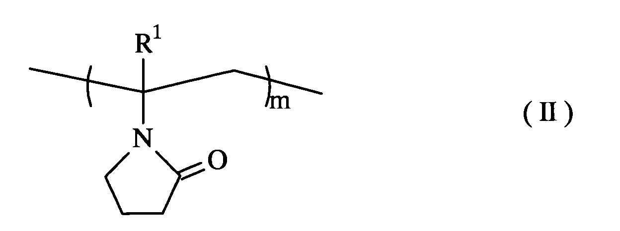
- a polymer represented by the general formula (II) described below is also a water-soluble resin which can be preferably applied.
- R 1 represents a hydrogen atom or a methyl group and m is a number of 10 to 100,000.
- the weight average molecular weight of the water-soluble resin is preferably 1,000 to 1,000,000, more preferably 3,000 to 200,000.
- the molecular weight of the resin is less than 1,000, the applicability thereof is deteriorated to be hardly able to obtain a film with a homogeneous quality and simultaneously to reduce a stability of an applied film with the elapse of time.
- the molecular weight is higher than 1,000,000, a stringy phenomenon is taken place upon the application or spreading on a resist surface becomes worse to be unable to obtain a homogeneous coated film by application with a small dropping amount.
- a permeability of a filter is inferior.
- the water-soluble resin composition of the present invention is applied for forming a protecting modified layer in order to control a size measurement fluctuation of a resist pattern caused by an electron beam upon measuring of a resist pattern size by SEM
- the water-soluble resin is preferably to be a particular type of polymer showing a determined level of resistance to electron beam irradiation to be generated by a size measuring SEM, for example a polymer having an imidazole group.
- an acid generator able to generate an acid by heating and used in the water-soluble resin composition of the present invention a compound generating an acid by heating at 70 to 160°C is preferred and an amine salt of an organic acid is preferred above all although there is no restriction if it may generate an acid by heating and it may be a water-soluble compound.
- an acid generator represented by the general formula described below is preferred. Wherein R 5 represents an alkyl group, a hydroxyl group or a carboxyl group.
- a surface active agent may be further added into the water-soluble resin composition of the present invention, if necessary.
- the surface active agent although there is no restriction if it may be able to improve an applicability of a water-soluble resin composition, there can be raised Fluorad manufactured by 3M company, Nonypol manufactured by Sanyo Kasei company, Megafac manufactured by Dai-Nippon Ink and Chemicals, Inc., acetylene alcohol such as a compound represented by the general formula (IV) described below for example, acethylene glycol, polyethoxylate of acethylene alcohol, polyethoxylate of acethylene glycol or the like.
- R 6 represents a linear or branched alkyl group having a carbon number of 1 to 20
- R 7 and R 8 each represent independently H or a linear or branched alkyl group having a carbon number of 1 to 3
- R 9 represents a linear or branched alkylene group having a carbon number of 1 to 20
- k is 0 or 1
- r and s each represent independently an integer including 0.
- acethylene alcohol, acethylene glycol, polyethoxylate of acethylene alcohol and polyethoxylate of acethylene glycol are particularly preferred.
- acetylene alcohol and acetylene glycol there are exemplified 3-methyl-1-butyne-3-ol, 3-methyl-1-pentyne-3-ol, 3,6-dimethyl-4-octyne-3,6-diol, 2,4,7,9-tetrametyl-5-decyne-4,7-diol, 3,5-dimethyl-1-hexyne-3-ol, 2,5-dimethy-3-hexyne-2,5-diol, 2,5-dimethyl-2,5-hexanediol and so on.
- polyethoxylate of acethylene alcohol and polyethoxylate of acethylene glycol there are exemplified polyethoxylate of acethylene alcohol or acethylene glycol which is concretely exemplified above.
- These surface active agents can be applied singly or in a mixture of two or more kinds thereof, the formulated amount thereof is preferably 50 to 2,000 ppm relative to a water-soluble resin composition, more preferably 100 to 1,000 ppm.
- the water which is used as a solvent in the water-soluble resin composition of the present invention is not particularly limited if it is water and one from which organic impurities or metal ions are removed by distillation, ion exchange treatment, filter treatment, a various kind of absorption treatments and so on is preferred.
- Water-soluble organic solvents are not limited if a solubility thereof in water is 0.1 weight % or higher.
- water-soluble organic solvents there can be exemplified alcohols such as methyl alcohol, ethyl alcohol, isopropyl alcohol and so on; ketones such as acetone, methylethylketone, 2-heptanone, cyclohexanone and so on; esters such as methyl acetate, ethyl acetate and so on; ethylene glycol monoalkyl ethers such as ethylene glycol monomethyl ether, ethylene glycol monoethyl ether and so on; ethylene glycol monoalkyl ether acetates such as ethylene glycol monomethyl ether acetate, ethylene glycol monoethyl ether acetate and so on; propylene glycol monoalkyl ethers such as propylene
- solvents lower alcohols having C 1 to C 4 such as methyl alcohol, ethyl alcohol, isopropyl alcohol and so on are preferable. These solvents can be used singly or in a mixture of two or more kinds thereof. These solvents can be used in the limit wherein a resist pattern is not solved out by a water-soluble resin composition which contains the solvent.
- water-soluble resin composition of the present invention it is preferred that 1 to 30 parts by weight of the water-soluble resin and 0.01 to 10 parts by weight of an acid generator relative to 100 parts by weight of the water-soluble resin composition are contained.
- a method to reduce a separation size or a hole aperture size of the resist pattern practically and effectively below a limit resolution by using the water-soluble resin composition of the present invention a method to reduce a size measurement fluctuation of a resist pattern caused by electron beam irradiation of size measuring SEM by using the water-soluble resin composition of the present invention, and an inspection method of a size measurement of a resist pattern by using a size measuring SEM are now explained by referring to diagrams if necessary.
- the case where a resist pattern is formed by an ArF resist will be raised as an example.
- the resist pattern according to each method of the present invention is not limited to the ArF resist pattern.
- Figures 1 (a) to 1 (e) show process diagrams to explain a method of forming a developer insoluble modified layer on a surface of an ArF resist pattern by using the water-soluble resin composition of the present invention and in each diagram, a substrate, a photoresist, a resist pattern, a coated layer, a modified layer and so on are shown as a cross section view showing a frame format.
- an ArF resist for example, a positive-working chemically amplified resist
- a substrate to be processed such as a semiconductor substrate 1, for example in order to form a photoresist layer 2 thereon.
- the photoresist layer 2 is exposed to light by using an irradiation device having an ArF excimer laser light source through a photo-mask which is not diagramed, followed by developing to form a positive-working pattern 3 (see Figure 1 (b)).
- a water-soluble resin composition of the present invention is applied as covering this resist layer 3 to form a coated layer 4.
- the resist pattern 3 and the coated layer 4 are heated.
- An acid generator which generates an acid by heating is contained in the water-soluble resin composition of the present invention, and the coated layer is chemicallymodified by an acid generated from the acid generator by heating.
- an area neighboring to the resist pattern 3 in the coated layer 4 is physically and chemically modified more intensively than other area to form a modified layer 5 which is made insoluble in a developer mentioned later.
- a chemical modification does not advance so much on other area of the coated layer, the area is kept in the soluble state in the developer (see Figure 1 (d)).
- the coated layer neighboring to the resist pattern 3 is more chemically modified than the other are is not clear, it is guessed to be one of the reasons that an intermixing between a surface area of the resist pattern 3 and the neighboring area to the resist pattern 3 in the coated layer 4 is taken place by heating, however the present invention being not limited by this reason.
- the coated layer 4 where the modified layer 5 which is made insoluble in the developer is developed to form a pattern having the modified layer 5 on a surface of the resist pattern 3 (see Figure 1 (e)).
- the modified layer 5 described above As described above, by forming the modified layer 5 described above on the surface (upper face and side face) of the resist pattern, the breadth between a resist pattern and a neighboring resist pattern is narrowed to make it possible to reduce a separation size or a hole aperture size of a resist pattern practically and effectively below a limit resolution.
- the modified layer described above can play a role of a protecting layer against an electron beam, it is possible to restrain a size measurement fluctuation of a resist pattern by irradiation of an electron beam of a size measuring SEM. Accordingly it is possible to restrain a dimensional fluctuation of a resist pattern as well as to conduct a size measurement of a resist pattern in a size measurement inspection of a resist pattern by a size measuring SEM.
- the radiation sensitive resin composition which is applicable to form the resist pattern 3 described above may be any radiation sensitive resin compositions so far publicly known and publicly applied.
- a radiation sensitive resin composition there can be raised a positive-working resist comprising an alkali-soluble resin such as novolak resin, a hydroxystyrene type resin or an acrylic resin and aquinone diazide compound, a chemically amplified positive or negative-working resist wherein an acid is generated by irradiation of light and a resist pattern is formed by a catalytic action of the generated acid, and so on.
- a chemically amplified positive-working resist wherein an acid is generated by irradiation of light and a resist pattern is formed by a catalytic action of the generated acid is preferred.
- the high water repellent resist pattern formed from, for example, an ArF resist it was so far difficult to form a crosslinked film of awater-soluble resin having sufficient film thickness on the resist pattern by forming a coating layer of a water-soluble resin to be crosslinked by an acid on the resist pattern and to crosslink the coating layer of the water-soluble resin by diffusion of an acid from the resist pattern.
- the radiation sensitive resin composition with a relatively highly water-repellant for example, ArF resist is preferred in the present invention.
- ArF resist it is known that a size measurement fluctuation of a resist pattern is taken place with the resist pattern formed by an ArF resist upon inspection by a size measuring SEM as already mentioned, and it is preferred that a radiation sensitive resin composition is an ArF resist from the view point to prevent it.
- ArF resists have been being proposed and come onto the market, any of those publicly known and publicly applied ArF resists can be used.
- a resist pattern forming method using a radiation sensitive resin composition may be any methods so far known including an application method, a light-exposure method, a baking method, a developing method, a rinsing method and so on.
- the radiation sensitive resin composition which is a coated layer forming material of the present invention there may be utilized a proper method such as a spin coating method, a spray coating method, a dipping application method, or a roller coating method which has so far been known. After being applied, the coated layer forming material is prebaked if necessary to make the coated layer 4.
- the conditions of heat treatment for the coated layer are a heating temperature of approximately 70 to 160°C and a heating time of approximately 60 to 120 seconds, preferably for 50 to 80 seconds.
- the heating temperature is preferably the temperature that an intermixing between a resist pattern and a coated layer is taken place.
- the film thickness of a modified layer to be formed can be adjusted properly by temperature and time of heat treatment, a radiation sensitive resin composition to be used, a water-soluble resin composition to be used, and so on. Therefore these conditions may be set up depending on how much it is necessary to thicken a resist pattern.
- the breadth (film thickness) of a modified layer is preferably made to be 2 to 100 nm.
- a developing agent that is applied for leaving the modified layer 5 which is formed by heating and removing unmodified coated layer
- water a mixed solution of water and a water-soluble organic solvent
- TMAH tetramethylammonium hydroxide
- Polyvinylpyrrolidone-co-polyvinylacetate 9.2 parts by weight triethylamine salt of paratoluene sulfonic acid 0.8 parts by weight and pure water 90.0 parts by weight were mixed and then stirred sufficiently to solve. Thereafter the solution was filtrated with a 0.2- ⁇ m filter to prepare a water-soluble resin composition A.
- Polyvinylpyrrolidone-co-polyvinylimidazole 4.5 parts by weight polyvinylpyrrolidone 0.8 parts by weight triethylamine salt of paratoluene sulfonic acid 0.9 parts by weight surfactant (Acetylenol EL manufactured by Kawaken Chemical company) 0.002 parts by weight and pure water 93.8 parts by weight were mixed and then stirred sufficiently to solve. Thereafter the solution was filtrated with a 0.2- ⁇ m filter to prepare a water-soluble resin composition B.
- a positive-working photosensitive resin composition AZ AX1050P-HS manufactured by Clariant Corporation ('AZ' is a trademark.) was applied on a silicon wafer of 6 inch in diameter treated with HMDS (hexamethyldisilazane) by a spin coater MK-8 manufactured by Tokyo Electron Co. , Limited and pre-baked at 115°C for 60 seconds on a hotplate to prepare a resist filmof approximately 0. 40 ⁇ m in thickness.
- HMDS hexamethyldisilazane
- the resist film was exposed to light through a pattern, in which hole patterns having various kind of diameter sizes exist, by use of a light-exposure device PAS5500/950 manufactured by ASML Company with an exposure wavelength of ArF excimer laser (193 nm) and a post-exposure-bake (PEB) was conducted at 110°C for 60 seconds on a hot plate. Thereafter the resist film was spray-paddle developed under the condition at 23°C for one minute using alkali developing agent AZ 300MIF Developer (a 2.38 % by weight an aqueous solution of tetramethylammonium hydroxide) manufactured by Clariant (Japan) K.K. to obtain a positive resist pattern.
- alkali developing agent AZ 300MIF Developer a 2.38 % by weight an aqueous solution of tetramethylammonium hydroxide manufactured by Clariant (Japan) K.K.
- the water-soluble resin composition A was applied on the thus-obtained hole pattern by a spin coater MK-8 manufactured by Tokyo Electron Co., Limited and baked on a hotplate at 85°C for 70 seconds to prepare so as to obtain a water-soluble resin film of approximately 0.35 ⁇ m in thickness. Furthermore, a mixing bake was conducted on a hotplate at 110°C for 90 seconds and a development treatment with pure water was conducted under the condition at 23°C for 1 minute to obtain a water insoluble modified layer of a water-soluble resin film on the contact hole pattern. Furthermore, baking treatment for drying was conducted on a hotplate at 110°C for 70 seconds. Thereby was obtained a hole pattern, the hole diameter of which was reduced.
- a positive-working photosensitive resin composition AZ DX5240P manufactured by Clariant (Japan) K.K. was applied on a silicon wafer of 6 inch in diameter treated with HMDS by a spin coater MK-8 manufactured by Tokyo Electron Co . , Limited and pre-baked at 90°C for 60 seconds on a hotplate to prepare a resist film of approximately 0.54 ⁇ m in thickness.
- AZ 300MIF Developer a 2.38 % by weight aqueous solution of tetramethylammonium hydroxide manufactured by Clariant (Japan) K.K
- a matrix having the modified layer of the water-soluble resin composition B on the surface of ArF resist AX1050P obtained by the same procedure as in Example 3 was used as a matrix for an inspection of a size measurement fluctuation. Hole diameters of hole patterns on the matrix were measured in a plural number of times at the same point as follows, and size measurement fluctuation ratios were calculated according to the Formula 2 at each time. The result is shown in Figure 2 (black spot (•) in Figure 2).
- an ArF resist pattern which has a high fluctuation of a size measurement ratio and has a problem in a size measurement inspection affected by an electron beam upon measuring a size of a resist pattern by SEM, it becomes possible to moderate an influence on a resist pattern by irradiation of electron beam by forming a developing agent insoluble modified layer on a surface of a resist pattern applying the water-soluble resin composition of the present invention to improve a size measurement fluctuation ratio of an ArF resist pattern. Therefore it is possible to ensure the retention of quality upon manufacturing a semiconductor device easily and to be able to manufacture a semiconductor integrated circuit and so on in a high yield.
Landscapes
- Physics & Mathematics (AREA)
- General Physics & Mathematics (AREA)
- Chemical & Material Sciences (AREA)
- Health & Medical Sciences (AREA)
- Chemical Kinetics & Catalysis (AREA)
- Medicinal Chemistry (AREA)
- Polymers & Plastics (AREA)
- Organic Chemistry (AREA)
- Photosensitive Polymer And Photoresist Processing (AREA)
- Materials For Photolithography (AREA)
- Exposure And Positioning Against Photoresist Photosensitive Materials (AREA)
- Exposure Of Semiconductors, Excluding Electron Or Ion Beam Exposure (AREA)
Abstract
Description
[Patent Literature 1]
Japanese Laid-Open Patent Publication No. Hei 5-241,348
[Patent Literature 2]
Japanese Laid-Open Patent Publication No. Hei 6-250,379
[Patent Literature 3]
Japanese Laid-Open Patent Publication No. Hei 10-73,927


| Polyvinylpyrrolidone-co-polyvinylacetate | 9.2 parts by weight |
| triethylamine salt of paratoluene sulfonic acid | 0.8 parts by weight |
| and pure water | 90.0 parts by weight |
| Polyvinylpyrrolidone-co-polyvinylimidazole | 4.5 parts by weight |
| polyvinylpyrrolidone | 0.8 parts by weight |
| triethylamine salt of paratoluene sulfonic acid | 0.9 parts by weight |
| surfactant (Acetylenol EL manufactured by Kawaken Chemical company) | 0.002 parts by weight |
| and pure water | 93.8 parts by weight |
| Water-soluble resin composition | Reduction ratio | ||
| Example 3 | A | 21.8 | 19.0 |
| Example 4 | B | 10.5 | 11.4 |
| Comparative Example 1 | AZ R500 | 2.5 | 4.0 |
Claims (15)
- A water-soluble resin composition characterized in comprising at least a water-soluble resin, an acid generator capable of generating an acid by heating and a solvent containing water.
- The water-soluble resin composition according to claim 1, wherein the solvent containing water described before is water.
- The water-soluble resin composition according to claim 1, wherein the solvent containing water described before comprises water and a water-soluble organic solvent.
- The water-soluble resin composition according to claim 1, wherein the water-soluble resin described before is a copolymer represented by the general formula (I):wherein R1 and R2 each represent independently a hydrogen atom or a methyl group, R3 represents a hydroxyl group, a carboxyl group, -OCOR4 or
 R4 represents an alkyl group, and m and n each are 10 to 100,000.
- The water-soluble resin composition according to claim 1, wherein the water-soluble resin described before is a polymer represented by the general formula (II):wherein R1 represents a hydrogen atom or a methyl group and m is 10 to 100,000.
- The water-soluble resin composition according to claim 1, wherein the acid generator described before is an amine salt of an organic acid represented by the general formula (III):wherein R5 represents an alkyl group, a hydroxyl group or a carboxyl group.

- The water-soluble resin composition according to claim 1, wherein the water-soluble resin composition further comprises a surface active agent.
- The water-soluble resin composition according to claim 1, which is characterized in containing 1 to 30 parts by weight of the water-soluble resin and 0.01 to 10 parts by weight of the acid generator relative to 100 parts by weight of the water-soluble resin composition.
- A pattern forming method which reduces a separation size or a hole aperture size of a resist pattern practically and effectively below a limit resolution, which is characterized in comprising a step of forming a coated layer by applying the water-soluble resin composition according to claim 1 on a resist pattern, a step of forming a modified layer of the coated layer which is made insoluble in a developer in a determined width on a surface of the resist pattern described before by heating the coated layer, and a step of forming a pattern having the modified layer on a surface of the resist pattern by developing the coated layer described before.
- The pattern forming method according to claim 9 characterized in that the resist pattern described before is a resist pattern which is formed by an ArF responsive radiation sensitive resin composition.
- A method which reduces a dimensional fluctuation of a resist pattern by electron beam irradiation, characterized in comprising a step of forming a coated layer by applying the water-soluble resin composition according to claim 1 on a resist pattern, a step of forming a modified layer of the coated layer which is made insoluble in a developer in a determined width on a surface of the resist pattern described before by heating the coated layer, and a step of forming a pattern having the modified layer on a surface of the resist pattern by developing the coated layer described before.
- The method which reduces a dimensional fluctuation of a resist pattern by electron beam irradiation according to claim 11 characterized in that the resist pattern described before is a resist pattern which is formed by an ArF responsive radiation sensitive resin composition.
- A method of a resist pattern inspection characterized in comprising a step of forming a coated layer by applying the water-soluble resin composition according to claim 1 on a resist pattern, a step of forming a modified layer of the coated layer which is made insoluble in a developer in a determined width on a surface of the resist pattern described before by heating the coated layer described before, a step of forming a pattern having the modified layer on a surface of the resist pattern by developing the coated layer described before, and a step of measuring a resist pattern size by electron beam irradiation to the resist pattern described before.
- The method of a resist pattern inspection according to claim 13 characterized in that the resist pattern described before is a resist pattern which is formed by an ArF responsive radiation sensitive resin composition.
- The method of a resist pattern inspection according to claim 13 characterized in that the film thickness of the modified layer described before is 2 to 100 nm.
Applications Claiming Priority (3)
| Application Number | Priority Date | Filing Date | Title |
|---|---|---|---|
| JP2003045599A JP4235466B2 (en) | 2003-02-24 | 2003-02-24 | Water-soluble resin composition, pattern forming method, and resist pattern inspection method |
| JP2003045599 | 2003-02-24 | ||
| PCT/JP2004/001612 WO2004074941A1 (en) | 2003-02-24 | 2004-02-16 | Water soluble resin composition, method of pattern formation and method of inspecting resist pattern |
Related Child Applications (1)
| Application Number | Title | Priority Date | Filing Date |
|---|---|---|---|
| EP12164638.4 Division-Into | 2012-04-18 |
Publications (3)
| Publication Number | Publication Date |
|---|---|
| EP1602983A1 true EP1602983A1 (en) | 2005-12-07 |
| EP1602983A4 EP1602983A4 (en) | 2009-12-16 |
| EP1602983B1 EP1602983B1 (en) | 2017-08-30 |
Family
ID=32905530
Family Applications (1)
| Application Number | Title | Priority Date | Filing Date |
|---|---|---|---|
| EP04711490.5A Expired - Lifetime EP1602983B1 (en) | 2003-02-24 | 2004-02-16 | Water soluble resin composition, method of pattern formation and method of inspecting resist pattern |
Country Status (7)
| Country | Link |
|---|---|
| US (1) | US7335464B2 (en) |
| EP (1) | EP1602983B1 (en) |
| JP (1) | JP4235466B2 (en) |
| KR (1) | KR101049373B1 (en) |
| CN (1) | CN100562806C (en) |
| TW (1) | TWI309756B (en) |
| WO (1) | WO2004074941A1 (en) |
Cited By (5)
| Publication number | Priority date | Publication date | Assignee | Title |
|---|---|---|---|---|
| GB2429332A (en) * | 2005-08-18 | 2007-02-21 | Filtronic Compound Semiconduct | A method of producing a trench with a coating of a cross linked polymer |
| EP1757989A4 (en) * | 2004-04-09 | 2009-12-16 | Az Electronic Materials Usa | WATER-SOLUBLE RESIN COMPOSITION AND METHOD OF FORMING PROTOTYPE THEREOF |
| US7745077B2 (en) | 2008-06-18 | 2010-06-29 | Az Electronic Materials Usa Corp. | Composition for coating over a photoresist pattern |
| EP2088470A4 (en) * | 2006-10-19 | 2010-10-20 | Az Electronic Materials Usa | Method for formation of miniaturized pattern and resist substrate treatment solution for use in the method |
| US7923200B2 (en) | 2007-04-09 | 2011-04-12 | Az Electronic Materials Usa Corp. | Composition for coating over a photoresist pattern comprising a lactam |
Families Citing this family (26)
| Publication number | Priority date | Publication date | Assignee | Title |
|---|---|---|---|---|
| JP4235466B2 (en) | 2003-02-24 | 2009-03-11 | Azエレクトロニックマテリアルズ株式会社 | Water-soluble resin composition, pattern forming method, and resist pattern inspection method |
| JP4012480B2 (en) * | 2003-03-28 | 2007-11-21 | Azエレクトロニックマテリアルズ株式会社 | Fine pattern formation aid and process for producing the same |
| JP4679997B2 (en) * | 2004-08-31 | 2011-05-11 | Azエレクトロニックマテリアルズ株式会社 | Fine pattern forming method |
| JP4583860B2 (en) * | 2004-10-04 | 2010-11-17 | 富士通株式会社 | Resist pattern thickening material, resist pattern forming method, semiconductor device and manufacturing method thereof |
| US7595141B2 (en) * | 2004-10-26 | 2009-09-29 | Az Electronic Materials Usa Corp. | Composition for coating over a photoresist pattern |
| JP4731193B2 (en) * | 2005-03-31 | 2011-07-20 | 富士通株式会社 | Method for forming a conductive layer in a semiconductor device |
| JP4566862B2 (en) | 2005-08-25 | 2010-10-20 | 富士通株式会社 | Resist pattern thickening material, resist pattern forming method, semiconductor device and manufacturing method thereof |
| KR100688570B1 (en) * | 2005-08-31 | 2007-03-02 | 삼성전자주식회사 | Coating composition for etching mask pattern formation and fine pattern formation method of semiconductor device using same |
| JP4657899B2 (en) | 2005-11-30 | 2011-03-23 | 富士通株式会社 | Resist pattern thickening material, resist pattern forming method, semiconductor device and manufacturing method thereof |
| JP4724073B2 (en) | 2006-08-17 | 2011-07-13 | 富士通株式会社 | Resist pattern forming method, semiconductor device and manufacturing method thereof |
| JP4739150B2 (en) | 2006-08-30 | 2011-08-03 | 富士通株式会社 | Resist cover film forming material, resist pattern forming method, electronic device and manufacturing method thereof |
| JP5018307B2 (en) * | 2006-09-26 | 2012-09-05 | 富士通株式会社 | Resist pattern thickening material, resist pattern forming method, semiconductor device and manufacturing method thereof |
| JP4801550B2 (en) | 2006-09-26 | 2011-10-26 | 富士通株式会社 | Resist composition, method for forming resist pattern, and method for manufacturing semiconductor device |
| JP5069494B2 (en) * | 2007-05-01 | 2012-11-07 | AzエレクトロニックマテリアルズIp株式会社 | Water-soluble resin composition for forming fine pattern and fine pattern forming method using the same |
| US20090218119A1 (en) * | 2008-03-03 | 2009-09-03 | Ibiden Co., Ltd | Method of manufacturing multilayer printed wiring board |
| JP2009295745A (en) * | 2008-06-04 | 2009-12-17 | Toshiba Corp | Method for manufacturing semiconductor device |
| US8158335B2 (en) * | 2008-09-15 | 2012-04-17 | Taiwan Semiconductor Manufacturing Company, Ltd. | High etch resistant material for double patterning |
| JP5753351B2 (en) * | 2009-11-19 | 2015-07-22 | ローム アンド ハース エレクトロニック マテリアルズ エルエルシーRohm and Haas Electronic Materials LLC | Method for forming an electronic device |
| JP5659872B2 (en) | 2010-10-22 | 2015-01-28 | 富士通株式会社 | Resist pattern improving material, resist pattern forming method, and semiconductor device manufacturing method |
| JP5659873B2 (en) | 2010-12-16 | 2015-01-28 | 富士通株式会社 | Resist pattern improving material, resist pattern forming method, and semiconductor device manufacturing method |
| KR101311446B1 (en) * | 2011-01-21 | 2013-09-25 | 금호석유화학 주식회사 | Water-soluble resin composition and method of forming fine patterns by using the same |
| JP5708071B2 (en) | 2011-03-11 | 2015-04-30 | 富士通株式会社 | Resist pattern improving material, resist pattern forming method, and semiconductor device manufacturing method |
| US9012133B2 (en) * | 2011-08-30 | 2015-04-21 | International Business Machines Corporation | Removal of alkaline crystal defects in lithographic patterning |
| JP5840446B2 (en) * | 2011-10-11 | 2016-01-06 | メルク、パテント、ゲゼルシャフト、ミット、ベシュレンクテル、ハフツングMerck Patent GmbH | Resist pattern surface treatment method and resist pattern forming method using the same |
| KR20150101875A (en) * | 2014-02-27 | 2015-09-04 | 삼성전자주식회사 | Method of forming fine pattern using block copolymers |
| KR102812035B1 (en) | 2018-04-10 | 2025-05-22 | 램 리써치 코포레이션 | Resist and Etch Modeling |
Family Cites Families (46)
| Publication number | Priority date | Publication date | Assignee | Title |
|---|---|---|---|---|
| US3104205A (en) * | 1959-12-17 | 1963-09-17 | Warner Lambert Pharmaceutical | Deodorant composition comprising the copper complex of the copolymer of allylamine and methacrylic acid |
| US3666473A (en) * | 1970-10-06 | 1972-05-30 | Ibm | Positive photoresists for projection exposure |
| JPS61173376A (en) | 1985-01-25 | 1986-08-05 | Sharp Corp | Keyboard device for word processor |
| JPH0337974Y2 (en) * | 1985-04-16 | 1991-08-12 | ||
| JP2590342B2 (en) * | 1986-11-08 | 1997-03-12 | 住友化学工業株式会社 | Novolak resin for positive photoresist and positive photoresist composition containing the same |
| US4873176A (en) * | 1987-08-28 | 1989-10-10 | Shipley Company Inc. | Reticulation resistant photoresist coating |
| JPH0825861B2 (en) * | 1989-04-24 | 1996-03-13 | サンスター株式会社 | Toothpaste composition |
| JP3008212B2 (en) * | 1990-11-26 | 2000-02-14 | 花王株式会社 | Transparent or translucent cosmetics |
| JP3000745B2 (en) * | 1991-09-19 | 2000-01-17 | 富士通株式会社 | Resist composition and method of forming resist pattern |
| JP3057879B2 (en) | 1992-02-28 | 2000-07-04 | 株式会社日立製作所 | Method for manufacturing semiconductor device |
| JP3340493B2 (en) | 1993-02-26 | 2002-11-05 | 沖電気工業株式会社 | Pattern forming method, method for forming photomask for phase shift method |
| US6080707A (en) * | 1995-02-15 | 2000-06-27 | The Procter & Gamble Company | Crystalline hydroxy waxes as oil in water stabilizers for skin cleansing liquid composition |
| US5547812A (en) * | 1995-06-05 | 1996-08-20 | International Business Machines Corporation | Composition for eliminating microbridging in chemically amplified photoresists comprising a polymer blend of a poly(hydroxystyrene) and a copolymer made of hydroxystyrene and an acrylic monomer |
| US5820491A (en) * | 1996-02-07 | 1998-10-13 | Ppg Industries, Inc. | Abrasion resistant urethane topcoat |
| US5843624A (en) * | 1996-03-08 | 1998-12-01 | Lucent Technologies Inc. | Energy-sensitive resist material and a process for device fabrication using an energy-sensitive resist material |
| TW329539B (en) * | 1996-07-05 | 1998-04-11 | Mitsubishi Electric Corp | The semiconductor device and its manufacturing method |
| EP0939618B1 (en) * | 1996-07-10 | 2002-09-11 | Steris Inc. | Triclosan skin wash with enhanced efficacy |
| JP3822688B2 (en) | 1996-12-02 | 2006-09-20 | 積水化学工業株式会社 | Method for producing polyvinyl acetal resin |
| US5863707A (en) * | 1997-02-11 | 1999-01-26 | Advanced Micro Devices, Inc. | Method for producing ultra-fine interconnection features |
| TW372337B (en) * | 1997-03-31 | 1999-10-21 | Mitsubishi Electric Corp | Material for forming micropattern and manufacturing method of semiconductor using the material and semiconductor apparatus |
| TW526390B (en) * | 1997-06-26 | 2003-04-01 | Shinetsu Chemical Co | Resist compositions |
| JP3189773B2 (en) * | 1998-01-09 | 2001-07-16 | 三菱電機株式会社 | Method of forming resist pattern, method of manufacturing semiconductor device using the same, and semiconductor device |
| US6180244B1 (en) * | 1998-02-17 | 2001-01-30 | 3M Innovative Properties Company | Waterbased thermoforming adhesives |
| TW457277B (en) * | 1998-05-11 | 2001-10-01 | Shinetsu Chemical Co | Ester compounds, polymers, resist composition and patterning process |
| DE19925724C1 (en) * | 1999-06-07 | 2000-10-19 | Mannesmann Sachs Ag | Adjustable vibration damper for vehicle air springs has a pneumatic switch circuit to act as a balance between linked air springs with an effective damping even on a control pressure failure |
| JP3950584B2 (en) * | 1999-06-29 | 2007-08-01 | Azエレクトロニックマテリアルズ株式会社 | Water-soluble resin composition |
| JP2001109165A (en) * | 1999-10-05 | 2001-04-20 | Clariant (Japan) Kk | Pattern formation method |
| JP2001228616A (en) * | 2000-02-16 | 2001-08-24 | Mitsubishi Electric Corp | Fine pattern forming material and method of manufacturing semiconductor device using the same |
| EP1143299B1 (en) * | 2000-04-04 | 2003-07-16 | Sumitomo Chemical Company, Limited | Chemically amplified positive resist composition |
| JP2001304841A (en) * | 2000-04-26 | 2001-10-31 | Sumitomo Chem Co Ltd | Measurement method of resist pattern dimensions |
| US6274289B1 (en) * | 2000-06-16 | 2001-08-14 | Advanced Micro Devices, Inc. | Chemical resist thickness reduction process |
| US6447980B1 (en) * | 2000-07-19 | 2002-09-10 | Clariant Finance (Bvi) Limited | Photoresist composition for deep UV and process thereof |
| JP2002049161A (en) * | 2000-08-04 | 2002-02-15 | Clariant (Japan) Kk | Surfactant aqueous solution for coating layer development |
| US6365332B1 (en) | 2000-09-07 | 2002-04-02 | Eastman Kodak Company | Photographic bleaching compositions and method of processing color reversal elements |
| DE10209024A1 (en) * | 2001-03-07 | 2002-09-19 | Inctec Inc | Photosensitive composition used in the production of printing press plates or photoetched products comprises a sensitizer, a water-soluble high molecular weight substance, a sensitivity-improving compound, and water |
| US20030008968A1 (en) * | 2001-07-05 | 2003-01-09 | Yoshiki Sugeta | Method for reducing pattern dimension in photoresist layer |
| JP3662870B2 (en) | 2001-07-05 | 2005-06-22 | 東京応化工業株式会社 | Resin pattern refinement coating forming agent and fine resist pattern forming method using the same |
| JP4237430B2 (en) * | 2001-09-13 | 2009-03-11 | Azエレクトロニックマテリアルズ株式会社 | Etching method and etching protective layer forming composition |
| JP2003140363A (en) * | 2001-10-31 | 2003-05-14 | Matsushita Electric Ind Co Ltd | Pattern formation method |
| US20030102285A1 (en) * | 2001-11-27 | 2003-06-05 | Koji Nozaki | Resist pattern thickening material, resist pattern and forming method thereof, and semiconductor device and manufacturing method thereof |
| US20030129538A1 (en) * | 2002-01-09 | 2003-07-10 | Macronix International Co., Ltd. | Method for eliminating corner round profile of the RELACS process |
| JP3850772B2 (en) * | 2002-08-21 | 2006-11-29 | 富士通株式会社 | Resist pattern thickening material, resist pattern manufacturing method, and semiconductor device manufacturing method |
| JP4235466B2 (en) | 2003-02-24 | 2009-03-11 | Azエレクトロニックマテリアルズ株式会社 | Water-soluble resin composition, pattern forming method, and resist pattern inspection method |
| JP4012480B2 (en) * | 2003-03-28 | 2007-11-21 | Azエレクトロニックマテリアルズ株式会社 | Fine pattern formation aid and process for producing the same |
| JP2005003840A (en) * | 2003-06-11 | 2005-01-06 | Clariant Internatl Ltd | Fine pattern forming material and fine pattern forming method |
| CN1823304B (en) * | 2003-07-17 | 2010-12-22 | Az电子材料(日本)株式会社 | Material for forming fine pattern and method for forming fine pattern using same |
-
2003
- 2003-02-24 JP JP2003045599A patent/JP4235466B2/en not_active Expired - Fee Related
-
2004
- 2004-02-16 KR KR1020057015498A patent/KR101049373B1/en not_active Expired - Lifetime
- 2004-02-16 EP EP04711490.5A patent/EP1602983B1/en not_active Expired - Lifetime
- 2004-02-16 CN CNB2004800048240A patent/CN100562806C/en not_active Expired - Fee Related
- 2004-02-16 US US10/546,334 patent/US7335464B2/en not_active Expired - Lifetime
- 2004-02-16 TW TW093103585A patent/TWI309756B/en not_active IP Right Cessation
- 2004-02-16 WO PCT/JP2004/001612 patent/WO2004074941A1/en not_active Ceased
Cited By (5)
| Publication number | Priority date | Publication date | Assignee | Title |
|---|---|---|---|---|
| EP1757989A4 (en) * | 2004-04-09 | 2009-12-16 | Az Electronic Materials Usa | WATER-SOLUBLE RESIN COMPOSITION AND METHOD OF FORMING PROTOTYPE THEREOF |
| GB2429332A (en) * | 2005-08-18 | 2007-02-21 | Filtronic Compound Semiconduct | A method of producing a trench with a coating of a cross linked polymer |
| EP2088470A4 (en) * | 2006-10-19 | 2010-10-20 | Az Electronic Materials Usa | Method for formation of miniaturized pattern and resist substrate treatment solution for use in the method |
| US7923200B2 (en) | 2007-04-09 | 2011-04-12 | Az Electronic Materials Usa Corp. | Composition for coating over a photoresist pattern comprising a lactam |
| US7745077B2 (en) | 2008-06-18 | 2010-06-29 | Az Electronic Materials Usa Corp. | Composition for coating over a photoresist pattern |
Also Published As
| Publication number | Publication date |
|---|---|
| WO2004074941A1 (en) | 2004-09-02 |
| CN100562806C (en) | 2009-11-25 |
| TW200428165A (en) | 2004-12-16 |
| JP2004264373A (en) | 2004-09-24 |
| TWI309756B (en) | 2009-05-11 |
| KR20050115866A (en) | 2005-12-08 |
| KR101049373B1 (en) | 2011-07-14 |
| CN1751275A (en) | 2006-03-22 |
| US20060160015A1 (en) | 2006-07-20 |
| EP1602983B1 (en) | 2017-08-30 |
| EP1602983A4 (en) | 2009-12-16 |
| JP4235466B2 (en) | 2009-03-11 |
| US7335464B2 (en) | 2008-02-26 |
Similar Documents
| Publication | Publication Date | Title |
|---|---|---|
| US7335464B2 (en) | Water soluble resin composition, method of pattern formation and method of inspecting resist pattern | |
| US6555607B1 (en) | Water-soluble resin composition | |
| KR100884910B1 (en) | Etching Method of Substrate and Composition for Etching Protection Layer Formation | |
| KR101159051B1 (en) | Water-soluble resin composition and method of forming pattern therewith | |
| KR101671289B1 (en) | Methods of forming electronic devices | |
| KR101746017B1 (en) | Methods of forming electronic devices | |
| WO2005008340A1 (en) | Material for forming fine pattern and method for forming fine pattern using the same | |
| JP2001109165A (en) | Pattern formation method | |
| US20050284502A1 (en) | Rinse and resist patterning process using the same | |
| KR101426321B1 (en) | Composition for forming micropattern and method for forming micropattern using the same | |
| JP2006064851A (en) | Fine pattern forming material, fine resist pattern forming method, and electronic device apparatus | |
| KR20030089063A (en) | Forming method of photoresist pattern | |
| US6866986B2 (en) | Method of 193 NM photoresist stabilization by the use of ion implantation | |
| WO2010064600A1 (en) | Method for forming resist pattern |
Legal Events
| Date | Code | Title | Description |
|---|---|---|---|
| PUAI | Public reference made under article 153(3) epc to a published international application that has entered the european phase |
Free format text: ORIGINAL CODE: 0009012 |
|
| 17P | Request for examination filed |
Effective date: 20050922 |
|
| AK | Designated contracting states |
Kind code of ref document: A1 Designated state(s): AT BE BG CH CY CZ DE DK EE ES FI FR GB GR HU IE IT LI LU MC NL PT RO SE SI SK TR |
|
| AX | Request for extension of the european patent |
Extension state: AL LT LV MK |
|
| DAX | Request for extension of the european patent (deleted) | ||
| A4 | Supplementary search report drawn up and despatched |
Effective date: 20091113 |
|
| 17Q | First examination report despatched |
Effective date: 20100408 |
|
| RAP1 | Party data changed (applicant data changed or rights of an application transferred) |
Owner name: AZ ELECTRONIC MATERIALS (JAPAN) K.K. Owner name: MERCK PATENT GMBH |
|
| GRAP | Despatch of communication of intention to grant a patent |
Free format text: ORIGINAL CODE: EPIDOSNIGR1 |
|
| RAP1 | Party data changed (applicant data changed or rights of an application transferred) |
Owner name: MERCK PATENT GMBH |
|
| INTG | Intention to grant announced |
Effective date: 20170321 |
|
| GRAS | Grant fee paid |
Free format text: ORIGINAL CODE: EPIDOSNIGR3 |
|
| GRAA | (expected) grant |
Free format text: ORIGINAL CODE: 0009210 |
|
| AK | Designated contracting states |
Kind code of ref document: B1 Designated state(s): AT BE BG CH CY CZ DE DK EE ES FI FR GB GR HU IE IT LI LU MC NL PT RO SE SI SK TR |
|
| REG | Reference to a national code |
Ref country code: GB Ref legal event code: FG4D |
|
| REG | Reference to a national code |
Ref country code: CH Ref legal event code: EP |
|
| REG | Reference to a national code |
Ref country code: AT Ref legal event code: REF Ref document number: 924141 Country of ref document: AT Kind code of ref document: T Effective date: 20170915 |
|
| REG | Reference to a national code |
Ref country code: IE Ref legal event code: FG4D |
|
| REG | Reference to a national code |
Ref country code: DE Ref legal event code: R096 Ref document number: 602004051731 Country of ref document: DE |
|
| REG | Reference to a national code |
Ref country code: NL Ref legal event code: FP |
|
| REG | Reference to a national code |
Ref country code: FR Ref legal event code: PLFP Year of fee payment: 15 |
|
| REG | Reference to a national code |
Ref country code: AT Ref legal event code: MK05 Ref document number: 924141 Country of ref document: AT Kind code of ref document: T Effective date: 20170830 |
|
| PG25 | Lapsed in a contracting state [announced via postgrant information from national office to epo] |
Ref country code: FI Free format text: LAPSE BECAUSE OF FAILURE TO SUBMIT A TRANSLATION OF THE DESCRIPTION OR TO PAY THE FEE WITHIN THE PRESCRIBED TIME-LIMIT Effective date: 20170830 Ref country code: AT Free format text: LAPSE BECAUSE OF FAILURE TO SUBMIT A TRANSLATION OF THE DESCRIPTION OR TO PAY THE FEE WITHIN THE PRESCRIBED TIME-LIMIT Effective date: 20170830 Ref country code: SE Free format text: LAPSE BECAUSE OF FAILURE TO SUBMIT A TRANSLATION OF THE DESCRIPTION OR TO PAY THE FEE WITHIN THE PRESCRIBED TIME-LIMIT Effective date: 20170830 |
|
| PG25 | Lapsed in a contracting state [announced via postgrant information from national office to epo] |
Ref country code: BG Free format text: LAPSE BECAUSE OF FAILURE TO SUBMIT A TRANSLATION OF THE DESCRIPTION OR TO PAY THE FEE WITHIN THE PRESCRIBED TIME-LIMIT Effective date: 20171130 Ref country code: ES Free format text: LAPSE BECAUSE OF FAILURE TO SUBMIT A TRANSLATION OF THE DESCRIPTION OR TO PAY THE FEE WITHIN THE PRESCRIBED TIME-LIMIT Effective date: 20170830 Ref country code: GR Free format text: LAPSE BECAUSE OF FAILURE TO SUBMIT A TRANSLATION OF THE DESCRIPTION OR TO PAY THE FEE WITHIN THE PRESCRIBED TIME-LIMIT Effective date: 20171201 |
|
| PGFP | Annual fee paid to national office [announced via postgrant information from national office to epo] |
Ref country code: NL Payment date: 20180115 Year of fee payment: 15 |
|
| PG25 | Lapsed in a contracting state [announced via postgrant information from national office to epo] |
Ref country code: DK Free format text: LAPSE BECAUSE OF FAILURE TO SUBMIT A TRANSLATION OF THE DESCRIPTION OR TO PAY THE FEE WITHIN THE PRESCRIBED TIME-LIMIT Effective date: 20170830 Ref country code: RO Free format text: LAPSE BECAUSE OF FAILURE TO SUBMIT A TRANSLATION OF THE DESCRIPTION OR TO PAY THE FEE WITHIN THE PRESCRIBED TIME-LIMIT Effective date: 20170830 Ref country code: CZ Free format text: LAPSE BECAUSE OF FAILURE TO SUBMIT A TRANSLATION OF THE DESCRIPTION OR TO PAY THE FEE WITHIN THE PRESCRIBED TIME-LIMIT Effective date: 20170830 |
|
| PG25 | Lapsed in a contracting state [announced via postgrant information from national office to epo] |
Ref country code: SK Free format text: LAPSE BECAUSE OF FAILURE TO SUBMIT A TRANSLATION OF THE DESCRIPTION OR TO PAY THE FEE WITHIN THE PRESCRIBED TIME-LIMIT Effective date: 20170830 Ref country code: EE Free format text: LAPSE BECAUSE OF FAILURE TO SUBMIT A TRANSLATION OF THE DESCRIPTION OR TO PAY THE FEE WITHIN THE PRESCRIBED TIME-LIMIT Effective date: 20170830 |
|
| PGFP | Annual fee paid to national office [announced via postgrant information from national office to epo] |
Ref country code: FR Payment date: 20180111 Year of fee payment: 15 Ref country code: IE Payment date: 20180212 Year of fee payment: 15 |
|
| REG | Reference to a national code |
Ref country code: DE Ref legal event code: R097 Ref document number: 602004051731 Country of ref document: DE |
|
| PLBE | No opposition filed within time limit |
Free format text: ORIGINAL CODE: 0009261 |
|
| STAA | Information on the status of an ep patent application or granted ep patent |
Free format text: STATUS: NO OPPOSITION FILED WITHIN TIME LIMIT |
|
| 26N | No opposition filed |
Effective date: 20180531 |
|
| PG25 | Lapsed in a contracting state [announced via postgrant information from national office to epo] |
Ref country code: SI Free format text: LAPSE BECAUSE OF FAILURE TO SUBMIT A TRANSLATION OF THE DESCRIPTION OR TO PAY THE FEE WITHIN THE PRESCRIBED TIME-LIMIT Effective date: 20170830 |
|
| PGFP | Annual fee paid to national office [announced via postgrant information from national office to epo] |
Ref country code: IT Payment date: 20180406 Year of fee payment: 15 |
|
| REG | Reference to a national code |
Ref country code: CH Ref legal event code: PL |
|
| PG25 | Lapsed in a contracting state [announced via postgrant information from national office to epo] |
Ref country code: MC Free format text: LAPSE BECAUSE OF FAILURE TO SUBMIT A TRANSLATION OF THE DESCRIPTION OR TO PAY THE FEE WITHIN THE PRESCRIBED TIME-LIMIT Effective date: 20170830 |
|
| GBPC | Gb: european patent ceased through non-payment of renewal fee |
Effective date: 20180216 |
|
| REG | Reference to a national code |
Ref country code: BE Ref legal event code: MM Effective date: 20180228 |
|
| PG25 | Lapsed in a contracting state [announced via postgrant information from national office to epo] |
Ref country code: LU Free format text: LAPSE BECAUSE OF NON-PAYMENT OF DUE FEES Effective date: 20180216 Ref country code: LI Free format text: LAPSE BECAUSE OF NON-PAYMENT OF DUE FEES Effective date: 20180228 Ref country code: CH Free format text: LAPSE BECAUSE OF NON-PAYMENT OF DUE FEES Effective date: 20180228 |
|
| PG25 | Lapsed in a contracting state [announced via postgrant information from national office to epo] |
Ref country code: GB Free format text: LAPSE BECAUSE OF NON-PAYMENT OF DUE FEES Effective date: 20180216 Ref country code: BE Free format text: LAPSE BECAUSE OF NON-PAYMENT OF DUE FEES Effective date: 20180228 |
|
| PGFP | Annual fee paid to national office [announced via postgrant information from national office to epo] |
Ref country code: DE Payment date: 20190205 Year of fee payment: 16 |
|
| REG | Reference to a national code |
Ref country code: NL Ref legal event code: MM Effective date: 20190301 |
|
| REG | Reference to a national code |
Ref country code: IE Ref legal event code: MM4A |
|
| PG25 | Lapsed in a contracting state [announced via postgrant information from national office to epo] |
Ref country code: NL Free format text: LAPSE BECAUSE OF NON-PAYMENT OF DUE FEES Effective date: 20190301 Ref country code: IE Free format text: LAPSE BECAUSE OF NON-PAYMENT OF DUE FEES Effective date: 20190216 |
|
| PG25 | Lapsed in a contracting state [announced via postgrant information from national office to epo] |
Ref country code: IT Free format text: LAPSE BECAUSE OF NON-PAYMENT OF DUE FEES Effective date: 20190216 Ref country code: FR Free format text: LAPSE BECAUSE OF NON-PAYMENT OF DUE FEES Effective date: 20190228 |
|
| PG25 | Lapsed in a contracting state [announced via postgrant information from national office to epo] |
Ref country code: TR Free format text: LAPSE BECAUSE OF FAILURE TO SUBMIT A TRANSLATION OF THE DESCRIPTION OR TO PAY THE FEE WITHIN THE PRESCRIBED TIME-LIMIT Effective date: 20170830 |
|
| PG25 | Lapsed in a contracting state [announced via postgrant information from national office to epo] |
Ref country code: HU Free format text: LAPSE BECAUSE OF FAILURE TO SUBMIT A TRANSLATION OF THE DESCRIPTION OR TO PAY THE FEE WITHIN THE PRESCRIBED TIME-LIMIT; INVALID AB INITIO Effective date: 20040216 Ref country code: PT Free format text: LAPSE BECAUSE OF FAILURE TO SUBMIT A TRANSLATION OF THE DESCRIPTION OR TO PAY THE FEE WITHIN THE PRESCRIBED TIME-LIMIT Effective date: 20170830 |
|
| PG25 | Lapsed in a contracting state [announced via postgrant information from national office to epo] |
Ref country code: CY Free format text: LAPSE BECAUSE OF FAILURE TO SUBMIT A TRANSLATION OF THE DESCRIPTION OR TO PAY THE FEE WITHIN THE PRESCRIBED TIME-LIMIT Effective date: 20170830 |
|
| REG | Reference to a national code |
Ref country code: DE Ref legal event code: R119 Ref document number: 602004051731 Country of ref document: DE |
|
| PG25 | Lapsed in a contracting state [announced via postgrant information from national office to epo] |
Ref country code: DE Free format text: LAPSE BECAUSE OF NON-PAYMENT OF DUE FEES Effective date: 20200901 |