EP1598834A2 - Nanomagnetic materials - Google Patents
Nanomagnetic materials Download PDFInfo
- Publication number
- EP1598834A2 EP1598834A2 EP05016528A EP05016528A EP1598834A2 EP 1598834 A2 EP1598834 A2 EP 1598834A2 EP 05016528 A EP05016528 A EP 05016528A EP 05016528 A EP05016528 A EP 05016528A EP 1598834 A2 EP1598834 A2 EP 1598834A2
- Authority
- EP
- European Patent Office
- Prior art keywords
- anisotropy
- nanomagnets
- magnetic
- nanomagnet
- symmetry
- Prior art date
- Legal status (The legal status is an assumption and is not a legal conclusion. Google has not performed a legal analysis and makes no representation as to the accuracy of the status listed.)
- Granted
Links
Images



Classifications
-
- G—PHYSICS
- G11—INFORMATION STORAGE
- G11C—STATIC STORES
- G11C11/00—Digital stores characterised by the use of particular electric or magnetic storage elements; Storage elements therefor
- G11C11/02—Digital stores characterised by the use of particular electric or magnetic storage elements; Storage elements therefor using magnetic elements
-
- B—PERFORMING OPERATIONS; TRANSPORTING
- B82—NANOTECHNOLOGY
- B82Y—SPECIFIC USES OR APPLICATIONS OF NANOSTRUCTURES; MEASUREMENT OR ANALYSIS OF NANOSTRUCTURES; MANUFACTURE OR TREATMENT OF NANOSTRUCTURES
- B82Y25/00—Nanomagnetism, e.g. magnetoimpedance, anisotropic magnetoresistance, giant magnetoresistance or tunneling magnetoresistance
-
- B—PERFORMING OPERATIONS; TRANSPORTING
- B82—NANOTECHNOLOGY
- B82Y—SPECIFIC USES OR APPLICATIONS OF NANOSTRUCTURES; MEASUREMENT OR ANALYSIS OF NANOSTRUCTURES; MANUFACTURE OR TREATMENT OF NANOSTRUCTURES
- B82Y10/00—Nanotechnology for information processing, storage or transmission, e.g. quantum computing or single electron logic
-
- G—PHYSICS
- G01—MEASURING; TESTING
- G01R—MEASURING ELECTRIC VARIABLES; MEASURING MAGNETIC VARIABLES
- G01R33/00—Arrangements or instruments for measuring magnetic variables
- G01R33/02—Measuring direction or magnitude of magnetic fields or magnetic flux
-
- G—PHYSICS
- G11—INFORMATION STORAGE
- G11B—INFORMATION STORAGE BASED ON RELATIVE MOVEMENT BETWEEN RECORD CARRIER AND TRANSDUCER
- G11B5/00—Recording by magnetisation or demagnetisation of a record carrier; Reproducing by magnetic means; Record carriers therefor
- G11B5/62—Record carriers characterised by the selection of the material
- G11B5/64—Record carriers characterised by the selection of the material comprising only the magnetic material without bonding agent
- G11B5/65—Record carriers characterised by the selection of the material comprising only the magnetic material without bonding agent characterised by its composition
- G11B5/653—Record carriers characterised by the selection of the material comprising only the magnetic material without bonding agent characterised by its composition containing Fe or Ni
-
- G—PHYSICS
- G11—INFORMATION STORAGE
- G11B—INFORMATION STORAGE BASED ON RELATIVE MOVEMENT BETWEEN RECORD CARRIER AND TRANSDUCER
- G11B5/00—Recording by magnetisation or demagnetisation of a record carrier; Reproducing by magnetic means; Record carriers therefor
- G11B5/74—Record carriers characterised by the form, e.g. sheet shaped to wrap around a drum
- G11B5/743—Patterned record carriers, wherein the magnetic recording layer is patterned into magnetic isolated data islands, e.g. discrete tracks
- G11B5/746—Bit Patterned record carriers, wherein each magnetic isolated data island corresponds to a bit
-
- G—PHYSICS
- G11—INFORMATION STORAGE
- G11C—STATIC STORES
- G11C11/00—Digital stores characterised by the use of particular electric or magnetic storage elements; Storage elements therefor
- G11C11/02—Digital stores characterised by the use of particular electric or magnetic storage elements; Storage elements therefor using magnetic elements
- G11C11/16—Digital stores characterised by the use of particular electric or magnetic storage elements; Storage elements therefor using magnetic elements using elements in which the storage effect is based on magnetic spin effect
- G11C11/161—Digital stores characterised by the use of particular electric or magnetic storage elements; Storage elements therefor using magnetic elements using elements in which the storage effect is based on magnetic spin effect details concerning the memory cell structure, e.g. the layers of the ferromagnetic memory cell
-
- H—ELECTRICITY
- H01—ELECTRIC ELEMENTS
- H01F—MAGNETS; INDUCTANCES; TRANSFORMERS; SELECTION OF MATERIALS FOR THEIR MAGNETIC PROPERTIES
- H01F1/00—Magnets or magnetic bodies characterised by the magnetic materials therefor; Selection of materials for their magnetic properties
- H01F1/0018—Diamagnetic or paramagnetic materials, i.e. materials with low susceptibility and no hysteresis
-
- H—ELECTRICITY
- H01—ELECTRIC ELEMENTS
- H01F—MAGNETS; INDUCTANCES; TRANSFORMERS; SELECTION OF MATERIALS FOR THEIR MAGNETIC PROPERTIES
- H01F1/00—Magnets or magnetic bodies characterised by the magnetic materials therefor; Selection of materials for their magnetic properties
- H01F1/0036—Magnets or magnetic bodies characterised by the magnetic materials therefor; Selection of materials for their magnetic properties showing low dimensional magnetism, i.e. spin rearrangements due to a restriction of dimensions, e.g. showing giant magnetoresistivity
- H01F1/009—Magnets or magnetic bodies characterised by the magnetic materials therefor; Selection of materials for their magnetic properties showing low dimensional magnetism, i.e. spin rearrangements due to a restriction of dimensions, e.g. showing giant magnetoresistivity bidimensional, e.g. nanoscale period nanomagnet arrays
-
- H—ELECTRICITY
- H03—ELECTRONIC CIRCUITRY
- H03K—PULSE TECHNIQUE
- H03K19/00—Logic circuits, i.e. having at least two inputs acting on one output; Inverting circuits
- H03K19/02—Logic circuits, i.e. having at least two inputs acting on one output; Inverting circuits using specified components
- H03K19/16—Logic circuits, i.e. having at least two inputs acting on one output; Inverting circuits using specified components using saturable magnetic devices
- H03K19/168—Logic circuits, i.e. having at least two inputs acting on one output; Inverting circuits using specified components using saturable magnetic devices using thin-film devices
-
- G—PHYSICS
- G11—INFORMATION STORAGE
- G11B—INFORMATION STORAGE BASED ON RELATIVE MOVEMENT BETWEEN RECORD CARRIER AND TRANSDUCER
- G11B5/00—Recording by magnetisation or demagnetisation of a record carrier; Reproducing by magnetic means; Record carriers therefor
- G11B5/74—Record carriers characterised by the form, e.g. sheet shaped to wrap around a drum
-
- G—PHYSICS
- G11—INFORMATION STORAGE
- G11B—INFORMATION STORAGE BASED ON RELATIVE MOVEMENT BETWEEN RECORD CARRIER AND TRANSDUCER
- G11B5/00—Recording by magnetisation or demagnetisation of a record carrier; Reproducing by magnetic means; Record carriers therefor
- G11B5/74—Record carriers characterised by the form, e.g. sheet shaped to wrap around a drum
- G11B5/82—Disk carriers
-
- Y—GENERAL TAGGING OF NEW TECHNOLOGICAL DEVELOPMENTS; GENERAL TAGGING OF CROSS-SECTIONAL TECHNOLOGIES SPANNING OVER SEVERAL SECTIONS OF THE IPC; TECHNICAL SUBJECTS COVERED BY FORMER USPC CROSS-REFERENCE ART COLLECTIONS [XRACs] AND DIGESTS
- Y10—TECHNICAL SUBJECTS COVERED BY FORMER USPC
- Y10S—TECHNICAL SUBJECTS COVERED BY FORMER USPC CROSS-REFERENCE ART COLLECTIONS [XRACs] AND DIGESTS
- Y10S428/00—Stock material or miscellaneous articles
- Y10S428/90—Magnetic feature
-
- Y—GENERAL TAGGING OF NEW TECHNOLOGICAL DEVELOPMENTS; GENERAL TAGGING OF CROSS-SECTIONAL TECHNOLOGIES SPANNING OVER SEVERAL SECTIONS OF THE IPC; TECHNICAL SUBJECTS COVERED BY FORMER USPC CROSS-REFERENCE ART COLLECTIONS [XRACs] AND DIGESTS
- Y10—TECHNICAL SUBJECTS COVERED BY FORMER USPC
- Y10T—TECHNICAL SUBJECTS COVERED BY FORMER US CLASSIFICATION
- Y10T428/00—Stock material or miscellaneous articles
- Y10T428/12—All metal or with adjacent metals
- Y10T428/12465—All metal or with adjacent metals having magnetic properties, or preformed fiber orientation coordinate with shape
-
- Y—GENERAL TAGGING OF NEW TECHNOLOGICAL DEVELOPMENTS; GENERAL TAGGING OF CROSS-SECTIONAL TECHNOLOGIES SPANNING OVER SEVERAL SECTIONS OF THE IPC; TECHNICAL SUBJECTS COVERED BY FORMER USPC CROSS-REFERENCE ART COLLECTIONS [XRACs] AND DIGESTS
- Y10—TECHNICAL SUBJECTS COVERED BY FORMER USPC
- Y10T—TECHNICAL SUBJECTS COVERED BY FORMER US CLASSIFICATION
- Y10T428/00—Stock material or miscellaneous articles
- Y10T428/12—All metal or with adjacent metals
- Y10T428/12493—Composite; i.e., plural, adjacent, spatially distinct metal components [e.g., layers, joint, etc.]
- Y10T428/12771—Transition metal-base component
- Y10T428/12861—Group VIII or IB metal-base component
- Y10T428/12951—Fe-base component
Definitions
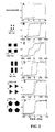
- the deviations from the Langevin model are greatest for the square symmetry nanomagnets. This is consistent with these possessing the strongest configurational anisotropy energy, meaning that the giant spin contained in a square nanomagnet looks least like a giant spin in free space. It is configurational anisotropy which eventually causes all of the symmetries to fall away from the Langevin model with increasing size.
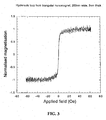
- the susceptibilities measured here are two orders of magnitude greater than would have been obtained from magnetic particles of the same shape and aspect ratio but made on a larger than nanometre lengthscale (i.e. micrometers and above, as most conventional magnetic field sensors use). In this latter case, susceptibility comes from the motion of domain walls against the internal demagnetising field, which can be very strong. The unique role of nanometre scale structuring is thus clearly demonstrated.
Landscapes
- Engineering & Computer Science (AREA)
- Chemical & Material Sciences (AREA)
- Nanotechnology (AREA)
- Physics & Mathematics (AREA)
- Crystallography & Structural Chemistry (AREA)
- Mathematical Physics (AREA)
- Computer Hardware Design (AREA)
- Condensed Matter Physics & Semiconductors (AREA)
- Power Engineering (AREA)
- Theoretical Computer Science (AREA)
- General Physics & Mathematics (AREA)
- General Engineering & Computer Science (AREA)
- Computing Systems (AREA)
- Hard Magnetic Materials (AREA)
- Hall/Mr Elements (AREA)
- Thin Magnetic Films (AREA)
- Soft Magnetic Materials (AREA)
- Measuring Magnetic Variables (AREA)
- Valve Device For Special Equipments (AREA)
- Magnetic Record Carriers (AREA)
- Transmission And Conversion Of Sensor Element Output (AREA)
- Electrochromic Elements, Electrophoresis, Or Variable Reflection Or Absorption Elements (AREA)
Abstract
Description
Claims (5)
- A magnetic logic element comprising nanomagnets having a geometric rotational symmetry around an axis selected such that they are superparamagnetic and exhibit substantially zero hysteresis so that a magnetisation of the nanomagnets depends only on the current value of applied field and not on the field history.
- A logic element according to claim 1, formed from an artificial magnetic material formed on the surface of a substrate, the axis being substantially perpendicular to the surface.
- A logic element according to claim 1 or 2, formed from Supermalloy (Ni80Fe14Mo5).
- A logic element according to any of claims 1, 2 or 3 the size range 40-500nm per side and in the thickness range 3-10nm.
- A logic element according to any of claims 1 to 4, having rotational symmetries to the order 3 or 5.
Applications Claiming Priority (4)
| Application Number | Priority Date | Filing Date | Title |
|---|---|---|---|
| GBGB9908179.6A GB9908179D0 (en) | 1999-04-09 | 1999-04-09 | Magnetic materials |
| GB9908179 | 1999-04-09 | ||
| EP04006047A EP1437746B1 (en) | 1999-04-09 | 2000-04-07 | Nanomagnetic materials |
| EP00919026A EP1169720B1 (en) | 1999-04-09 | 2000-04-07 | Magnetic materials |
Related Parent Applications (1)
| Application Number | Title | Priority Date | Filing Date |
|---|---|---|---|
| EP04006047A Division EP1437746B1 (en) | 1999-04-09 | 2000-04-07 | Nanomagnetic materials |
Publications (3)
| Publication Number | Publication Date |
|---|---|
| EP1598834A2 true EP1598834A2 (en) | 2005-11-23 |
| EP1598834A3 EP1598834A3 (en) | 2006-05-10 |
| EP1598834B1 EP1598834B1 (en) | 2008-09-17 |
Family
ID=10851267
Family Applications (3)
| Application Number | Title | Priority Date | Filing Date |
|---|---|---|---|
| EP05016528A Expired - Lifetime EP1598834B1 (en) | 1999-04-09 | 2000-04-07 | Magnetic logic element |
| EP04006047A Expired - Lifetime EP1437746B1 (en) | 1999-04-09 | 2000-04-07 | Nanomagnetic materials |
| EP00919026A Expired - Lifetime EP1169720B1 (en) | 1999-04-09 | 2000-04-07 | Magnetic materials |
Family Applications After (2)
| Application Number | Title | Priority Date | Filing Date |
|---|---|---|---|
| EP04006047A Expired - Lifetime EP1437746B1 (en) | 1999-04-09 | 2000-04-07 | Nanomagnetic materials |
| EP00919026A Expired - Lifetime EP1169720B1 (en) | 1999-04-09 | 2000-04-07 | Magnetic materials |
Country Status (15)
| Country | Link |
|---|---|
| US (1) | US6614084B1 (en) |
| EP (3) | EP1598834B1 (en) |
| JP (3) | JP4287062B2 (en) |
| KR (1) | KR100699611B1 (en) |
| CN (1) | CN1251251C (en) |
| AT (3) | ATE341821T1 (en) |
| AU (1) | AU763157B2 (en) |
| CA (1) | CA2366588A1 (en) |
| DE (3) | DE60031181T2 (en) |
| DK (1) | DK1169720T3 (en) |
| ES (1) | ES2225119T3 (en) |
| GB (1) | GB9908179D0 (en) |
| PT (1) | PT1169720E (en) |
| RU (3) | RU2244971C2 (en) |
| WO (1) | WO2000062311A1 (en) |
Families Citing this family (13)
| Publication number | Priority date | Publication date | Assignee | Title |
|---|---|---|---|---|
| GB9925213D0 (en) | 1999-10-25 | 1999-12-22 | Univ Cambridge Tech | Magnetic logic elements |
| US7733350B2 (en) * | 2006-06-30 | 2010-06-08 | Microsoft Corporation | Anisometric texture synthesis |
| US8134441B1 (en) * | 2008-06-02 | 2012-03-13 | The Regents Of The University Of California | Nanomagnetic signal propagation and logic gates |
| US8138874B1 (en) | 2009-07-20 | 2012-03-20 | The Regents Of The University Of California | Nanomagnetic register |
| WO2011044100A2 (en) * | 2009-10-05 | 2011-04-14 | University Of Delaware | Ferromagnetic resonance and memory effect in magnetic composite materials |
| US9196280B2 (en) * | 2009-11-12 | 2015-11-24 | Marquette University | Low-field magnetic domain wall injection pad and high-density storage wire |
| KR200452028Y1 (en) * | 2010-02-23 | 2011-02-01 | 정진시그널(주) | Road sign with transparent reflector |
| US8766754B2 (en) | 2012-07-18 | 2014-07-01 | The Regents Of The University Of California | Concave nanomagnets with widely tunable anisotropy |
| US9460737B2 (en) | 2013-04-18 | 2016-10-04 | Headway Technologies, Inc. | Supermalloy and mu metal side and top shields for magnetic read heads |
| FR3031622B1 (en) * | 2015-01-14 | 2018-02-16 | Centre National De La Recherche Scientifique | MAGNETIC MEMORY POINT |
| JP6821665B2 (en) * | 2015-06-04 | 2021-01-27 | エンドマグネティクス リミテッド | Magnetic marker |
| JP7565563B2 (en) * | 2021-05-14 | 2024-10-11 | 国立大学法人東北大学 | Magnetic metamaterial, spin current control device and spin current control method |
| CN119626285B (en) * | 2024-11-06 | 2025-07-18 | 云南大学 | Magnetic nano multi-ring memory device and preparation method and application thereof |
Family Cites Families (17)
| Publication number | Priority date | Publication date | Assignee | Title |
|---|---|---|---|---|
| US3873914A (en) * | 1973-07-18 | 1975-03-25 | Sperry Rand Corp | Flux valve apparatus for sensing both horizontal and vertical components of an ambient magnetic field |
| RU2006965C1 (en) * | 1990-08-09 | 1994-01-30 | Московский институт электронной техники | Read-only storage item |
| JPH0810653B2 (en) * | 1990-11-22 | 1996-01-31 | 科学技術庁金属材料技術研究所長 | Array lattice structure of magnetic particles |
| RU2029391C1 (en) * | 1991-06-28 | 1995-02-20 | Тимошков Юрий Викторович | Storage element |
| US5710436A (en) | 1994-09-27 | 1998-01-20 | Kabushiki Kaisha Toshiba | Quantum effect device |
| US5654566A (en) * | 1995-04-21 | 1997-08-05 | Johnson; Mark B. | Magnetic spin injected field effect transistor and method of operation |
| RU2093905C1 (en) * | 1995-05-23 | 1997-10-20 | Институт проблем управления РАН | Gate with memory |
| US5741435A (en) * | 1995-08-08 | 1998-04-21 | Nano Systems, Inc. | Magnetic memory having shape anisotropic magnetic elements |
| US5714536A (en) * | 1996-01-11 | 1998-02-03 | Xerox Corporation | Magnetic nanocompass compositions and processes for making and using |
| JPH09298320A (en) * | 1996-05-09 | 1997-11-18 | Kobe Steel Ltd | Persistent current switch for oxide superconducting coil, switch device using the same, and switching method |
| RU2120142C1 (en) * | 1996-07-02 | 1998-10-10 | Институт проблем управления РАН | Magnetic inverter |
| US6451220B1 (en) * | 1997-01-21 | 2002-09-17 | Xerox Corporation | High density magnetic recording compositions and processes thereof |
| JPH10326920A (en) * | 1997-03-26 | 1998-12-08 | Delta Tsuuring:Kk | Magnetoresistive sensor and method of manufacturing the same |
| JPH1179894A (en) * | 1997-09-04 | 1999-03-23 | Mitsubishi Gas Chem Co Inc | Bismuth substituted rare earth iron garnet single crystal film |
| US5898549A (en) * | 1997-10-27 | 1999-04-27 | International Business Machines Corporation | Anti-parallel-pinned spin valve sensor with minimal pinned layer shunting |
| JP3216605B2 (en) * | 1998-07-06 | 2001-10-09 | 日本電気株式会社 | Dot array-like magnetic film, magnetic recording medium and magnetoresistive element using the same |
| US6269018B1 (en) * | 2000-04-13 | 2001-07-31 | International Business Machines Corporation | Magnetic random access memory using current through MTJ write mechanism |
-
1999
- 1999-04-09 GB GBGB9908179.6A patent/GB9908179D0/en not_active Ceased
-
2000
- 2000-04-07 AT AT04006047T patent/ATE341821T1/en not_active IP Right Cessation
- 2000-04-07 EP EP05016528A patent/EP1598834B1/en not_active Expired - Lifetime
- 2000-04-07 EP EP04006047A patent/EP1437746B1/en not_active Expired - Lifetime
- 2000-04-07 DE DE60031181T patent/DE60031181T2/en not_active Expired - Lifetime
- 2000-04-07 DE DE60040307T patent/DE60040307D1/en not_active Expired - Lifetime
- 2000-04-07 JP JP2000611293A patent/JP4287062B2/en not_active Expired - Fee Related
- 2000-04-07 CA CA002366588A patent/CA2366588A1/en not_active Abandoned
- 2000-04-07 EP EP00919026A patent/EP1169720B1/en not_active Expired - Lifetime
- 2000-04-07 AU AU39785/00A patent/AU763157B2/en not_active Ceased
- 2000-04-07 US US09/958,318 patent/US6614084B1/en not_active Expired - Fee Related
- 2000-04-07 AT AT00919026T patent/ATE272889T1/en not_active IP Right Cessation
- 2000-04-07 KR KR1020017012844A patent/KR100699611B1/en not_active Expired - Fee Related
- 2000-04-07 DE DE60012720T patent/DE60012720T2/en not_active Expired - Lifetime
- 2000-04-07 CN CNB008060711A patent/CN1251251C/en not_active Expired - Fee Related
- 2000-04-07 DK DK00919026T patent/DK1169720T3/en active
- 2000-04-07 RU RU2001130141/02A patent/RU2244971C2/en not_active IP Right Cessation
- 2000-04-07 PT PT00919026T patent/PT1169720E/en unknown
- 2000-04-07 ES ES00919026T patent/ES2225119T3/en not_active Expired - Lifetime
- 2000-04-07 WO PCT/GB2000/001306 patent/WO2000062311A1/en not_active Ceased
- 2000-04-07 AT AT05016528T patent/ATE408885T1/en not_active IP Right Cessation
-
2004
- 2004-01-16 RU RU2004101439/02A patent/RU2274917C2/en not_active IP Right Cessation
-
2005
- 2005-04-21 RU RU2005112055/02A patent/RU2005112055A/en not_active Application Discontinuation
-
2008
- 2008-04-25 JP JP2008115325A patent/JP2009002937A/en active Pending
- 2008-04-25 JP JP2008115326A patent/JP2008288580A/en not_active Withdrawn
Also Published As
Similar Documents
| Publication | Publication Date | Title |
|---|---|---|
| JP2009002937A (en) | Sensor element | |
| Cowburn et al. | Designing nanostructured magnetic materials by symmetry | |
| JP4568926B2 (en) | Magnetic functional element and magnetic recording apparatus | |
| JP3574186B2 (en) | Magnetoresistance effect element | |
| JP2003016620A (en) | Magnetic recording medium, magnetic recording device, and magnetic recording method | |
| JP2003296901A (en) | Magnetic recording device and magnetic recording method | |
| KR20040076819A (en) | Magnetic recording media with write-assist layer | |
| JPH0268906A (en) | High saturation magnetic flux density soft magnetic film and magnetic head | |
| JP2003091801A (en) | Magnetic recording device and magnetic recording medium | |
| JP2924798B2 (en) | Magnetoresistance thin film | |
| Cowburn et al. | Sensing magnetic fields using superparamagnetic nanomagnets | |
| WO1999050833A1 (en) | Method and apparatus for magnetic recording | |
| JP2003085702A (en) | Magnetic recording device | |
| JPS60101710A (en) | Vertical magnetic recording medium | |
| JP3547974B2 (en) | Magnetic element, magnetic head and magnetic storage device using the same | |
| AU2003204184B2 (en) | Magnetic materials | |
| JP3455055B2 (en) | Magnetic element, magnetic head and magnetic storage device using the same | |
| US5872690A (en) | Magnetic transducer and magnetic recording device utilizing material in which undirectional anisotropy can be formed | |
| JPH0217846B2 (en) | ||
| Pardavi-Horvath | Stability of Magnetic States in Patterned Materials | |
| JPS6095721A (en) | Vertical magnetic recording medium and its production | |
| JPH04214207A (en) | Multilayer magneto-resistance-effect film and magneto-resistance-effect element using the film | |
| HK1025180A (en) | A shield in a read element in a magnetic data head | |
| GB2343054A (en) | A shield in a read element in a magnetic data head |
Legal Events
| Date | Code | Title | Description |
|---|---|---|---|
| PUAI | Public reference made under article 153(3) epc to a published international application that has entered the european phase |
Free format text: ORIGINAL CODE: 0009012 |
|
| 17P | Request for examination filed |
Effective date: 20050818 |
|
| AC | Divisional application: reference to earlier application |
Ref document number: 1169720 Country of ref document: EP Kind code of ref document: P Ref document number: 1437746 Country of ref document: EP Kind code of ref document: P |
|
| AK | Designated contracting states |
Kind code of ref document: A2 Designated state(s): AT BE CH CY DE DK ES FI FR GB GR IE IT LI LU MC NL PT SE |
|
| PUAL | Search report despatched |
Free format text: ORIGINAL CODE: 0009013 |
|
| AK | Designated contracting states |
Kind code of ref document: A3 Designated state(s): AT BE CH CY DE DK ES FI FR GB GR IE IT LI LU MC NL PT SE |
|
| RAP1 | Party data changed (applicant data changed or rights of an application transferred) |
Owner name: CAMBRIDGE ENTERPRISE LIMITED |
|
| AKX | Designation fees paid |
Designated state(s): AT BE CH CY DE DK ES FI FR GB GR IE IT LI LU MC NL PT SE |
|
| 17Q | First examination report despatched |
Effective date: 20070111 |
|
| GRAP | Despatch of communication of intention to grant a patent |
Free format text: ORIGINAL CODE: EPIDOSNIGR1 |
|
| RIC1 | Information provided on ipc code assigned before grant |
Ipc: H03K 19/16 20060101ALI20080211BHEP Ipc: G06N 1/00 20060101ALI20080211BHEP Ipc: H01F 1/00 20060101AFI20080211BHEP |
|
| RTI1 | Title (correction) |
Free format text: MAGNETIC LOGIC ELEMENT |
|
| GRAS | Grant fee paid |
Free format text: ORIGINAL CODE: EPIDOSNIGR3 |
|
| GRAA | (expected) grant |
Free format text: ORIGINAL CODE: 0009210 |
|
| AC | Divisional application: reference to earlier application |
Ref document number: 1169720 Country of ref document: EP Kind code of ref document: P Ref document number: 1437746 Country of ref document: EP Kind code of ref document: P |
|
| AK | Designated contracting states |
Kind code of ref document: B1 Designated state(s): AT BE CH CY DE DK ES FI FR GB GR IE IT LI LU MC NL PT SE |
|
| REG | Reference to a national code |
Ref country code: GB Ref legal event code: FG4D |
|
| REG | Reference to a national code |
Ref country code: CH Ref legal event code: EP |
|
| REG | Reference to a national code |
Ref country code: IE Ref legal event code: FG4D |
|
| REF | Corresponds to: |
Ref document number: 60040307 Country of ref document: DE Date of ref document: 20081030 Kind code of ref document: P |
|
| PG25 | Lapsed in a contracting state [announced via postgrant information from national office to epo] |
Ref country code: FI Free format text: LAPSE BECAUSE OF FAILURE TO SUBMIT A TRANSLATION OF THE DESCRIPTION OR TO PAY THE FEE WITHIN THE PRESCRIBED TIME-LIMIT Effective date: 20080917 Ref country code: AT Free format text: LAPSE BECAUSE OF FAILURE TO SUBMIT A TRANSLATION OF THE DESCRIPTION OR TO PAY THE FEE WITHIN THE PRESCRIBED TIME-LIMIT Effective date: 20080917 |
|
| NLV1 | Nl: lapsed or annulled due to failure to fulfill the requirements of art. 29p and 29m of the patents act | ||
| PG25 | Lapsed in a contracting state [announced via postgrant information from national office to epo] |
Ref country code: BE Free format text: LAPSE BECAUSE OF FAILURE TO SUBMIT A TRANSLATION OF THE DESCRIPTION OR TO PAY THE FEE WITHIN THE PRESCRIBED TIME-LIMIT Effective date: 20080917 |
|
| PG25 | Lapsed in a contracting state [announced via postgrant information from national office to epo] |
Ref country code: ES Free format text: LAPSE BECAUSE OF FAILURE TO SUBMIT A TRANSLATION OF THE DESCRIPTION OR TO PAY THE FEE WITHIN THE PRESCRIBED TIME-LIMIT Effective date: 20081228 |
|
| PG25 | Lapsed in a contracting state [announced via postgrant information from national office to epo] |
Ref country code: PT Free format text: LAPSE BECAUSE OF FAILURE TO SUBMIT A TRANSLATION OF THE DESCRIPTION OR TO PAY THE FEE WITHIN THE PRESCRIBED TIME-LIMIT Effective date: 20090217 Ref country code: NL Free format text: LAPSE BECAUSE OF FAILURE TO SUBMIT A TRANSLATION OF THE DESCRIPTION OR TO PAY THE FEE WITHIN THE PRESCRIBED TIME-LIMIT Effective date: 20080917 |
|
| PLBE | No opposition filed within time limit |
Free format text: ORIGINAL CODE: 0009261 |
|
| STAA | Information on the status of an ep patent application or granted ep patent |
Free format text: STATUS: NO OPPOSITION FILED WITHIN TIME LIMIT |
|
| PG25 | Lapsed in a contracting state [announced via postgrant information from national office to epo] |
Ref country code: DK Free format text: LAPSE BECAUSE OF FAILURE TO SUBMIT A TRANSLATION OF THE DESCRIPTION OR TO PAY THE FEE WITHIN THE PRESCRIBED TIME-LIMIT Effective date: 20080917 |
|
| 26N | No opposition filed |
Effective date: 20090618 |
|
| PG25 | Lapsed in a contracting state [announced via postgrant information from national office to epo] |
Ref country code: IT Free format text: LAPSE BECAUSE OF FAILURE TO SUBMIT A TRANSLATION OF THE DESCRIPTION OR TO PAY THE FEE WITHIN THE PRESCRIBED TIME-LIMIT Effective date: 20080917 |
|
| REG | Reference to a national code |
Ref country code: CH Ref legal event code: PL |
|
| PG25 | Lapsed in a contracting state [announced via postgrant information from national office to epo] |
Ref country code: CH Free format text: LAPSE BECAUSE OF NON-PAYMENT OF DUE FEES Effective date: 20090430 Ref country code: LI Free format text: LAPSE BECAUSE OF NON-PAYMENT OF DUE FEES Effective date: 20090430 Ref country code: SE Free format text: LAPSE BECAUSE OF FAILURE TO SUBMIT A TRANSLATION OF THE DESCRIPTION OR TO PAY THE FEE WITHIN THE PRESCRIBED TIME-LIMIT Effective date: 20081217 |
|
| REG | Reference to a national code |
Ref country code: IE Ref legal event code: MM4A |
|
| PG25 | Lapsed in a contracting state [announced via postgrant information from national office to epo] |
Ref country code: MC Free format text: LAPSE BECAUSE OF NON-PAYMENT OF DUE FEES Effective date: 20090430 Ref country code: IE Free format text: LAPSE BECAUSE OF NON-PAYMENT OF DUE FEES Effective date: 20090407 |
|
| PGFP | Annual fee paid to national office [announced via postgrant information from national office to epo] |
Ref country code: GB Payment date: 20100311 Year of fee payment: 11 |
|
| PGFP | Annual fee paid to national office [announced via postgrant information from national office to epo] |
Ref country code: FR Payment date: 20100415 Year of fee payment: 11 |
|
| PGFP | Annual fee paid to national office [announced via postgrant information from national office to epo] |
Ref country code: DE Payment date: 20100610 Year of fee payment: 11 |
|
| PG25 | Lapsed in a contracting state [announced via postgrant information from national office to epo] |
Ref country code: GR Free format text: LAPSE BECAUSE OF FAILURE TO SUBMIT A TRANSLATION OF THE DESCRIPTION OR TO PAY THE FEE WITHIN THE PRESCRIBED TIME-LIMIT Effective date: 20081218 |
|
| PG25 | Lapsed in a contracting state [announced via postgrant information from national office to epo] |
Ref country code: LU Free format text: LAPSE BECAUSE OF NON-PAYMENT OF DUE FEES Effective date: 20090407 |
|
| PG25 | Lapsed in a contracting state [announced via postgrant information from national office to epo] |
Ref country code: CY Free format text: LAPSE BECAUSE OF FAILURE TO SUBMIT A TRANSLATION OF THE DESCRIPTION OR TO PAY THE FEE WITHIN THE PRESCRIBED TIME-LIMIT Effective date: 20080917 |
|
| GBPC | Gb: european patent ceased through non-payment of renewal fee |
Effective date: 20110407 |
|
| REG | Reference to a national code |
Ref country code: FR Ref legal event code: ST Effective date: 20111230 |
|
| PG25 | Lapsed in a contracting state [announced via postgrant information from national office to epo] |
Ref country code: DE Free format text: LAPSE BECAUSE OF NON-PAYMENT OF DUE FEES Effective date: 20111101 Ref country code: FR Free format text: LAPSE BECAUSE OF NON-PAYMENT OF DUE FEES Effective date: 20110502 |
|
| REG | Reference to a national code |
Ref country code: DE Ref legal event code: R119 Ref document number: 60040307 Country of ref document: DE Effective date: 20111101 |
|
| PG25 | Lapsed in a contracting state [announced via postgrant information from national office to epo] |
Ref country code: GB Free format text: LAPSE BECAUSE OF NON-PAYMENT OF DUE FEES Effective date: 20110407 |