EP1598141A1 - Methods for laser processing - Google Patents
Methods for laser processing Download PDFInfo
- Publication number
- EP1598141A1 EP1598141A1 EP05252943A EP05252943A EP1598141A1 EP 1598141 A1 EP1598141 A1 EP 1598141A1 EP 05252943 A EP05252943 A EP 05252943A EP 05252943 A EP05252943 A EP 05252943A EP 1598141 A1 EP1598141 A1 EP 1598141A1
- Authority
- EP
- European Patent Office
- Prior art keywords
- substrate
- supplying
- act
- layer assembly
- layer
- Prior art date
- Legal status (The legal status is an assumption and is not a legal conclusion. Google has not performed a legal analysis and makes no representation as to the accuracy of the status listed.)
- Withdrawn
Links
- 238000000034 method Methods 0.000 title claims description 43
- 238000012545 processing Methods 0.000 title description 37
- 239000000758 substrate Substances 0.000 claims abstract description 78
- 239000012530 fluid Substances 0.000 claims description 42
- 239000000463 material Substances 0.000 claims description 40
- 238000003754 machining Methods 0.000 claims description 33
- 239000007788 liquid Substances 0.000 claims description 14
- XLYOFNOQVPJJNP-UHFFFAOYSA-N water Substances O XLYOFNOQVPJJNP-UHFFFAOYSA-N 0.000 claims description 11
- 230000003287 optical effect Effects 0.000 claims description 5
- 230000007423 decrease Effects 0.000 claims description 2
- 239000004020 conductor Substances 0.000 abstract description 11
- 239000010410 layer Substances 0.000 description 91
- 239000011241 protective layer Substances 0.000 description 30
- 239000010409 thin film Substances 0.000 description 22
- 230000004888 barrier function Effects 0.000 description 21
- 238000004519 manufacturing process Methods 0.000 description 14
- 238000007639 printing Methods 0.000 description 9
- 238000010304 firing Methods 0.000 description 8
- 235000012431 wafers Nutrition 0.000 description 8
- 238000012546 transfer Methods 0.000 description 5
- 229920000642 polymer Polymers 0.000 description 4
- 239000004372 Polyvinyl alcohol Substances 0.000 description 3
- 238000005516 engineering process Methods 0.000 description 3
- 239000010408 film Substances 0.000 description 3
- 229920002451 polyvinyl alcohol Polymers 0.000 description 3
- PXHVJJICTQNCMI-UHFFFAOYSA-N Nickel Chemical compound [Ni] PXHVJJICTQNCMI-UHFFFAOYSA-N 0.000 description 2
- 230000005540 biological transmission Effects 0.000 description 2
- 230000015556 catabolic process Effects 0.000 description 2
- 238000000576 coating method Methods 0.000 description 2
- 230000002950 deficient Effects 0.000 description 2
- 239000011888 foil Substances 0.000 description 2
- 239000007789 gas Substances 0.000 description 2
- 230000007246 mechanism Effects 0.000 description 2
- 229910052751 metal Inorganic materials 0.000 description 2
- 239000002184 metal Substances 0.000 description 2
- 239000011148 porous material Substances 0.000 description 2
- 239000000523 sample Substances 0.000 description 2
- JBRZTFJDHDCESZ-UHFFFAOYSA-N AsGa Chemical compound [As]#[Ga] JBRZTFJDHDCESZ-UHFFFAOYSA-N 0.000 description 1
- 229910005540 GaP Inorganic materials 0.000 description 1
- 229910001218 Gallium arsenide Inorganic materials 0.000 description 1
- GPXJNWSHGFTCBW-UHFFFAOYSA-N Indium phosphide Chemical compound [In]#P GPXJNWSHGFTCBW-UHFFFAOYSA-N 0.000 description 1
- 229920003171 Poly (ethylene oxide) Polymers 0.000 description 1
- 238000009825 accumulation Methods 0.000 description 1
- 238000013459 approach Methods 0.000 description 1
- 230000001680 brushing effect Effects 0.000 description 1
- 239000011248 coating agent Substances 0.000 description 1
- 238000004132 cross linking Methods 0.000 description 1
- 230000003247 decreasing effect Effects 0.000 description 1
- 238000006731 degradation reaction Methods 0.000 description 1
- 238000003618 dip coating Methods 0.000 description 1
- 238000004070 electrodeposition Methods 0.000 description 1
- HZXMRANICFIONG-UHFFFAOYSA-N gallium phosphide Chemical compound [Ga]#P HZXMRANICFIONG-UHFFFAOYSA-N 0.000 description 1
- 239000011521 glass Substances 0.000 description 1
- 238000002513 implantation Methods 0.000 description 1
- 238000010348 incorporation Methods 0.000 description 1
- 238000010030 laminating Methods 0.000 description 1
- 238000000608 laser ablation Methods 0.000 description 1
- 230000007257 malfunction Effects 0.000 description 1
- 238000005259 measurement Methods 0.000 description 1
- 238000004377 microelectronic Methods 0.000 description 1
- 229910052759 nickel Inorganic materials 0.000 description 1
- 239000002861 polymer material Substances 0.000 description 1
- 229920002689 polyvinyl acetate Polymers 0.000 description 1
- 239000011118 polyvinyl acetate Substances 0.000 description 1
- 230000002035 prolonged effect Effects 0.000 description 1
- 239000011253 protective coating Substances 0.000 description 1
- 229910052710 silicon Inorganic materials 0.000 description 1
- 239000010703 silicon Substances 0.000 description 1
- 239000007787 solid Substances 0.000 description 1
- 238000005507 spraying Methods 0.000 description 1
- 238000004544 sputter deposition Methods 0.000 description 1
- 229920001169 thermoplastic Polymers 0.000 description 1
- 239000004416 thermosoftening plastic Substances 0.000 description 1
Images




Classifications
-
- B—PERFORMING OPERATIONS; TRANSPORTING
- B23—MACHINE TOOLS; METAL-WORKING NOT OTHERWISE PROVIDED FOR
- B23K—SOLDERING OR UNSOLDERING; WELDING; CLADDING OR PLATING BY SOLDERING OR WELDING; CUTTING BY APPLYING HEAT LOCALLY, e.g. FLAME CUTTING; WORKING BY LASER BEAM
- B23K26/00—Working by laser beam, e.g. welding, cutting or boring
- B23K26/14—Working by laser beam, e.g. welding, cutting or boring using a fluid stream, e.g. a jet of gas, in conjunction with the laser beam; Nozzles therefor
- B23K26/146—Working by laser beam, e.g. welding, cutting or boring using a fluid stream, e.g. a jet of gas, in conjunction with the laser beam; Nozzles therefor the fluid stream containing a liquid
-
- B—PERFORMING OPERATIONS; TRANSPORTING
- B23—MACHINE TOOLS; METAL-WORKING NOT OTHERWISE PROVIDED FOR
- B23K—SOLDERING OR UNSOLDERING; WELDING; CLADDING OR PLATING BY SOLDERING OR WELDING; CUTTING BY APPLYING HEAT LOCALLY, e.g. FLAME CUTTING; WORKING BY LASER BEAM
- B23K26/00—Working by laser beam, e.g. welding, cutting or boring
- B23K26/36—Removing material
- B23K26/38—Removing material by boring or cutting
- B23K26/382—Removing material by boring or cutting by boring
- B23K26/389—Removing material by boring or cutting by boring of fluid openings, e.g. nozzles, jets
Definitions
- Integrated circuits comprise a substrate over which other various layers are positioned to form the integrated circuit.
- Various substrate removal techniques can be utilized during processing.
- One production technique involves laser machining to selectively remove substrate material.
- laser machining can be useful in various production applications including forming slotted substrates configured for incorporation into various fluid-ejecting devices.
- fluid-ejecting devices can be adapted to various applications including print heads for ink jet print cartridges, as well as various other laboratory and medical applications.
- Laser machining can also be useful in other production applications, such as dicing of wafers into individual substrates. While laser machining is a useful production technique, present laser machining techniques can cause incidental damage to component layers positioned on a substrate during laser processing. Thus a need exists for improved laser processing technologies.
- Fig. 1 illustrates a front elevational view of a diagrammatic representation of an exemplary printer in accordance with one exemplary embodiment.
- Fig. 2 illustrates a perspective view of a diagrammatic representation of a print cartridge suitable for use in the exemplary printer shown in Fig. 1 in accordance with one exemplary embodiment.
- Fig. 3 illustrates a diagrammatic representation of a side-sectional view of a portion of the print cartridge shown in Fig. 2 in accordance with one exemplary embodiment.
- Figs. 4a-4f illustrate diagrammatic representations of process steps for laser processing an exemplary slotted substrate in accordance with one embodiment.
- Fig. 5a illustrates a diagrammatic representation of a process step for laser processing an exemplary slotted substrate in accordance with one embodiment.
- Fig. 6a illustrates a diagrammatic representation of a process step for laser processing an exemplary slotted substrate in accordance with one embodiment.
- Figs. 7a-7d illustrate diagrammatic representations of process steps for laser processing to separate individual substrates in accordance with one embodiment.
- the embodiments described below pertain to methods and systems for laser processing of integrated circuits.
- the integrated circuits comprise a substrate having various layers positioned thereon.
- Laser processing can be utilized to form a feature such as a slot, trench or other through or blind feature, within an individual integrated circuit.
- laser processing can be utilized to separate integrated circuits from one another.
- the embodiments described below allow the laser machining process to produce high quality substrates and associated layers.
- Fig. 1 illustrates a diagrammatic representation of an exemplary printing device that can utilize an exemplary print cartridge.
- the printing device comprises a printer 100.
- the printer shown here is embodied in the form of an inkjet printer.
- the printer 100 can be capable of printing in black-and-white and color.
- the term "printing device" refers to any type of printing device and/or image forming device that employs slotted substrate(s) to achieve at least a portion of its functionality. Examples of such printing devices can include, but are not limited to, printers, facsimile machines, and photocopiers.
- the slotted substrates comprise a portion of a print head which is incorporated into a print cartridge, an example of which is described below.
- Fig. 2 shows a diagrammatic representation of an exemplary print cartridge 202 that can be utilized in an exemplary printing device.
- the print cartridge is comprised of a print head 204 and a cartridge body 206 that supports the print head.
- Print head 204 comprises an example of an integrated circuit in the form of a fluid-ejecting device. Though a single print head 204 is employed on this print cartridge 202 other exemplary configurations may employ multiple print heads on a single cartridge.
- Print cartridge 202 is configured to have a self-contained fluid or ink supply within cartridge body 206.
- Other print cartridge configurations may alternatively or additionally be configured to receive fluid from an external supply.
- Other exemplary configurations will be recognized by those of skill in the art.
- Print cartridge failure can be brought about by defective or faulty print cartridge components. Such component failure can be caused by among other factors damage to print cartridge components during manufacture. As such, various embodiments described below can provide print heads with a reduced propensity for failure.
- Fig. 3 shows a cross-sectional diagrammatic representation of a portion of the exemplary print head 204, taken along line 3-3 in Fig. 2.
- a substrate 300 extends between a first substrate surface ("first surface”) 302 and a second substrate surface ("second surface”) 303 to define a thickness t there between.
- a slot 305 passes through substrate 300 between first and second surfaces 302, 303.
- the view of Fig. 3 is taken transverse an x -axis of slot 305.
- the x -axis comprises a long axis extending into and out of the plane of the page upon which Fig. 3 appears.
- substrate 300 comprises silicon which can be either doped or undoped.
- suitable substrate materials can include, but are not limited to, gallium arsenide, gallium phosphide, indium phosphide, glass or other material.
- Substrate thicknesses t can have any suitable dimensions that are appropriate for substrates' intended applications. In some embodiments, substrate thicknesses taken relative to the z-direction can range from less than 100 microns to more than 2000 microns. One exemplary embodiment can utilize a substrate that is approximately 675 microns thick. Though a single substrate is discussed herein, other suitable embodiments may comprise a substrate that has multiple components during assembly and/or in the finished product. For example, one such embodiment may employ a substrate having a first component and a second sacrificial component which is discarded at some point during processing.
- a layer assembly 307 comprising one or more layers is formed over the second surface 303 of the substrate.
- layer assembly 307 comprises a first sub-assembly 311 of one or more layers, and a second sub-assembly 312 of one or more layers.
- first sub-assembly 311 comprises one or more thin-film layers 314, and second sub-assembly 312 comprises one or more thick-film layers, which in one embodiment comprise a photo-imagable polymer.
- the second sub-assembly 312 comprises a barrier layer 316 and an orifice plate or orifice layer 318.
- one or more thin-film layers 314 can be patterned to comprise one or more electrical components such as electrical traces (not specifically shown) resistors 320 and transistors (not specifically shown). Individual resistors can be selectively controlled via the electrical traces.
- Thin-film layers 314 can in some embodiments also define, at least in part, a wall or surface of multiple fluid-feed passageways 322 through which fluid can pass.
- Barrier layer 316 can define, at least in part, multiple firing chambers 324.
- barrier layer 316 may, in combination with thin-film layers 314, define fluid-feed passageways 322.
- Orifice layer 318 can define multiple firing nozzles 326. Individual firing nozzles can be respectively aligned with individual firing chambers 324.
- Barrier layer 316 and orifice layer 318 can be formed in any suitable manner.
- both barrier layer 316 and orifice layer 318 comprise thick-film material, such as a photo-imagable polymer material.
- the material can be applied in any suitable manner.
- the material can be "spun-on" as will be recognized by the skilled artisan.
- barrier layer 316 can then be patterned to form, at least in part, desired features, such as firing chambers 324, therein.
- patterned areas of the barrier layer can be filled with a sacrificial material.
- orifice layer 318 can be comprised of the same material as the barrier layer and be formed over barrier layer 316. In one such example, orifice layer material is 'spun-on' over the barrier layer. Orifice layer 318 can then be patterned as desired to form nozzles 326 over respective chambers 324. The sacrificial material is then removed from the barrier layer's chambers 324 and passageways 322.
- barrier layer 316 comprises a thick-film
- orifice layer 318 comprises an electroformed nickel material.
- Other suitable embodiments may employ an orifice layer which performs the functions of both a barrier layer and an orifice layer.
- fluid such as ink can enter slot 305 from the cartridge body, shown Fig. 2. Fluid can then flow through individual passageways 322 into an individual chamber 324. Fluid can be ejected from the chamber when an electrical current is passed through an individual resistor 320. The electrical current can heat the resistor sufficiently to vaporize some of the fluid contained in the firing chamber so that it expands to eject a portion of the remaining fluid from a respectively positioned nozzle 326. The ejected fluid can then be replaced by additional fluid from passageway 322.
- Figs. 4a-4f illustrate production techniques for producing an exemplary print head similar to print head 204 shown in Fig. 3.
- the skilled artisan should recognize that the production techniques described below are equally applicable to other types of fluid-ejecting devices or other microelectronic devices in which features are formed.
- fabricating an exemplary print head begins with a substrate 300a. Various characteristics of the substrate are described above. Various thin-film layers 314a are positioned over second surface 303a in a manner known in the art to form various electrical components. In some embodiments, the thin-film layers 314a comprise at least one patterned conductive layer and at least one dielectric layer. In other embodiments thin-film layers 314a may include anti-cavitation and/or other protective layers as are known in the art.
- barrier layer 316a Positioned over thin-films 314a is barrier layer 316a.
- the barrier layer may be patterned at this point to form the various firing chambers described above in relation to Fig. 3. Alternatively, the firing chambers may be formed at a subsequent point in the processing.
- one or more protective layer(s) or coating(s) 402 is positioned over barrier layer 316a.
- Protective layer 402 is intended to physically protect the underlying layers during laser processing.
- protective layer 402 can protect the underlying layers from debris produced during laser machining. Without protective layer 402, such debris can become trapped in the underlying layers and cause fluidic and/or electrical failure.
- debris produced during laser processing can become lodged in the fluid-feed passageways 322 as described in Fig. 3. The debris can subsequently occlude or obstruct ink flow through the affected passageways resulting in a malfunction during printing.
- Suitable protective layer materials can be applied before laser processing and removed after laser processing.
- Suitable protective layer materials can include various polymers such as thermoplastics and cross-linking polymers among others.
- protective layer 402 comprises polyvinyl alcohol.
- Other suitable materials for protective layers can include but are not limited to polyvinyl acetate, polyethylene oxide, and polyethyleneterathalate, among others.
- Processing techniques which utilize optical alignment equipment can utilize materials such as polyvinyl alcohol which allow sufficient optical transmission for the equipment to operate.
- materials such as polyvinyl alcohol which allow sufficient optical transmission for the equipment to operate.
- the protective layer should allow sufficient light transmission for proper equipment functioning.
- Protective layer 402 can be formed from a polyvinyl alcohol water solution that is commercially available from ATMI. The solution can be applied and then dried before laser processing. Upon completion of laser processing pressurized water and/or mechanical means such as brushing in the presence of water can be utilized to remove the protective layer. Protective layer 402 can be applied utilizing any suitable technique. In one embodiment protective layer 402 is spun-on. Other suitable embodiments may apply the protective layer by laminating, dip coating, electrocoating, sputter coating or spray coating, among other processes. In one embodiment, thin-films 314a, barrier layer 318a and protective layer 402 comprise layer assembly 307a.
- a laser beam 404 is directed at substrate 300a. Any suitable laser beam configured to remove substrate material can be utilized. Laser beam 404 is directed through the substrate's first surface 302a from a direction sufficient to contact first surface 302a before contacting the second surface 303a. Laser beam 404 is directed at a laser machining region 406 of substrate material and the laser energy removes substrate material so that laser machining region 406 progressively moves toward second surface 303a.
- the removed substrate material defines a feature 408 having a generally uniform width w throughout its depth d as defined between sidewalls 410, 412. In other embodiments, the width of the feature may vary along its depth d.
- laser machining region 406 can be defined laterally as extending between sidewalls 410, 412.
- laser machining region 406 can include substrate material defining sidewalls 410, 412 that was directly affected but not removed by the laser beam.
- the laser machining region may be defined to include substrate material proximate the feature but not removed by the laser machining process.
- the laser machining region may be in the range of 1-10 microns wider than feature width w and include what can be known as a "heat affected zone".
- Fig. 4c illustrates an enlarged region of the substrate illustrated in Fig. 4b.
- laser machining region 406 now comprises substrate material defining second surface 303a and portions of layer assembly 307a.
- laser energy directed at laser machining region 406 may unintentionally be transferred to substrate material and/or layer assembly 307a outside of laser machining region 406. Such energy transfer can damage thin-film layers 314a among others.
- Such energy transfer can damage regions of the thin-films or other components of the layer assembly 307 that are located from about 10 microns to about 125 microns away from the laser machining region. Thus, some of the unintended energy transfer can damage portions of the layer assembly 307a at locations an order of magnitude beyond the heat affected zone.
- the described embodiments reduce or eliminate damage caused by unintended energy transfer by supplying an electrically conductive material 414 proximate second surface 303a during at least a portion of the laser machining process.
- Suitable electrically conductive materials 414 can include fluids and solids among others. Several exemplary materials and methods of use are described below.
- the present embodiment reduces or eliminates damage to the layer assembly 307 by supplying an electrically conductive material 414 comprising fluid 416.
- the fluid is directed toward second surface 303a.
- Fluid 416 can itself be conductive and/or can contain material(s) which makes the fluid conductive.
- the fluid comprises ionized water having a conductivity of about 100 micro Siemens per centimeter and delivered as atomized water droplets. The ionized water is delivered at a rate of about 8 milliliters/minute.
- suitable fluids 416 can be utilized in various embodiments.
- a highly viscous and/or tacky liquid may be utilized which will may adhere to the layer assembly for a prolonged period of time during processing and as such may be supplied periodically rather than generally continuously during laser processing.
- Other suitable conductive fluids can comprise gases having sufficient rates of conductivity.
- some embodiments may utilize supersaturated gases or vapors as the conductive fluid.
- conductive fluid 416 is supplied from an atomizing nozzle 418 and from a direction sufficient to contact first surface 302a before contacting the second surface 303a.
- conductive fluid 416 flows across at least portions of layer assembly 307a.
- conductive fluid 416 flows across at least portions of layer assembly 307a.
- Another embodiment immerses portions of the substrate 300a and layer assembly 307a in conductive fluid 416.
- other suitable nozzle means can be utilized to direct the conductive fluid toward second surface 303a.
- laser beam 404 creates localized electrostatic charges on layer assembly 307a outside of laser machining region 406.
- the electrostatic charges are unable to sufficiently dissipate and as a result accumulate until sudden catastrophic electrostatic discharges ensue within the layer assembly.
- the catastrophic electrostatic discharges can have an intensity sufficient to damage some of the component layers such as the thin-films, e.g. by causing breakdown of dielectric layers formed between conductive layers. Supplying the conductive material to layer assembly 307a allows charges to dissipate as they are generated and thus reduces the likelihood of catastrophic electrostatic discharges and other problems caused by excessive charge accumulation.
- conductive material 414 can be supplied to layer assembly 307a during at least a portion, e.g. when laser beam 404 is approximately half way through thickness t of substrate 300a, of the laser machining process.
- the conductive material can be supplied during a period associated with breakthrough of a substrate surface over which the layer assembly is positioned.
- conductive material can be supplied prior to and during the application of laser beam 404.
- Fig. 4d shows laser beam 404 nearing completion of the laser machining process.
- Laser beam 404 is removing material from layer assembly 307a in the process of forming feature 408.
- Fig. 4e shows the resultant substrate upon completion of the laser machining process.
- Feature 408 as described above now passes through the entire substrate 300a, thin-films 314a and barrier layer 316a and as such now comprises slot 305a.
- Protective layer 402 described above has been removed subsequent to laser processing by known techniques.
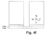
- Fig. 4f shows a subsequent processing step where orifice layer 318a is positioned over barrier layer 316a in a known manner.
- Fig. 5a illustrates an alternative production technique for producing an exemplary print head similar to that produced in Figs. 4a-4f.
- Production of an exemplary print head begins with substrate 300b which is prepared in a manner similar to that described above in relation to Fig. 4a.
- Various thin-film layers 314b are positioned over second surface 303b in a manner known in the art to form various electrical components.
- barrier layer 316b Positioned over thin-films 314b is barrier layer 316b.
- a protective layer or coating 402b is positioned over barrier layer 316b.
- Protective layer 402b is intended to physically protect the underlying layers during processing.
- a conductive material 414b in the form of conductive layer 502 is positioned over protective layer 402c.
- Conductive layer 502 can perform a function similar to conductive fluid 416 described above. Accordingly, conductive layer 502 can reduce the damage induced by the transferred laser energy beyond the laser machining region. By reducing the incidence of energy transfer outside the laser machining region, such as at breakthrough, damage to thin-films 314b can be reduced or eliminated.
- conductive layer 502 comprises a metal foil positioned over protective layer 402b.
- the foil is electrically coupled to a grounded probe 504.
- conductive fluid can be sprayed on protective layer 402b before conductive layer 502 is positioned thereon to decrease any resistance to electrical flow between the layers.
- Suitable conductive layers 502 can comprise a metal or otherwise conductive mesh. Still other conductive layers may not be conductive in a stand alone environment, but may perform satisfactorily in different embodiments. For example, a generally non-conductive porous material may be applied over protective layer 402b. Prior to laser machining, a conductive liquid may be sprayed on or otherwise supplied to the porous material to create a conductive layer during laser processing. While the embodiment shown utilizes a single conductive layer 502, other suitable embodiments may use multiple layers.
- Still other embodiments may utilize a conductive layer 502 comprising a gel.
- a hydrophilic material can be applied at a convenient time during processing and then ionized water can be supplied to the hydrophilic material prior to laser processing.
- Such an embodiment may allow the conductive liquid to be supplied during a convenient processing step and eliminate supplying the conductive liquid during laser processing.
- a laser beam, such as laser beam 404b can be directed at the first and/or second surfaces 302b, 303b to remove material in a known manner.
- conductive layer 502 can be removed.
- conductive layer 502 can be removed with the same process that removes underlying protective layer 402b.
- Fig. 6a shows another alternative embodiment similar to that described above in relation to Figs. 4a-4f.
- Fig. 6a shows a substrate processing device indicated generally at 602 and configured to laser machine substrate 300c.
- a means for generating optical energy configured to remove substrate material is embodied as laser source 604.
- Laser source 604 directs laser beam 404c toward first surface 302c from a direction sufficient to contact the first surface before contacting second surface 303c.
- a first fluid supply structure 606a supplies fluid in the form of water 608 toward first surface 302c and from a direction sufficient to contact the first surface before contacting second surface 303c.
- First fluid supply structure 606a supplies water 608 during laser processing primarily to aid in the substrate removal process.
- a second fluid supply structure 606b supplies conductive fluid 416c toward substrate 300c.
- second fluid supply structure 606b is configured to supply conductive fluid 416c in the form of ionized liquid water toward second surface 303c from a direction sufficient to contact second surface 303c before contacting first surface 302c.
- Second fluid supply structure 606b supplies conductive fluid 416c primarily to minimize damage to a layer assembly 307c positioned over second surface 303c and not primarily to aid in material removal.
- Figs. 7a-7d illustrate exemplary production techniques for dicing a wafer into individual integrated circuits.
- laser beam 404d is directed toward wafer 702 to separate or dice the wafer into separate and distinct subunits comprising integrated circuits 704a, 704b which comprise substrates 300d, 300e respectively.
- Laser beam 404d is specifically directed toward a street 706 upon which no thin-films 314d are formed and which separates individual integrated circuits comprising wafer 702.
- protective layer 402d was positioned over second surface 303d to protect the thin-films 314d during processing.
- Conductive liquid 416d is being supplied to portions of the protective layer 402d including the laser machining region 406d while laser beam 404d removes material from protective layer 402d.
- conductive fluid 416d is being supplied primarily to protect the thin-films 314d and not primarily to aid in the removal process such as by increasing the rate of removal achieved by the laser.
- laser beam 404d has passed through protective layer 402d and is removing substrate material comprising second surface 303d of the substrates 300d, 300e.
- Conductive fluid 416d is still being applied at this point in the processing to protect the thin-films from degradation.
- conductive fluid 416d is no longer being supplied at this point in the laser processing.
- Other embodiments may supply conductive fluid 416d for an entirety of laser machining operations.
- FIG. 7d shows the singulated integrated circuits 704a, 704b.
- Protective layer 402d can now be removed in a known manner.
- the laser machining process described in relation to Figs. 7a-7d allows wafers to be singulated into individual integrated circuits while minimizing damage to thin-films and/or other layers positioned upon the wafer during processing. Such a process can be especially valuable by allowing the laser removal process to be used in relative proximity to thin-film elements such as resistors and transistors without damaging those elements. As such some embodiments may allow streets to have a reduced width and save real estate on the wafer.
- the energy to be dissipated by the conductive material is a function of the laser energy provided and the properties of the material being ablated. Since the charge generated can be measured by applying a laser having the desired energy, e.g. pulse energy in the case of a pulse laser, and then measuring the charge concentration at one or more positions, e.g. by use of a charge probe, at locations that correspond to the location of components or areas where damage may occur. Based upon these measurements of charge concentration, ranges of conductivities for a conductive material may be determined that substantially reduce charge concentrations formed during laser ablation.
- a laser having the desired energy e.g. pulse energy in the case of a pulse laser
Landscapes
- Physics & Mathematics (AREA)
- Optics & Photonics (AREA)
- Engineering & Computer Science (AREA)
- Plasma & Fusion (AREA)
- Mechanical Engineering (AREA)
- Particle Formation And Scattering Control In Inkjet Printers (AREA)
Abstract
Description
- The market for electronic devices containing integrated circuits continually demands increased performance at decreased costs. To satisfy these demands various production techniques are employed to produce integrated circuits.
- Integrated circuits comprise a substrate over which other various layers are positioned to form the integrated circuit. Various substrate removal techniques can be utilized during processing. One production technique involves laser machining to selectively remove substrate material. Such laser machining can be useful in various production applications including forming slotted substrates configured for incorporation into various fluid-ejecting devices. Such fluid-ejecting devices can be adapted to various applications including print heads for ink jet print cartridges, as well as various other laboratory and medical applications.
- Laser machining can also be useful in other production applications, such as dicing of wafers into individual substrates. While laser machining is a useful production technique, present laser machining techniques can cause incidental damage to component layers positioned on a substrate during laser processing. Thus a need exists for improved laser processing technologies.
- The same components are used throughout the drawings to reference like features and components wherever feasible. Alphabetic suffixes are utilized to designate different embodiments. The illustrations described below are schematic representations of exemplary devices and methods of manufacture. It should be understood that the illustrations may not be to scale and certain dimensions may be exaggerated or reduced in the interests of clarity.
- Fig. 1 illustrates a front elevational view of a diagrammatic representation of an exemplary printer in accordance with one exemplary embodiment.
- Fig. 2 illustrates a perspective view of a diagrammatic representation of a print cartridge suitable for use in the exemplary printer shown in Fig. 1 in accordance with one exemplary embodiment.
- Fig. 3 illustrates a diagrammatic representation of a side-sectional view of a portion of the print cartridge shown in Fig. 2 in accordance with one exemplary embodiment.
- Figs. 4a-4f illustrate diagrammatic representations of process steps for laser processing an exemplary slotted substrate in accordance with one embodiment.
- Fig. 5a illustrates a diagrammatic representation of a process step for laser processing an exemplary slotted substrate in accordance with one embodiment.
- Fig. 6a illustrates a diagrammatic representation of a process step for laser processing an exemplary slotted substrate in accordance with one embodiment.
- Figs. 7a-7d illustrate diagrammatic representations of process steps for laser processing to separate individual substrates in accordance with one embodiment.
- The embodiments described below pertain to methods and systems for laser processing of integrated circuits. The integrated circuits comprise a substrate having various layers positioned thereon. Laser processing can be utilized to form a feature such as a slot, trench or other through or blind feature, within an individual integrated circuit. Alternatively or additionally, laser processing can be utilized to separate integrated circuits from one another. The embodiments described below allow the laser machining process to produce high quality substrates and associated layers.
- Fig. 1 illustrates a diagrammatic representation of an exemplary printing device that can utilize an exemplary print cartridge. In this embodiment, the printing device comprises a
printer 100. The printer shown here is embodied in the form of an inkjet printer. Theprinter 100 can be capable of printing in black-and-white and color. The term "printing device" refers to any type of printing device and/or image forming device that employs slotted substrate(s) to achieve at least a portion of its functionality. Examples of such printing devices can include, but are not limited to, printers, facsimile machines, and photocopiers. In this exemplary printing device, the slotted substrates comprise a portion of a print head which is incorporated into a print cartridge, an example of which is described below. - Fig. 2 shows a diagrammatic representation of an
exemplary print cartridge 202 that can be utilized in an exemplary printing device. The print cartridge is comprised of aprint head 204 and acartridge body 206 that supports the print head.Print head 204 comprises an example of an integrated circuit in the form of a fluid-ejecting device. Though asingle print head 204 is employed on thisprint cartridge 202 other exemplary configurations may employ multiple print heads on a single cartridge. -
Print cartridge 202 is configured to have a self-contained fluid or ink supply withincartridge body 206. Other print cartridge configurations may alternatively or additionally be configured to receive fluid from an external supply. Other exemplary configurations will be recognized by those of skill in the art. - Reliability of
print cartridge 202 is desirable for proper functioning ofprinter 100. Further, failure of print cartridges and/or defective print cartridges increases production costs. Print cartridge failure can be brought about by defective or faulty print cartridge components. Such component failure can be caused by among other factors damage to print cartridge components during manufacture. As such, various embodiments described below can provide print heads with a reduced propensity for failure. - Fig. 3 shows a cross-sectional diagrammatic representation of a portion of the
exemplary print head 204, taken along line 3-3 in Fig. 2. Here, asubstrate 300 extends between a first substrate surface ("first surface") 302 and a second substrate surface ("second surface") 303 to define a thickness t there between. Aslot 305 passes throughsubstrate 300 between first andsecond surfaces slot 305. In this embodiment the x-axis comprises a long axis extending into and out of the plane of the page upon which Fig. 3 appears. - In one embodiment,
substrate 300 comprises silicon which can be either doped or undoped. Other suitable substrate materials can include, but are not limited to, gallium arsenide, gallium phosphide, indium phosphide, glass or other material. - Substrate thicknesses t can have any suitable dimensions that are appropriate for substrates' intended applications. In some embodiments, substrate thicknesses taken relative to the z-direction can range from less than 100 microns to more than 2000 microns. One exemplary embodiment can utilize a substrate that is approximately 675 microns thick. Though a single substrate is discussed herein, other suitable embodiments may comprise a substrate that has multiple components during assembly and/or in the finished product. For example, one such embodiment may employ a substrate having a first component and a second sacrificial component which is discarded at some point during processing.
- A
layer assembly 307 comprising one or more layers is formed over thesecond surface 303 of the substrate. In some embodiments,layer assembly 307 comprises afirst sub-assembly 311 of one or more layers, and asecond sub-assembly 312 of one or more layers. In this particular example,first sub-assembly 311 comprises one or more thin-film layers 314, andsecond sub-assembly 312 comprises one or more thick-film layers, which in one embodiment comprise a photo-imagable polymer. Other suitable examples are provided below. In at least one embodiment, thesecond sub-assembly 312 comprises abarrier layer 316 and an orifice plate ororifice layer 318. - In one embodiment, one or more thin-
film layers 314 can be patterned to comprise one or more electrical components such as electrical traces (not specifically shown)resistors 320 and transistors (not specifically shown). Individual resistors can be selectively controlled via the electrical traces. Thin-film layers 314 can in some embodiments also define, at least in part, a wall or surface of multiple fluid-feed passageways 322 through which fluid can pass.Barrier layer 316 can define, at least in part, multiple firingchambers 324. In some embodiments,barrier layer 316 may, in combination with thin-film layers 314, define fluid-feed passageways 322.Orifice layer 318 can definemultiple firing nozzles 326. Individual firing nozzles can be respectively aligned withindividual firing chambers 324. -
Barrier layer 316 andorifice layer 318 can be formed in any suitable manner. In one embodiment, bothbarrier layer 316 andorifice layer 318 comprise thick-film material, such as a photo-imagable polymer material. The photo-imagable polymer - material can be applied in any suitable manner. For example, the material can be "spun-on" as will be recognized by the skilled artisan.
- After being spun-on,
barrier layer 316 can then be patterned to form, at least in part, desired features, such as firingchambers 324, therein. In one embodiment, patterned areas of the barrier layer can be filled with a sacrificial material. In this embodiment,orifice layer 318 can be comprised of the same material as the barrier layer and be formed overbarrier layer 316. In one such example, orifice layer material is 'spun-on' over the barrier layer.Orifice layer 318 can then be patterned as desired to formnozzles 326 overrespective chambers 324. The sacrificial material is then removed from the barrier layer'schambers 324 andpassageways 322. - In another embodiment,
barrier layer 316 comprises a thick-film, while theorifice layer 318 comprises an electroformed nickel material. Other suitable embodiments may employ an orifice layer which performs the functions of both a barrier layer and an orifice layer. - In operation, fluid such as ink can enter
slot 305 from the cartridge body, shown Fig. 2. Fluid can then flow throughindividual passageways 322 into anindividual chamber 324. Fluid can be ejected from the chamber when an electrical current is passed through anindividual resistor 320. The electrical current can heat the resistor sufficiently to vaporize some of the fluid contained in the firing chamber so that it expands to eject a portion of the remaining fluid from a respectively positionednozzle 326. The ejected fluid can then be replaced by additional fluid frompassageway 322. - Figs. 4a-4f illustrate production techniques for producing an exemplary print head similar to
print head 204 shown in Fig. 3. The skilled artisan should recognize that the production techniques described below are equally applicable to other types of fluid-ejecting devices or other microelectronic devices in which features are formed. - Referring to Fig. 4a, fabrication of an exemplary print head begins with a
substrate 300a. Various characteristics of the substrate are described above. Various thin-film layers 314a are positioned oversecond surface 303a in a manner known in the art to form various electrical components. In some embodiments, the thin-film layers 314a comprise at least one patterned conductive layer and at least one dielectric layer. In other embodiments thin-film layers 314a may include anti-cavitation and/or other protective layers as are known in the art. - Positioned over thin-
films 314a isbarrier layer 316a. The barrier layer may be patterned at this point to form the various firing chambers described above in relation to Fig. 3. Alternatively, the firing chambers may be formed at a subsequent point in the processing. - In one embodiment, one or more protective layer(s) or coating(s) 402 is positioned over
barrier layer 316a.Protective layer 402 is intended to physically protect the underlying layers during laser processing. Among other functions,protective layer 402 can protect the underlying layers from debris produced during laser machining. Withoutprotective layer 402, such debris can become trapped in the underlying layers and cause fluidic and/or electrical failure. For example withoutprotective layer 402, debris produced during laser processing can become lodged in the fluid-feed passageways 322 as described in Fig. 3. The debris can subsequently occlude or obstruct ink flow through the affected passageways resulting in a malfunction during printing. Suitable protective layer materials can be applied before laser processing and removed after laser processing. - Suitable protective layer materials can include various polymers such as thermoplastics and cross-linking polymers among others. In one embodiment,
protective layer 402 comprises polyvinyl alcohol. Other suitable materials for protective layers can include but are not limited to polyvinyl acetate, polyethylene oxide, and polyethyleneterathalate, among others. - Processing techniques which utilize optical alignment equipment can utilize materials such as polyvinyl alcohol which allow sufficient optical transmission for the equipment to operate. For example, where optical alignment equipment is utilized to locate fiducial markings on the print head the protective layer should allow sufficient light transmission for proper equipment functioning.
-
Protective layer 402 can be formed from a polyvinyl alcohol water solution that is commercially available from ATMI. The solution can be applied and then dried before laser processing. Upon completion of laser processing pressurized water and/or mechanical means such as brushing in the presence of water can be utilized to remove the protective layer.Protective layer 402 can be applied utilizing any suitable technique. In one embodimentprotective layer 402 is spun-on. Other suitable embodiments may apply the protective layer by laminating, dip coating, electrocoating, sputter coating or spray coating, among other processes. In one embodiment, thin-films 314a,barrier layer 318a andprotective layer 402 compriselayer assembly 307a. - A
laser beam 404 is directed atsubstrate 300a. Any suitable laser beam configured to remove substrate material can be utilized.Laser beam 404 is directed through the substrate'sfirst surface 302a from a direction sufficient to contactfirst surface 302a before contacting thesecond surface 303a.Laser beam 404 is directed at alaser machining region 406 of substrate material and the laser energy removes substrate material so thatlaser machining region 406 progressively moves towardsecond surface 303a. The removed substrate material defines afeature 408 having a generally uniform width w throughout its depth d as defined betweensidewalls - In some implantations
laser machining region 406 can be defined laterally as extending betweensidewalls laser machining region 406 can include substratematerial defining sidewalls - Referring now to Figs. 4b-4c where
laser beam 404 approaches "break-through" ofsecond surface 303a. Fig. 4c illustrates an enlarged region of the substrate illustrated in Fig. 4b. As shown in Figs. 4b-4c,laser machining region 406 now comprises substrate material definingsecond surface 303a and portions oflayer assembly 307a. At this point in the laser machining process, with previous technologies, laser energy directed atlaser machining region 406 may unintentionally be transferred to substrate material and/orlayer assembly 307a outside oflaser machining region 406. Such energy transfer can damage thin-film layers 314a among others. Such energy transfer can damage regions of the thin-films or other components of thelayer assembly 307 that are located from about 10 microns to about 125 microns away from the laser machining region. Thus, some of the unintended energy transfer can damage portions of thelayer assembly 307a at locations an order of magnitude beyond the heat affected zone. - The described embodiments reduce or eliminate damage caused by unintended energy transfer by supplying an electrically
conductive material 414 proximatesecond surface 303a during at least a portion of the laser machining process. Suitable electricallyconductive materials 414 can include fluids and solids among others. Several exemplary materials and methods of use are described below.
As illustrated in Figs. 4b-4c the present embodiment reduces or eliminates damage to thelayer assembly 307 by supplying an electricallyconductive material 414 comprisingfluid 416. The fluid is directed towardsecond surface 303a.Fluid 416 can itself be conductive and/or can contain material(s) which makes the fluid conductive. In this embodiment, the fluid comprises ionized water having a conductivity of about 100 micro Siemens per centimeter and delivered as atomized water droplets. The ionized water is delivered at a rate of about 8 milliliters/minute. - Many other
suitable fluids 416 can be utilized in various embodiments. In one such example, a highly viscous and/or tacky liquid may be utilized which will may adhere to the layer assembly for a prolonged period of time during processing and as such may be supplied periodically rather than generally continuously during laser processing. Other suitable conductive fluids can comprise gases having sufficient rates of conductivity. For example, some embodiments may utilize supersaturated gases or vapors as the conductive fluid. - Any suitable delivery mechanism can be utilized to supply
conductive fluid 416. In one embodimentconductive fluid 416 is supplied from anatomizing nozzle 418 and from a direction sufficient to contactfirst surface 302a before contacting thesecond surface 303a. - Various other types of delivery means can be utilized to supply
conductive fluid 416. For example, in one embodiment,conductive fluid 416 flows across at least portions oflayer assembly 307a. Another embodiment immerses portions of thesubstrate 300a andlayer assembly 307a inconductive fluid 416. In addition to atomizingnozzle 418, other suitable nozzle means can be utilized to direct the conductive fluid towardsecond surface 303a. - Several mechanisms have been proposed to explain the damage associated with previous laser machining technologies, and other explanations may be forthcoming. One explanation proposes that at break-through of
second surface 303a,laser beam 404 creates localized electrostatic charges onlayer assembly 307a outside oflaser machining region 406. The electrostatic charges are unable to sufficiently dissipate and as a result accumulate until sudden catastrophic electrostatic discharges ensue within the layer assembly. The catastrophic electrostatic discharges can have an intensity sufficient to damage some of the component layers such as the thin-films, e.g. by causing breakdown of dielectric layers formed between conductive layers. Supplying the conductive material to layerassembly 307a allows charges to dissipate as they are generated and thus reduces the likelihood of catastrophic electrostatic discharges and other problems caused by excessive charge accumulation. - Experimental evidence indicates that damage to
layer assembly 307a outside oflaser machining region 406 can be reduced or eliminated by supplyingconductive material 414 tolayer assembly 307a during at least a portion, e.g. whenlaser beam 404 is approximately half way through thickness t ofsubstrate 300a, of the laser machining process. In other embodiments, the conductive material can be supplied during a period associated with breakthrough of a substrate surface over which the layer assembly is positioned. In additional embodiments, conductive material can be supplied prior to and during the application oflaser beam 404. - Referring now to Fig. 4d which shows
laser beam 404 nearing completion of the laser machining process.Laser beam 404 is removing material fromlayer assembly 307a in the process of formingfeature 408. - Fig. 4e shows the resultant substrate upon completion of the laser machining process. Feature 408 as described above, now passes through the
entire substrate 300a, thin-films 314a andbarrier layer 316a and as such now comprisesslot 305a.Protective layer 402 described above has been removed subsequent to laser processing by known techniques. - Referring now to Fig. 4f which shows a subsequent processing step where
orifice layer 318a is positioned overbarrier layer 316a in a known manner. - Fig. 5a illustrates an alternative production technique for producing an exemplary print head similar to that produced in Figs. 4a-4f. Production of an exemplary print head begins with
substrate 300b which is prepared in a manner similar to that described above in relation to Fig. 4a. Various thin-film layers 314b are positioned oversecond surface 303b in a manner known in the art to form various electrical components. Positioned over thin-films 314b isbarrier layer 316b. A protective layer orcoating 402b is positioned overbarrier layer 316b.Protective layer 402b is intended to physically protect the underlying layers during processing. - A
conductive material 414b in the form ofconductive layer 502 is positioned over protective layer 402c.Conductive layer 502 can perform a function similar toconductive fluid 416 described above. Accordingly,conductive layer 502 can reduce the damage induced by the transferred laser energy beyond the laser machining region. By reducing the incidence of energy transfer outside the laser machining region, such as at breakthrough, damage to thin-films 314b can be reduced or eliminated. - In one embodiment,
conductive layer 502 comprises a metal foil positioned overprotective layer 402b. In one embodiment, the foil is electrically coupled to a groundedprobe 504. Also, in this embodiment, conductive fluid can be sprayed onprotective layer 402b beforeconductive layer 502 is positioned thereon to decrease any resistance to electrical flow between the layers. - Other suitable
conductive layers 502 can comprise a metal or otherwise conductive mesh. Still other conductive layers may not be conductive in a stand alone environment, but may perform satisfactorily in different embodiments. For example, a generally non-conductive porous material may be applied overprotective layer 402b. Prior to laser machining, a conductive liquid may be sprayed on or otherwise supplied to the porous material to create a conductive layer during laser processing. While the embodiment shown utilizes a singleconductive layer 502, other suitable embodiments may use multiple layers. - Still other embodiments may utilize a
conductive layer 502 comprising a gel. In one such embodiment, a hydrophilic material can be applied at a convenient time during processing and then ionized water can be supplied to the hydrophilic material prior to laser processing. Such an embodiment may allow the conductive liquid to be supplied during a convenient processing step and eliminate supplying the conductive liquid during laser processing. - A laser beam, such as
laser beam 404b can be directed at the first and/orsecond surfaces conductive layer 502 can be removed. In some embodiments,conductive layer 502 can be removed with the same process that removes underlyingprotective layer 402b. - Referring now to which Fig. 6a which shows another alternative embodiment similar to that described above in relation to Figs. 4a-4f. Fig. 6a shows a substrate processing device indicated generally at 602 and configured to
laser machine substrate 300c. A means for generating optical energy configured to remove substrate material is embodied aslaser source 604. -
Laser source 604 directslaser beam 404c towardfirst surface 302c from a direction sufficient to contact the first surface before contactingsecond surface 303c. A firstfluid supply structure 606a supplies fluid in the form ofwater 608 towardfirst surface 302c and from a direction sufficient to contact the first surface before contactingsecond surface 303c. Firstfluid supply structure 606a supplieswater 608 during laser processing primarily to aid in the substrate removal process. - A second
fluid supply structure 606b suppliesconductive fluid 416c towardsubstrate 300c. In this instance secondfluid supply structure 606b is configured to supplyconductive fluid 416c in the form of ionized liquid water towardsecond surface 303c from a direction sufficient to contactsecond surface 303c before contactingfirst surface 302c. Secondfluid supply structure 606b suppliesconductive fluid 416c primarily to minimize damage to a layer assembly 307c positioned oversecond surface 303c and not primarily to aid in material removal. - The reader is now directed to Figs. 7a-7d which illustrate exemplary production techniques for dicing a wafer into individual integrated circuits.
- Referring now to Fig. 7a,
laser beam 404d is directed towardwafer 702 to separate or dice the wafer into separate and distinct subunits comprisingintegrated circuits substrates Laser beam 404d is specifically directed toward astreet 706 upon which no thin-films 314d are formed and which separates individual integratedcircuits comprising wafer 702. In a prior process stepprotective layer 402d was positioned oversecond surface 303d to protect the thin-films 314d during processing. -
Conductive liquid 416d is being supplied to portions of theprotective layer 402d including the laser machining region 406d whilelaser beam 404d removes material fromprotective layer 402d. In this instance,conductive fluid 416d is being supplied primarily to protect the thin-films 314d and not primarily to aid in the removal process such as by increasing the rate of removal achieved by the laser. - Referring now to Fig. 7b,
laser beam 404d has passed throughprotective layer 402d and is removing substrate material comprisingsecond surface 303d of thesubstrates Conductive fluid 416d is still being applied at this point in the processing to protect the thin-films from degradation. - Referring now to Fig. 7c where
laser beam 404d is continuing to remove substrate material and is now proximate tofirst surface 302d. In one embodiment,conductive fluid 416d is no longer being supplied at this point in the laser processing. Other embodiments may supplyconductive fluid 416d for an entirety of laser machining operations. - Referring now to Fig. 7d which shows the singulated
integrated circuits Protective layer 402d can now be removed in a known manner. - The laser machining process described in relation to Figs. 7a-7d allows wafers to be singulated into individual integrated circuits while minimizing damage to thin-films and/or other layers positioned upon the wafer during processing. Such a process can be especially valuable by allowing the laser removal process to be used in relative proximity to thin-film elements such as resistors and transistors without damaging those elements. As such some embodiments may allow streets to have a reduced width and save real estate on the wafer.
- It should be noted that the energy to be dissipated by the conductive material is a function of the laser energy provided and the properties of the material being ablated. Since the charge generated can be measured by applying a laser having the desired energy, e.g. pulse energy in the case of a pulse laser, and then measuring the charge concentration at one or more positions, e.g. by use of a charge probe, at locations that correspond to the location of components or areas where damage may occur. Based upon these measurements of charge concentration, ranges of conductivities for a conductive material may be determined that substantially reduce charge concentrations formed during laser ablation.
- Although specific structural features and methodological steps are described, it is to be understood that the inventive concepts defined in the appended claims are not necessarily limited to the specific features or steps described. Rather, the specific features and steps are disclosed as forms of embodiments of the inventive concepts.
Claims (15)
- A method comprising:removing substrate material between a first substrate surface and a second generally opposing substrate surface by directing a laser beam at the first substrate surface; and,during at least a portion of said removing, supplying a conductive liquid proximate a second surface of the substrate.
- The method of claim 1, further comprising a layer assembly positioned over the second surface and wherein supplying the conductive liquid comprises supplying the conductive fluid proximate the layer assembly.
- The method of claim 1 or 2, wherein said act of supplying comprises directing liquid droplets toward the second surface.
- The method of any preceding claim, wherein the act of supplying occurs at least when the optical energy removes substrate material defining the second surface.
- The method of claim 1, wherein the act of supplying comprises supplying the electrically conductive fluid to a layer assembly positioned over the second surface and wherein the layer assembly comprises at least one electrically conductive layer and at least one dielectric layer.
- A method comprising:forming a feature into a substrate, at least in part, by directing a laser beam at the substrate; and,during at least a portion of said directing, supplying a conductive liquid proximate the substrate primarily to protect portions of a layer assembly positioned over the substrate and not primarily to aid in forming the feature.
- The method of claim 6, wherein said act of supplying protects the portion of the layer assembly that is not contained with a laser machining region which the laser is directed toward.
- The method of claim 6, wherein said act of supplying protects the portion of the layer assembly by dissipating electrostatic charges from localized areas of the layer assembly.
- The method of claim 6, wherein said act of supplying decreases an incidence of laser energy being unintentionally transferred to portions of the layer assembly distal the feature.
- The method of any of claims 6 to 9, wherein said act of forming comprises first directing the laser beam at substrate material proximate a first substrate surface and second directing the laser beam at substrate material intermediate the first surface and a second surface and third directing the laser beam at substrate material proximate the second substrate surface and wherein the layer assembly is positioned over the second surface.
- The method of claim 10, wherein said act of supplying comprises supplying the conductive liquid proximate the first surface of the substrate.
- The method of claim 10, wherein said act of supplying comprises supplying the conductive liquid proximate the second surface of the substrate.
- The method of claim 6, wherein said act of supplying comprises supplying the conductive liquid proximate the first surface of the substrate and the second first surface of the substrate.
- The method of any of claims 6 to 13, wherein said act of supplying comprises supplying ionized water.
- The method of any of claims 6 to 13, wherein said act of supplying comprises supplying a gelatinous liquid.
Applications Claiming Priority (2)
| Application Number | Priority Date | Filing Date | Title |
|---|---|---|---|
| US10/850,732 US7163640B2 (en) | 2004-05-21 | 2004-05-21 | Methods and systems for laser processing |
| US850732 | 2004-05-21 |
Publications (1)
| Publication Number | Publication Date |
|---|---|
| EP1598141A1 true EP1598141A1 (en) | 2005-11-23 |
Family
ID=34941286
Family Applications (1)
| Application Number | Title | Priority Date | Filing Date |
|---|---|---|---|
| EP05252943A Withdrawn EP1598141A1 (en) | 2004-05-21 | 2005-05-12 | Methods for laser processing |
Country Status (2)
| Country | Link |
|---|---|
| US (2) | US7163640B2 (en) |
| EP (1) | EP1598141A1 (en) |
Families Citing this family (5)
| Publication number | Priority date | Publication date | Assignee | Title |
|---|---|---|---|---|
| US7163640B2 (en) * | 2004-05-21 | 2007-01-16 | Hewlett-Packard Development Company, L.P. | Methods and systems for laser processing |
| US7938974B2 (en) * | 2007-03-12 | 2011-05-10 | Silverbrook Research Pty Ltd | Method of fabricating printhead using metal film for protecting hydrophobic ink ejection face |
| US7605009B2 (en) * | 2007-03-12 | 2009-10-20 | Silverbrook Research Pty Ltd | Method of fabrication MEMS integrated circuits |
| JP5427852B2 (en) * | 2011-08-23 | 2014-02-26 | 東芝テック株式会社 | Inkjet head manufacturing method and inkjet head |
| EP3446111B1 (en) | 2016-08-03 | 2022-03-09 | Hewlett-Packard Development Company, L.P. | Conductive wire disposed in a layer |
Citations (6)
| Publication number | Priority date | Publication date | Assignee | Title |
|---|---|---|---|---|
| US4766009A (en) * | 1984-07-23 | 1988-08-23 | Hitachi, Ltd. | Selective working method |
| WO1989003274A1 (en) * | 1987-10-14 | 1989-04-20 | Akademiet For De Tekniske Videnskaber, Svejsecentr | Method and application of laser drilling |
| DE3937460A1 (en) * | 1989-11-10 | 1990-11-08 | Daimler Benz Ag | METHOD FOR ATTACHING RESIDUE-FREE BREAK-FREE HOLES INTO THE WALL OF A FLUID PIPE |
| DE19856346A1 (en) * | 1998-12-07 | 2000-06-15 | Schott Spezialglas Gmbh | Apparatus for cutting workpiece from brittle material has liquid bath cooling arrangement in which workpiece is arranged in suitable liquid with gas source for generating directed gas flow |
| EP1293316A1 (en) * | 2001-08-28 | 2003-03-19 | Tokyo Seimitsu Co.,Ltd. | Dicing method and apparatus |
| EP1533069A1 (en) * | 2003-11-14 | 2005-05-25 | Hewlett-Packard Development Company, L.P. | Laser micromachining and methods of same |
Family Cites Families (9)
| Publication number | Priority date | Publication date | Assignee | Title |
|---|---|---|---|---|
| US4437109A (en) * | 1980-11-07 | 1984-03-13 | General Electric Company | Silicon-on-sapphire body with conductive paths therethrough |
| US5468652A (en) * | 1993-07-14 | 1995-11-21 | Sandia Corporation | Method of making a back contacted solar cell |
| US5543365A (en) * | 1994-12-02 | 1996-08-06 | Texas Instruments Incorporated | Wafer scribe technique using laser by forming polysilicon |
| JP3506002B2 (en) * | 1997-07-28 | 2004-03-15 | 松下電工株式会社 | Manufacturing method of printed wiring board |
| US6392683B1 (en) * | 1997-09-26 | 2002-05-21 | Sumitomo Heavy Industries, Ltd. | Method for making marks in a transparent material by using a laser |
| US6727593B2 (en) * | 2001-03-01 | 2004-04-27 | Kabushiki Kaisha Toshiba | Semiconductor device with improved bonding |
| US6527368B1 (en) * | 2002-04-30 | 2003-03-04 | Hewlett-Packard Company | Layer with discontinuity over fluid slot |
| JP2004193399A (en) * | 2002-12-12 | 2004-07-08 | Denso Corp | Semiconductor device and manufacturing method thereof |
| US7163640B2 (en) * | 2004-05-21 | 2007-01-16 | Hewlett-Packard Development Company, L.P. | Methods and systems for laser processing |
-
2004
- 2004-05-21 US US10/850,732 patent/US7163640B2/en not_active Expired - Fee Related
-
2005
- 2005-05-12 EP EP05252943A patent/EP1598141A1/en not_active Withdrawn
-
2006
- 2006-12-04 US US11/566,586 patent/US7938512B2/en not_active Expired - Fee Related
Patent Citations (6)
| Publication number | Priority date | Publication date | Assignee | Title |
|---|---|---|---|---|
| US4766009A (en) * | 1984-07-23 | 1988-08-23 | Hitachi, Ltd. | Selective working method |
| WO1989003274A1 (en) * | 1987-10-14 | 1989-04-20 | Akademiet For De Tekniske Videnskaber, Svejsecentr | Method and application of laser drilling |
| DE3937460A1 (en) * | 1989-11-10 | 1990-11-08 | Daimler Benz Ag | METHOD FOR ATTACHING RESIDUE-FREE BREAK-FREE HOLES INTO THE WALL OF A FLUID PIPE |
| DE19856346A1 (en) * | 1998-12-07 | 2000-06-15 | Schott Spezialglas Gmbh | Apparatus for cutting workpiece from brittle material has liquid bath cooling arrangement in which workpiece is arranged in suitable liquid with gas source for generating directed gas flow |
| EP1293316A1 (en) * | 2001-08-28 | 2003-03-19 | Tokyo Seimitsu Co.,Ltd. | Dicing method and apparatus |
| EP1533069A1 (en) * | 2003-11-14 | 2005-05-25 | Hewlett-Packard Development Company, L.P. | Laser micromachining and methods of same |
Also Published As
| Publication number | Publication date |
|---|---|
| US7163640B2 (en) | 2007-01-16 |
| US20070090088A1 (en) | 2007-04-26 |
| US20050260778A1 (en) | 2005-11-24 |
| US7938512B2 (en) | 2011-05-10 |
Similar Documents
| Publication | Publication Date | Title |
|---|---|---|
| JP2005523833A (en) | Apparatus and method for characterizing a surface | |
| JPH11204529A (en) | Pattern forming method and substrate manufacturing apparatus | |
| KR101099952B1 (en) | Micro Devices, Print Heads, and Fluid Dispensing Devices | |
| EP1598141A1 (en) | Methods for laser processing | |
| JPH06297719A (en) | Liquid droplet jet device and production thereof | |
| US7893386B2 (en) | Laser micromachining and methods of same | |
| JP2009061614A (en) | Ink jet head and method of manufacturing ink jet head | |
| EP0495649A1 (en) | Method for manufacturing an ink jet recording head | |
| US7923658B2 (en) | Laser micromachining methods and systems | |
| CN1860029A (en) | Methods and systems for conditioning slotted substrates | |
| JP4393730B2 (en) | Inkjet head | |
| US7441868B2 (en) | Nozzle plate and method of manufacturing the same | |
| CN1926056B (en) | Slot forming method and fluid ejection mechanism | |
| CN101508202B (en) | Liquid ejection head and manufacturing method thereof | |
| CN101052495A (en) | Laser micromachining methods and systems using a liquid as an assist medium | |
| US6515255B1 (en) | Processing method of discharge nozzle for liquid jet recording head and manufacturing method of liquid jet recording head | |
| EP1693204A2 (en) | Liquid droplet jetting apparatus and nozzle plate used in the same | |
| JPH05330061A (en) | Production of liquid droplet jet device | |
| JP2001130000A (en) | Ink-jet recording head and ink-jet recording apparatus | |
| JP2006130701A (en) | Ink ejection device | |
| JP2001150678A (en) | Ink-jet recording head | |
| CN115195292A (en) | Ink jetting device with various jetting methods | |
| JP6609977B2 (en) | NOZZLE PLATE, INKJET HEAD, INKJET DEVICE, AND NOZZLE PLATE MANUFACTURING METHOD | |
| JP2007130816A (en) | Droplet discharge head, manufacturing method thereof, and ink jet recording apparatus | |
| US20060113285A1 (en) | Methods of laser ablating polymeric materials to provide uniform laser ablated features therein |
Legal Events
| Date | Code | Title | Description |
|---|---|---|---|
| PUAI | Public reference made under article 153(3) epc to a published international application that has entered the european phase |
Free format text: ORIGINAL CODE: 0009012 |
|
| AK | Designated contracting states |
Kind code of ref document: A1 Designated state(s): AT BE BG CH CY CZ DE DK EE ES FI FR GB GR HU IE IS IT LI LT LU MC NL PL PT RO SE SI SK TR |
|
| AX | Request for extension of the european patent |
Extension state: AL BA HR LV MK YU |
|
| 17P | Request for examination filed |
Effective date: 20060213 |
|
| AKX | Designation fees paid |
Designated state(s): CH DE GB LI |
|
| 17Q | First examination report despatched |
Effective date: 20091006 |
|
| GRAP | Despatch of communication of intention to grant a patent |
Free format text: ORIGINAL CODE: EPIDOSNIGR1 |
|
| STAA | Information on the status of an ep patent application or granted ep patent |
Free format text: STATUS: THE APPLICATION IS DEEMED TO BE WITHDRAWN |
|
| 18D | Application deemed to be withdrawn |
Effective date: 20101109 |