EP1596468A2 - Filters - Google Patents
Filters Download PDFInfo
- Publication number
- EP1596468A2 EP1596468A2 EP05270013A EP05270013A EP1596468A2 EP 1596468 A2 EP1596468 A2 EP 1596468A2 EP 05270013 A EP05270013 A EP 05270013A EP 05270013 A EP05270013 A EP 05270013A EP 1596468 A2 EP1596468 A2 EP 1596468A2
- Authority
- EP
- European Patent Office
- Prior art keywords
- filter
- antenna
- apodising
- array
- signal
- Prior art date
- Legal status (The legal status is an assumption and is not a legal conclusion. Google has not performed a legal analysis and makes no representation as to the accuracy of the status listed.)
- Withdrawn
Links
Images





Classifications
-
- H—ELECTRICITY
- H01—ELECTRIC ELEMENTS
- H01Q—ANTENNAS, i.e. RADIO AERIALS
- H01Q3/00—Arrangements for changing or varying the orientation or the shape of the directional pattern of the waves radiated from an antenna or antenna system
- H01Q3/26—Arrangements for changing or varying the orientation or the shape of the directional pattern of the waves radiated from an antenna or antenna system varying the relative phase or relative amplitude of energisation between two or more active radiating elements; varying the distribution of energy across a radiating aperture
- H01Q3/2676—Optically controlled phased array
-
- H—ELECTRICITY
- H01—ELECTRIC ELEMENTS
- H01Q—ANTENNAS, i.e. RADIO AERIALS
- H01Q21/00—Antenna arrays or systems
- H01Q21/06—Arrays of individually energised antenna units similarly polarised and spaced apart
- H01Q21/22—Antenna units of the array energised non-uniformly in amplitude or phase, e.g. tapered array or binomial array
-
- H—ELECTRICITY
- H01—ELECTRIC ELEMENTS
- H01Q—ANTENNAS, i.e. RADIO AERIALS
- H01Q3/00—Arrangements for changing or varying the orientation or the shape of the directional pattern of the waves radiated from an antenna or antenna system
- H01Q3/22—Arrangements for changing or varying the orientation or the shape of the directional pattern of the waves radiated from an antenna or antenna system varying the orientation in accordance with variation of frequency of radiated wave
Definitions
- the present invention relates to filters, and is more particularly concerned with apodising filters.
- Apodisation is often used in the optical domain to modify transmission properties of an aperture to suppress unwanted optical aberrations or effects.
- apodisation can also be applied to other regions within the electromagnetic spectrum, for example, the microwave frequency range.
- apodisation at microwave frequencies is in phased antenna arrays used in spatial discriminator systems for determining angles of arrival of incoming signals.
- a beam is generated by maintaining a fixed phase difference between elements of the antenna array.
- the shape of the beam which is generated from the antenna array is dependent on:
- the antenna array comprises closely spaced elements, it behaves as if it is a continuous aperture.
- the pattern beamwidth is inversely proportional to the frequency. This means that as the frequency increases, the pattern beamwidth becomes narrower. This is undesirable for wide bandwidth spatial discriminator systems for determining the angle of arrival of an incoming signal by examining the relative beam output levels.
- a method of controlling beam shape in a phased antenna array comprising the steps of:-
- the apodising may be carried out in the microwave domain or, altematively, in the optical domain if the signals from the antenna array are converted from electrical signals to optical signals.
- a method of controlling beam shape in a phased array antenna comprising the steps of:
- a filter arrangement including at least one apodising filter that provides a frequency-dependent taper on an aperture distribution.
- a filter arrangement for controlling beam shape in a phased array antenna comprising a number of antenna elements to receive a signal in a first frequency range
- the apodising filter system comprises a number of channels, wherein one of the number of channels is associated with one of the number of antenna elements and comprises:
- a spatial discriminator including a filter arrangement as described above.
- the error associated with the estimated angle of arrival is substantially smaller than an individual beamwidth.
- the beam crossover levels, and hence beamwidths must remain approximately constant over the bandwidth of interest.
- the pattern sidelobe levels must also remain sufficiently constant over the bandwidth. It is important to maintain the same beam shape across the bandwidth of a spatial discriminator so that the power needed to deconvolve the signal is much reduced. To accomplish this, frequency-dependent apodisation is used.
- microwave frequency filters are used at the antenna array. This means that more components need to be provided in the region of the antenna array. However, when space is a premium, this provides many disadvantages. Furthermore, computer simulations show that the tolerance on the power for each element varies from 0.5 dB to 1 dB in order to maintain the beam shape. This is extremely difficult to achieve using conventional filtering techniques.
- a spatial discriminator 100 comprises an antenna system as shown in Figure 1.
- the spatial discriminator 100 comprises an antenna array 102 consisting a plurality of antenna elements 102a, 102b, 102c, 102d, 102e, 102f, 102g, 102h.
- the antenna array 102 is a phased antenna array and each antenna element 102a, 102b, 102c, 102d, 102e, 102f, 102g, 102h has a fixed phase difference relative to each other antenna element.
- the antenna array 102 is connected to an array 104 of apodising filters.
- Each antenna element 102a, 102b, 102c, 102d, 102e, 102f, 102g, 102h is connected to a respective apodising filter element 104a, 104b, 104c, 104d, 104e, 104f, 104g, 104h - only filter elements 104a and 104h are labelled for clarity.
- the array 104 of apodising filters is connected to a beamforming unit 106 having four output ports 106j, 106k, 1061, 106m. Each output port 106j, 106k, 106l, 106m provides an output signal 108w, 108x, 108y, 108z.
- Each output signal 108w, 108x, 108y, 108z comprises a combination of the signals output from the antenna elements 102a, 102b, 102c, 102d, 102e, 102f, 102g, 102h through the respective apodising filter elements 104a, 104b, 104c, 104d, 104e, 104f, 104g, 104h.
- This is indicated by solid lines 106p and dotted lines 106q connecting apodising filter elements 104a, 104b, 104c, 104d, 104e, 104f, 104g, 104h to respective output ports 106j, 106k.
- the filter elements 104a, 104b, 104c, 104d, 104e, 104f, 104g, 104h are designed to apply a frequency-dependent amplitude across the aperture of the antenna array 102 as shown in Figure 2.
- Figure 2 illustrates the different intensity distributions according to the frequency of the received radiation.
- the intensities from each of the antenna elements in the antenna array 102 ( Figure 1), after filtering, are shown by dots 1202, 1204, 1206, 1208, 1210, 1212, 1214, 1216 and the distribution of these intensities across the array 102 is indicated by profiles 1220, 1230.
- Profile 1220 corresponds to a high frequency apodising intensity distribution
- profile 1230 corresponds to a low frequency apodising intensity distribution.
- the distribution is flatter at low frequencies than at high frequencies.
- the outer antenna elements are almost completely filtered out, so that the aperture is smaller.
- the aperture is larger.
- the effective aperture, measured in terms of wavelengths, however, remains constant, and the beamshape is the same at both high and low frequencies.
- the characteristics of the apodising filter elements 104a, 104b, 104c, 104d, 104e, 104f, 104g, 104h are therefore chosen so that the effective aperture size remains approximately constant irrespective of frequency.
- the required characteristics for some of the filters are shown in Figure 3.
- Filters 104c and 104f are required to have the characteristic 32 shown in Figure 3.
- Filters 104b and 104g are required to have the characteristic 34.
- Filters 104a and 104b are required to have the characteristic 36. It is apparent that the filter elements for the outer antenna elements require a stronger frequency-dependant tapering function than the inner filter elements. Furthermore, it is also apparent that a number of different filter functions are required.
- Figure 4 illustrates the signals output from the spatial discriminator 100 shown in Figure 1.
- Signals 112w, 112x, 112y, 112z correspond to the signals formed by the beamforming unit 106 and output at ports 108w, 108x, 108y, 108z respectively.
- antenna array 102 may comprise any number of elements.
- An embodiment having sixteen antenna elements is shown in Figure 5.
- a spatial discriminator 200 is shown that comprises an antenna array 202 and a filter array 204 of apodising filters.
- the filter array 204 now comprises 16 filters, each of which may need a different frequency response in order to obtain a constant effective aperture size across a wide frequency band.
- a first amplifier array 206 is positioned between the antenna array 202 and the filter array 204, and a second amplifier array 208 is positioned after the filter array 204. It will be appreciated that, in each amplifier array 206, 208, an amplifier element is provided for each of the sixteen channels to amplify the signal at that stage.
- a modulator array 210 is located after, and connected to, the second amplifier array 208.
- the modulator array 210 comprises sixteen optical modulator elements for modulating the signals prior to their being processed by a beamforming module (not shown).
- the signals received at antenna array 202 may be converted to optical signals prior to being processed in the beamforming module (not shown) of the spatial discriminator 200.
- Spatial discriminator 300 includes an array 302 of selected optical patchcords between the modulator array and the beamforming unit (not shown). These patchcords are specific to each channel and help to compensate for phase differences introduced by differing electrical path lengths in each channel with respect to any other channel. These phase differences tend to vary linearly with frequency. Additionally, either variable electrical phase shifters ( Figure 7) or optical time delay trimming modules ( Figure 8) can be included to compensate for the phase differences.
- spatial discriminator 400 includes an array 402 of variable electrical phase shifters located between the second amplifier array 208 and the modulator array 210.
- spatial discriminator 500 includes an array 502 of optical delay trimming modules located adjacent the array 302 of optical patchcords and the beamforming unit (not shown).
- Figure 9 is similar to Figure 6 and whilst illustrating the array 302 of optical patchcords, does not illustrate either the variable electrical phase shifters shown in Figure 7 or the optical delay trimming modules shown in Figure 8, for clarity.
- set 2 is connected to a second beamforming element 612 which has four output ports 614, 616, 618, 620.
- the outputs from output ports 604, 606, 608, 610, 614, 616, 618, 620 are combined to provide output beams 630, 632, 634, 636 as shown.
- Beam 630 is formed from the outputs from ports 604 and 614;
- beam 632 is formed from the outputs from ports 606 and 616;
- beam 634 is formed from the outputs from ports 608 and 618;
- beam 636 is formed from the outputs from ports 610 and 620.
- any number of channels can be grouped together to form four output beams.
- four beamforming elements are provided, each having eight input channels and four output ports. The outputs from each port having the same position (first, second, third, fourth) in the respective beamforming element are then combined to provide the four output beams from the beamforming unit.
- the apodising filtering is carried out in the microwave domain, at the frequency of the incoming signals. Whilst such filtering results in the required constant effective aperture size, the microwave filters needed are expensive, bulky, and difficult to manufacture. A different component is needed for each characteristic (as shown, for example, in Figure 3) required. This adds complexity to the manufacturing process enhancing the possibility of manufacturing error, and is particularly disadvantageous where embodiments of the invention are to be incorporated into structures where there is little space, such as in the leading edge of an aircraft wing, or on periscope tops of submarines.
- an array microwave-to-optical converters is connected directly to the antenna array.
- the microwave-to-optical converter imposes microwave signals onto an optical carrier, thereby forming an optical signal.
- the optical carrier frequency can be provided by a laser, such as a distributed feed-back (DFB) laser.
- DFB distributed feed-back
- Such lasers can be provided on small and robust semiconductor chips, and can therefore be conveniently placed in confined spaces, such as behind antenna elements on a wing leading edge.
- the carrier must be of a high fidelity: that is, the carrier linewidth must be narrow with respect to the modulation (microwave) frequency that is imposed on it.
- a typical semiconductor laser linewidth is less than 10MHz; over an hour, the frequency is typically stable to within 6MHz; and the absolute wavelength can be locked to one part in twenty million.
- These figures are to be compared with the laser carrier frequency that, for example, can be 200THz, and the microwave frequency of order of 20GHz. It is therefore apparent that a semiconductor distributed feed-back laser can conveniently provide the optical frequency carrier.
- the optical signal output from the microwave-to-optical converters can then be fed, using optical fibres, to an array of optical filters that perform the apodising function.
- Optical fibres can efficiently transport the optical signal over larger distances than those over which microwave signals can be transported, and are readily available, robust components.
- the filters can be placed wherever may be desired in the aircraft or other platform, and away from the possibly exposed situation of the antenna array itself. This also reduces the possibility of damage to the filters when the aircraft, or other platform, is in use.
- a profile 800 of light intensity output from the electrical-to-optical converter is shown.
- the intensity peak 802 corresponds to the optical carrier, and the sidebands 804 results from the modulation by the received microwave signals.
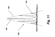
- the sidebands 804 are at optical frequencies, and it is therefore possible to shape them using optical filters. This shaping modifies the microwave signals that are carried by the optical signal, and can therefore be used to perform the apodising function described above without the need for expensive, complex and bulky microwave filters.
- the profile 900 comprises an intensity peak 902 (the carrier signal) and sidebands 904 enclosed within an envelope 906 representing a filter function. It can be seen that the intensity peak 902 is effectively the same as the intensity peak 802 ( Figure 10) of the non-filtered profile. However, the sidebands 904 have progressively decreasing peaks as shown. In order to provide the profile 900, optical filters (not shown) are required.
- fibre Fabry-Perot filters both single and multiple cavity
- Fibre Fabry-Perot filters are similar to bulk etalons, in that they comprise a piece of single-mode fibre with highly reflecting ends, thus forming an electromagnetic cavity.
- Fibre Fabry-Perot filters are also controllable and tuneable.
- the distance between the mirrors can be altered either by slightly heating or cooling the cavity, or by stretching it using piezoelectric drive.
- these filters are available as commercial off-the-shelf components, since they are used regularly in the telecoms industry.
- the fibre Fabry-Perot filters must provide characteristics such as those shown by way of example in Figure 3.
- attempts to fit the Fabry-Perot function of equation (1) above show that the slope of the Fabry-Perot function is too small to provide the required characteristic.
- the maximum rate of intensity with frequency given by the Fabry-Perot function (equation (1) above) is an inverse square response, whereas inverse relationships to the eighth power are required to fit the filter characteristics needed for the outer antenna elements at high frequency (such as that referred to as 36 in Figure 3). Higher power inverse relationships may be required depending on the desired filter characteristic for a given application.
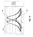
- filter characteristics 1002, 1004 define a new filter characteristic 1006 when they are arranged to overlap.
- This new filter characteristic 1006 exhibits a flatter top, and steeper sides, than either of individual characteristics 1002 or 1004. It is therefore better suited to providing characteristics such as characteristic 36 shown in Figure 3. It can be used, for example, to provide characteristic 906 shown in Figure 11.
- FIG 13 illustrates an alternative overlapping arrangement of filter characteristics 1002, 1004.
- the filters used are centred on the same frequency, rather than separate frequencies as shown in Figure 12. This arrangement produces a narrower filter characteristic 1008.
- FIG 14 illustrates an envelope 1102 that is defined by filter characteristics 1104, 1106.
- Filter characteristics 1104, 1106 correspond to filter characteristics 1002, 1004 ( Figure 13), but they are further apart so that the envelope 1102 also includes a more significant attenuation of the low frequencies, as well as higher attenuation of the higher frequencies.
- each filter characteristic 1104, 1106 its dispersion characteristics 1114, 1116 is also shown in Figure 14. These dispersion characteristics can be summed as illustrated in Figure 15. Elements that have been described previously are referenced the same.
- the sum of the dispersion characteristics 1114, 1116 is referenced as profile 1118. In the region 1120 of profile 1118, the profile is substantially flat. Region 1120, as will readily be appreciated, corresponds to the frequency range in which the envelope 1102 of Figure 14 actively filters the incoming signals.
- filter characteristics may also be obtained using fibre Fabry-Perot filters.
- the above examples provide low-pass filtering characteristics.
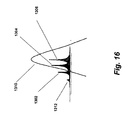
- a high-pass filter can be obtained. This is shown in Figure 16, where the filter characteristic 1310 is offset from the optical carrier frequency 1302, such that the sidebands 1304 and 1306 on the high frequency side of the carrier are transmitted, whereas those on the low frequency side, such as sideband 1312, have much reduced intensity.
- Other components may also be used.
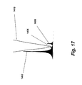
- a notch filter is shown schematically in Figure 17, in which carrier frequency 1402 and sideband 1406 are substantially unaffected by filter characteristic 1410, whereas the intensity of sideband 1404 is dramatically reduced. Such a characteristic is achieved using an optical absorber.
- the apodising function can be achieved with sufficient precision for use in a phased array antenna using combinations of only two Fabry-Perot filters. Whilst it is possible to use more Fabry-Perot filters to achieve more widely varying functions, it is advantageous to keep the numbers used low so as to minimise any potential losses.
- FIG. 18 is a flow diagram to illustrate a method of controlling the optical filters using optical wavelength lockers (OWL's) such as those available from the Santec Corporation.
- OWL optical wavelength lockers
- a portion of the output from each optical filter 1802, 1804 is fed to an OWL 1806, 1808.
- Each filter is provided with an OWL.
- the OWL then feeds back a control signal to the optical filter.
- OWL 1806 feeds back control signal 1810 to filter 1802, and OWL 1808 feeds back control signal 1812 to filter 1804.
- a locker 1820 takes a proportion of the laser signal and feeds back a control signal 1822 to laser 1824.
- the laser 1824 can be modulated with a microwave signal such that its output is the optical signal described above. It is to be appreciated that the method could be applied to all the embodiments using optical filters described above, and is not limited to embodiments in which only two filters are used.
Landscapes
- Variable-Direction Aerials And Aerial Arrays (AREA)
Abstract
Description
- the size of the array aperture
- the number of elements and their placement in the array
- the operating frequency of the array
- the excitation of each element (that is, the amplitude and phase applied to each element)
- the immersed element pattern
- the scattering from the array in the environment in which the antenna array is located
Claims (9)
- A method of controlling beam shape in a phased antenna array comprising the steps of:-(a) receiving signals at an antenna array;(b) apodising the received signals to taper the aperture distribution of the antenna array; and(c) processing the apodised signals.
- A method of controlling beam shape in a phased array antenna comprising the steps of:(a) receiving a signal in a first frequency range at an antenna array;(b) imposing the signal onto a carrier signal, thereby forming a modulated carrier signal;(c) applying an apodising filter to the modulated carrier signal such that the beam shape is substantially constant throughout the first frequency range; and(d) processing the signal.
- A method as claimed in claim 2, wherein the antenna array comprises a number of antenna elements, and the apodising filter comprises a number of fibre Fabry-Perot filters, and wherein each fibre Fabry-Perot filter is associated with one of the number of antenna elements.
- A filter arrangement including at least one apodising filter that provides a frequency-dependent taper on an aperture distribution.
- A filter arrangement for controlling beam shape in a phased array antenna, the phased array antenna comprising a number of antenna elements to receive a signal in a first frequency range, and the apodising filter system comprises a number of channels, wherein one of the number of channels is associated with one of the number of antenna elements and comprises:the number of channels thereby being arranged such that the beam shape is substantially constant across the first frequency range.a frequency converter to impose the signal onto a carrier signal, thereby forming a modulated carrier signal; anda filter element to apply a predetermined filter function to the modulated carrier signal;
- An arrangement as claimed in claim 5 wherein the carrier signal is an optical signal.
- An arrangement as claimed in claim 5 or claim 6 wherein the filter element is a fibre Fabry-Perot filter.
- An arrangement as claimed in claim 5 or claim 6 wherein the filter element is a thin film filter.
- A spatial discriminator including a filter arrangement as claimed in any of claims 4 to 8.
Applications Claiming Priority (4)
| Application Number | Priority Date | Filing Date | Title |
|---|---|---|---|
| GB0410813A GB0410813D0 (en) | 2004-05-14 | 2004-05-14 | Filters |
| GB0410813 | 2004-05-14 | ||
| GB0505311 | 2005-03-16 | ||
| GB0505311A GB0505311D0 (en) | 2005-03-16 | 2005-03-16 | Filters |
Publications (2)
| Publication Number | Publication Date |
|---|---|
| EP1596468A2 true EP1596468A2 (en) | 2005-11-16 |
| EP1596468A3 EP1596468A3 (en) | 2006-01-18 |
Family
ID=34941862
Family Applications (1)
| Application Number | Title | Priority Date | Filing Date |
|---|---|---|---|
| EP05270013A Withdrawn EP1596468A3 (en) | 2004-05-14 | 2005-05-09 | Filters |
Country Status (1)
| Country | Link |
|---|---|
| EP (1) | EP1596468A3 (en) |
Cited By (1)
| Publication number | Priority date | Publication date | Assignee | Title |
|---|---|---|---|---|
| WO2007060478A1 (en) * | 2005-11-23 | 2007-05-31 | Bae Systems Plc | Beam shaping for wide band array antennae |
Family Cites Families (5)
| Publication number | Priority date | Publication date | Assignee | Title |
|---|---|---|---|---|
| US4571594A (en) * | 1983-09-02 | 1986-02-18 | The United States Of America As Represented By The Secretary Of The Air Force | Directional antenna system having sidelobe suppression |
| US6337660B1 (en) * | 1993-09-17 | 2002-01-08 | The United States Of America As Represented By The Secretary Of The Navy | Fiber optic true time-delay array antenna feed system |
| AU3361095A (en) * | 1994-08-05 | 1996-03-04 | Acuson Corporation | Method and apparatus for transmit beamformer system |
| US5751248A (en) * | 1994-10-13 | 1998-05-12 | The Boeing Company | Phased array beam controller using integrated electro-optic circuits |
| FR2838199B1 (en) * | 2002-04-03 | 2004-06-25 | Commissariat Energie Atomique | OPTICAL FILTERING DEVICE |
-
2005
- 2005-05-09 EP EP05270013A patent/EP1596468A3/en not_active Withdrawn
Cited By (3)
| Publication number | Priority date | Publication date | Assignee | Title |
|---|---|---|---|---|
| WO2007060478A1 (en) * | 2005-11-23 | 2007-05-31 | Bae Systems Plc | Beam shaping for wide band array antennae |
| AU2006318826B2 (en) * | 2005-11-23 | 2010-06-10 | Bae Systems Plc | Beam shaping for wide band array antennae |
| US8466848B2 (en) | 2005-11-23 | 2013-06-18 | Bae Systems Plc | Beam shaping for wide band array antennae |
Also Published As
| Publication number | Publication date |
|---|---|
| EP1596468A3 (en) | 2006-01-18 |
Similar Documents
| Publication | Publication Date | Title |
|---|---|---|
| Hunter et al. | Demonstration of a continuously variable true-time delay beamformer using a multichannel chirped fiber grating | |
| US4814773A (en) | Fiber optic feed network for radar | |
| EP3223441B1 (en) | High-capacity communications satellite using passive optical beamforming | |
| Ortega et al. | Variable delay line for phased-array antenna based on a chirped fiber grating | |
| EP0959521B1 (en) | Wideband phased array antennas and method | |
| US6348890B1 (en) | Phased array antenna beamformer | |
| US7558450B2 (en) | Microwave photonic delay line with separate tuning of optical carrier | |
| Ivanov et al. | Application of microwave photonics components for ultrawideband antenna array beamforming | |
| US9748648B2 (en) | Distributed feeding device for antenna beamforming | |
| US9917651B2 (en) | Feed signal generation for a phased array antenna | |
| Roeloffzen et al. | Integrated optical beamformers | |
| Minasian et al. | Optical-fiber grating-based beamforming network for microwave phased arrays | |
| US20020012500A1 (en) | True time delay generating system and method | |
| Subbaraman et al. | Photonic crystal fiber-based true-time-delay beamformer for multiple RF beam transmission and reception of an X-band phased-array antenna | |
| KR102494190B1 (en) | Two-dimensional Directional Optical Phased Array Device | |
| US20090027268A1 (en) | Multi Beam Photonic Beamformer | |
| JP7701669B2 (en) | Transmission directivity control device and transmission directivity control method | |
| JP7744611B2 (en) | Transmission directivity control device and transmission directivity control method | |
| DK1952481T3 (en) | FORMATION OF RADIATIONS FOR BROADBAND ANTENNA GROUPS | |
| Goutzoulis et al. | Development and field demonstration of an eight-element receive wavelength-multiplexed true-time-delay steering system | |
| WO2025017809A1 (en) | Transmission directivity control device and transmission directivity control method | |
| EP4465080A2 (en) | Optical beam forming device with crossbar as beamformer and its method of use | |
| WO2026074701A1 (en) | Transmission directivity control apparatus | |
| US10073221B2 (en) | Beamforming for an optical switch | |
| JP7751241B2 (en) | Transmission directivity control device and control method |
Legal Events
| Date | Code | Title | Description |
|---|---|---|---|
| PUAI | Public reference made under article 153(3) epc to a published international application that has entered the european phase |
Free format text: ORIGINAL CODE: 0009012 |
|
| AK | Designated contracting states |
Kind code of ref document: A2 Designated state(s): AT BE BG CH CY CZ DE DK EE ES FI FR GB GR HU IE IS IT LI LT LU MC NL PL PT RO SE SI SK TR |
|
| AX | Request for extension of the european patent |
Extension state: AL BA HR LV MK YU |
|
| PUAL | Search report despatched |
Free format text: ORIGINAL CODE: 0009013 |
|
| AK | Designated contracting states |
Kind code of ref document: A3 Designated state(s): AT BE BG CH CY CZ DE DK EE ES FI FR GB GR HU IE IS IT LI LT LU MC NL PL PT RO SE SI SK TR |
|
| AX | Request for extension of the european patent |
Extension state: AL BA HR LV MK YU |
|
| RAP1 | Party data changed (applicant data changed or rights of an application transferred) |
Owner name: SELEX SENSORS AND AIRBORNE SYSTEMS LIMITED |
|
| AKX | Designation fees paid | ||
| REG | Reference to a national code |
Ref country code: DE Ref legal event code: 8566 |
|
| STAA | Information on the status of an ep patent application or granted ep patent |
Free format text: STATUS: THE APPLICATION IS DEEMED TO BE WITHDRAWN |
|
| 18D | Application deemed to be withdrawn |
Effective date: 20060719 |