EP1596421A2 - Lithographic apparatus and device manufacturing method - Google Patents
Lithographic apparatus and device manufacturing method Download PDFInfo
- Publication number
- EP1596421A2 EP1596421A2 EP04076427A EP04076427A EP1596421A2 EP 1596421 A2 EP1596421 A2 EP 1596421A2 EP 04076427 A EP04076427 A EP 04076427A EP 04076427 A EP04076427 A EP 04076427A EP 1596421 A2 EP1596421 A2 EP 1596421A2
- Authority
- EP
- European Patent Office
- Prior art keywords
- load lock
- gas
- pressure
- door
- radiation
- Prior art date
- Legal status (The legal status is an assumption and is not a legal conclusion. Google has not performed a legal analysis and makes no representation as to the accuracy of the status listed.)
- Withdrawn
Links
Images

Classifications
-
- H—ELECTRICITY
- H10—SEMICONDUCTOR DEVICES; ELECTRIC SOLID-STATE DEVICES NOT OTHERWISE PROVIDED FOR
- H10P—GENERIC PROCESSES OR APPARATUS FOR THE MANUFACTURE OR TREATMENT OF DEVICES COVERED BY CLASS H10
- H10P72/00—Handling or holding of wafers, substrates or devices during manufacture or treatment thereof
- H10P72/04—Apparatus for manufacture or treatment
- H10P72/0451—Apparatus for manufacturing or treating in a plurality of work-stations
- H10P72/0468—Apparatus for manufacturing or treating in a plurality of work-stations comprising a chamber adapted to a particular process
- H10P72/0474—Apparatus for manufacturing or treating in a plurality of work-stations comprising a chamber adapted to a particular process comprising at least one lithography chamber
-
- G—PHYSICS
- G03—PHOTOGRAPHY; CINEMATOGRAPHY; ANALOGOUS TECHNIQUES USING WAVES OTHER THAN OPTICAL WAVES; ELECTROGRAPHY; HOLOGRAPHY
- G03F—PHOTOMECHANICAL PRODUCTION OF TEXTURED OR PATTERNED SURFACES, e.g. FOR PRINTING, FOR PROCESSING OF SEMICONDUCTOR DEVICES; MATERIALS THEREFOR; ORIGINALS THEREFOR; APPARATUS SPECIALLY ADAPTED THEREFOR
- G03F7/00—Photomechanical, e.g. photolithographic, production of textured or patterned surfaces, e.g. printing surfaces; Materials therefor, e.g. comprising photoresists; Apparatus specially adapted therefor
- G03F7/70—Microphotolithographic exposure; Apparatus therefor
- G03F7/708—Construction of apparatus, e.g. environment aspects, hygiene aspects or materials
- G03F7/70808—Construction details, e.g. housing, load-lock, seals or windows for passing light in or out of apparatus
-
- G—PHYSICS
- G03—PHOTOGRAPHY; CINEMATOGRAPHY; ANALOGOUS TECHNIQUES USING WAVES OTHER THAN OPTICAL WAVES; ELECTROGRAPHY; HOLOGRAPHY
- G03F—PHOTOMECHANICAL PRODUCTION OF TEXTURED OR PATTERNED SURFACES, e.g. FOR PRINTING, FOR PROCESSING OF SEMICONDUCTOR DEVICES; MATERIALS THEREFOR; ORIGINALS THEREFOR; APPARATUS SPECIALLY ADAPTED THEREFOR
- G03F7/00—Photomechanical, e.g. photolithographic, production of textured or patterned surfaces, e.g. printing surfaces; Materials therefor, e.g. comprising photoresists; Apparatus specially adapted therefor
- G03F7/70—Microphotolithographic exposure; Apparatus therefor
- G03F7/708—Construction of apparatus, e.g. environment aspects, hygiene aspects or materials
- G03F7/70908—Hygiene, e.g. preventing apparatus pollution, mitigating effect of pollution or removing pollutants from apparatus
- G03F7/70933—Purge, e.g. exchanging fluid or gas to remove pollutants
-
- H—ELECTRICITY
- H10—SEMICONDUCTOR DEVICES; ELECTRIC SOLID-STATE DEVICES NOT OTHERWISE PROVIDED FOR
- H10P—GENERIC PROCESSES OR APPARATUS FOR THE MANUFACTURE OR TREATMENT OF DEVICES COVERED BY CLASS H10
- H10P72/00—Handling or holding of wafers, substrates or devices during manufacture or treatment thereof
- H10P72/04—Apparatus for manufacture or treatment
- H10P72/0451—Apparatus for manufacturing or treating in a plurality of work-stations
- H10P72/0466—Apparatus for manufacturing or treating in a plurality of work-stations characterised by the construction of the load-lock chamber
Definitions
- the present invention relates to a lithographic projection apparatus comprising:
- the invention further relates to a device manufacturing method.
- patterning means as here employed should be broadly interpreted as referring to means that can be used to endow an incoming radiation beam with a patterned cross-section, corresponding to a pattern that is to be created in a target portion of the substrate; the term “light valve” can also be used in this context.
- the said pattern will correspond to a particular functional layer in a device being created in the target portion, such as an integrated circuit or other device (see below). Examples of such patterning means include:
- Lithographic projection apparatus can be used, for example, in the manufacture of integrated circuits (ICs).
- the patterning means may generate a circuit pattern corresponding to an individual layer of the IC, and this pattern can be imaged onto a target portion (e.g. comprising one or more dies) on a substrate (silicon wafer) that has been coated with a layer of radiation-sensitive material (resist).
- a target portion e.g. comprising one or more dies
- a substrate silicon wafer
- a layer of radiation-sensitive material resist
- a single wafer will contain a whole network of adjacent target portions that are successively irradiated via the projection system, one at a time.
- employing patterning by a mask on a mask table a distinction can be made between two different types of machine.
- each target portion is irradiated by exposing the entire mask pattern onto the target portion in one go; such an apparatus is commonly referred to as a wafer stepper or step-and-repeat apparatus.
- a wafer stepper or step-and-repeat apparatus In an alternative apparatus ⁇ commonly referred to as a step-and-scan apparatus ⁇ each target portion is irradiated by progressively scanning the mask pattern under the projection beam in a given reference direction (the "scanning" direction) while synchronously scanning the substrate table parallel or anti-parallel to this direction; since, in general, the projection system will have a magnification factor M (generally ⁇ 1), the speed V at which the substrate table is scanned will be a factor M times that at which the mask table is scanned. More information with regard to lithographic devices as here described can be gleaned, for example, from US 6,046,792, incorporated herein by reference.
- a pattern (e.g. in a mask) is imaged onto a substrate that is at least partially covered by a layer of radiation-sensitive material (resist).
- the substrate Prior to this imaging step, the substrate may undergo various procedures, such as priming, resist coating and a soft bake. After exposure, the substrate may be subjected to other procedures, such as a post-exposure bake (PEB), development, a hard bake and measurement/inspection of the imaged features.
- PEB post-exposure bake
- This array of procedures is used as a basis to pattern an individual layer of a device, e.g. an IC.
- Such a patterned layer may then undergo various processes such as etching, ion-implantation (doping), metallization, oxidation, chemo-mechanical polishing, etc., all intended to finish off an individual layer. If several layers are required, then the whole procedure, or a variant thereof, will have to be repeated for each new layer. Eventually, an array of devices will be present on the substrate (wafer). These devices are then separated from one another by a technique such as dicing or sawing, whence the individual devices can be mounted on a carrier, connected to pins, etc.
- the projection system may hereinafter be referred to as the "lens"; however, this term should be broadly interpreted as encompassing various types of projection systems, including refractive optics, reflective optics, and catadioptric systems, for example.
- the radiation system may also include components operating according to any of these design types for directing, shaping or controlling the projection beam of radiation, and such components may also be referred to below, collectively or singularly, as a "lens".
- the lithographic apparatus may be of a type having two or more substrate tables (and/or two or more mask tables).
- UV radiation e.g. with a wavelength of 365, 248, 193, 157 or 126 nm
- EUV extreme ultra-violet
- particle beams such as ion beams or electron beams.
- a lithographic projection apparatus usually comprises two or more different chambers, such as a handling chamber and a patterning chamber. Particularly in applications using EUV radiation, vacuum conditions are maintained in some or all of these chambers.
- a load lock is a chamber, that comprises at least two doors, where a first door typically faces vacuum conditions, having a pressure P vac , and a second door typically faces atmospheric conditions, having a pressure P atm .
- a first door typically faces vacuum conditions, having a pressure P vac
- a second door typically faces atmospheric conditions, having a pressure P atm .
- a substrate from the atmospheric environment to the vacuum environment via the load lock usually comprises the following steps:
- the movement of a substrate in the opposite direction i.e. from the vacuum conditions to the atmospheric conditions, usually comprises the following steps:
- the use of such a load lock can have a few disadvantages.
- pumping down the load lock is preferably done as quickly as possible, in order to achieve a high throughput.
- the temperature of the gas in the load lock may drop (adiabatic process).
- the gasses in the load lock may contain water, which condenses as a result of the temperature drop.
- the condensation nuclei are particles that can drop on the substrate that is transported to the vacuum conditions. These particles contaminate the substrate and subsequently, for example, the substrate handling chamber and the exposure chamber.
- the load lock comprises a gas, that contains water
- the water molecules tend to stick to the walls of the load lock due to adhesive forces. This has a negative impact on the pumping down time of the load lock.
- the content of the load lock gasses
- the vacuum space such as the wafer handling chamber and the exposure chamber. If this space contains oxygen and/or hydrocarbons and/or H 2 O, this can result, in combination with EUV radiation, in degradation of the process related components, such as contaminated optics. If the volume in the load lock comprises particles, these particles can contaminate the substrates being transported by the load lock as well process related components.
- substrates being transported can absorb or chemically bond with oxygen, hydrocarbons and/or H 2 O.
- oxygen hydrocarbons and/or H 2 O.
- the substrate might gas out, also causing degradation of the process related components.
- This and other objects are achieved according to the invention in a lithographic projection apparatus, characterized in that the gas inlet is connected to a gas supply that supplies, at least during part of the transfer of the object a gas to the gas inlet, the gas being essentially free from at least one of particles, oxygen, hydrocarbon and H 2 O.
- Venting the load lock with such a gas reduces the migration of hazardous particles into the load lock, and also reduces molecular contamination, for instance by oxygen, hydrocarbon and H 2 O, in the load lock.
- the absence of these particles and/or molecules has a positive effect on the pump down time of the load lock.
- the further migration of these particles and/or molecules to the inside of the lithographic projection apparatus can be limited.
- the lithography patterning chamber has a first pressure and the second environment has a second pressure, the first pressure being lower than the second pressure.
- Load locks are advantageously used for transferring objects between a first pressure and a second pressure.
- the load lock is vented to a third pressure that is higher than the second pressure.
- a third pressure that is higher than the second pressure.
- the load lock is vented when the second door is open. This will even further reduce the migration of hazardous particles and contaminating molecules to the load lock. Such continued venting creates a flow out of the load lock to the environment, reducing the migration of hazardous gas particles and contaminating molecules from the environment into the load lock.
- the object is selected from a group of objects used in a lithographic projection apparatus, including a mask or a wafer.
- a lithographic projection apparatus including a mask or a wafer.
- the gas is one of N 2 gas, Ar gas and synthetic air. These gasses are free from contaminating particles and are also free from contaminating molecules, such as hydrocarbon and H 2 O. These gasses are also readily available.
- a gas outlet is connected to the gas supply. This makes it possible to re-use the gas that is essentially free from oxygen and/or hydrocarbon and/or H 2 O.
- the gas outlet is connected to the gas supply via a filter system.
- the present invention relates to a device manufacturing method comprising:
- Figure 1 schematically depicts a lithographic projection apparatus 1 according to a particular embodiment of the invention.
- the apparatus comprises:
- the apparatus is of a reflective type (i.e. has a reflective mask). However, in general, it may also be of a transmissive type, for example with a transmissive mask. Alternatively, the apparatus may employ another kind of patterning means, such as a programmable mirror array of a type as referred to above.
- the source LA (e.g. EUV source) produces a beam of radiation.
- This beam is fed into an illumination system (illuminator) IL, either directly or after having traversed conditioning means, such as a beam expander Ex, for example.
- the illuminator IL may comprise adjusting means AM for setting the outer and/or inner radial extent (commonly referred to as ⁇ -outer and ⁇ -inner, respectively) of the intensity distribution in the beam.
- ⁇ -outer and ⁇ -inner commonly referred to as ⁇ -outer and ⁇ -inner, respectively
- it will generally comprise various other components, such as an integrator IN and a condenser CO.
- the beam PB impinging on the mask MA has a desired uniformity and intensity distribution in its cross-section.
- the source LA may be within the housing of the lithographic projection apparatus (as is often the case when the source LA is a mercury lamp, for example), but that it may also be remote from the lithographic projection apparatus, the radiation beam which it produces being led into the apparatus (e.g. with the aid of suitable directing mirrors); this latter scenario is often the case when the source LA is an excimer laser.
- the current invention and claims encompass both of these scenarios.
- the beam PB subsequently intercepts the mask MA, which is held on a mask table MT. Having traversed the mask MA, the beam PB passes through the lens PL, which focuses the beam PB onto a target portion C of the substrate W. With the aid of the second positioning means PW (and interferometric measuring means IF), the substrate table WT can be moved accurately, e.g. so as to position different target portions C in the path of the beam PB. Similarly, the first positioning means PM can be used to accurately position the mask MA with respect to the path of the beam PB, e.g. after mechanical retrieval of the mask MA from a mask library, or during a scan.
- the mask table MT may just be connected to a short stroke actuator, or may be fixed.
- Mask MA and substrate W may be aligned using mask alignment marks M1, M2 and substrate alignment marks P1, P2.
- the depicted apparatus can be used in two different modes:
- Fig. 2 schematically depicts a load lock LL according to an embodiment of the present invention.
- the load lock LL comprises two doors 11, 12.
- the first door 11 faces the inside of the lithographic projection apparatus 1, comprising the handling chamber HC and the lithography patterning chamber PC, in which vacuum conditions, having a pressure P vac , are maintained.
- the second door 12 faces atmospheric conditions, having a pressure that is, for instance, equal to atmospheric pressure P atm .
- the invention can also advantageously be applied for other pressure values.
- the load lock LL comprises a wall that forms an inner space.
- the load lock LL is further provided with supporting means (not shown) for supporting one or more objects, such as substrates, as will be known to a person skilled in the art.
- the load lock LL is also provided with a gas inlet 13 and a gas outlet 15.
- the gas outlet 15 can be provided with a pump 16 to pump down the load lock LL to vacuum conditions of, for instance, 10 -3 - 10 -5 Pa, a pressure substantially equal to or lower than P vac .
- the movement of, for instance, a substrate W from the atmospheric environment to the vacuum via the load lock LL usually comprises the following steps:
- the gas inlet 13 can be used to vent the load lock in order to raise the pressure in the load lock from P vac to P atm .
- Movement of a substrate W from the vacuum to the atmospheric environment via the load lock LL usually comprises the following steps:
- hazardous particles and contaminating molecules such as oxygen, hydrocarbons and/or H 2 O
- a specially chosen gas that doesn't comprise these particles or molecules.
- Gasses such as N 2 gas, Ar gas or synthetic air, but of course also other suitable gasses, can be used, as will be understood by a person skilled in the art.
- FIG. 2 shows a gas supply 17 comprising N 2 gas.
- Gas supply 17 may be a high pressure tank.
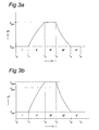
- Figure 3a shows a graph of the pressure P in the load lock LL with respect to time t, during a pumping and venting cycle of the load lock LL, in which, e.g. wafers W can be exchanged between the first and second environment.
- the graph is divided into five segments I, II, III, IV and V.
- phase I from to to t 1 , the pressure in the load lock LL is substantially equal to or less than P vac .
- the first door 11 facing the vacuum conditions can be opened to transfer substrate W, or the like, to or from the load lock LL.
- the first door 11 is closed.
- phase II from t 1 to t 2 , the pressure in the load lock LL is brought back to substantially P atm , by venting the load lock LL via the gas inlet 13 with a suitable gas.
- the load lock LL is vented with N 2 gas. Gas inlet 13 is connected to the gas supply 17.
- the load lock is at substantially atmospheric pressure and filled with N 2 gas and the second door 12 facing the atmospheric conditions can be opened.
- the substrate W or the like can be transferred to or from the load lock LL.
- the load lock LL Since the load lock LL is filled with N 2 gas almost no hazardous particles or contaminating molecules will enter the load lock during phase III, when the second door 12 is opened. However, some particles and/or molecules may migrate into the load lock LL.
- an overpressure P atm+ is established in the load lock LL during phase III, as can be seen in Fig. 3b.
- This overpressure P atm+ can be realized by continuing the inflow of N 2 gas through gas inlet 13 during phase III, even when the second door 12 is open.
- the overpressure will cause a gas flow from the load lock LL to the atmospheric environment, minimizing the migration of particles and/or molecules from the atmospheric environment to the load lock LL.
- the second door 12 is closed and during phase IV, the load lock LL is pumped down to substantially equal to or less than P vac via gas outlet 15 by pump 16.
- the gas that is pumped down from the load lock LL is substantially the gas that was supplied to the load lock LL, namely the N 2 gas.
- the gas outlet 15 can be connected to the gas supply 17, for instance via a filter system (not shown), to re-use the N 2 gas.
Landscapes
- Health & Medical Sciences (AREA)
- Epidemiology (AREA)
- Public Health (AREA)
- Engineering & Computer Science (AREA)
- Environmental & Geological Engineering (AREA)
- Physics & Mathematics (AREA)
- General Physics & Mathematics (AREA)
- Life Sciences & Earth Sciences (AREA)
- Atmospheric Sciences (AREA)
- Container, Conveyance, Adherence, Positioning, Of Wafer (AREA)
- Electron Beam Exposure (AREA)
- Exposure And Positioning Against Photoresist Photosensitive Materials (AREA)
Abstract
Description
- a radiation system for providing a projection beam of radiation;
- a lithography patterning chamber comprising:
- a support structure for supporting patterning means, the patterning means serving to pattern the projection beam according to a desired pattern;
- a substrate table for holding a substrate; and
- a projection system for projecting the patterned beam onto a target portion of the substrate; and
- a load lock for transferring an object from the lithography patterning chamber to a second environment or vice versa, the load lock defining a chamber and comprising a first door facing the lithography patterning chamber, and a second door facing the second environment, and the load lock further comprising a gas inlet for venting the load lock.
- A mask. The concept of a mask is well known in lithography, and it includes mask types such as binary, alternating phase-shift, attenuated phase-shift, as well as various hybrid mask types. Placement of such a mask in the radiation beam causes selective transmission (in the case of a transmissive mask) or reflection (in the case of a reflective mask) of the radiation impinging on the mask, according to the pattern on the mask. In the case of a mask, the support structure will generally be a mask table, which ensures that the mask can be held at a desired position in the incoming radiation beam, and that it can be moved relative to the beam if so desired;
- A programmable mirror array. One example of such a device is a matrix-addressable surface having a viscoelastic control layer and a reflective surface. The basic principle behind such an apparatus is that (for example) addressed areas of the reflective surface reflect incident light as diffracted light, whereas unaddressed areas reflect incident light as undiffracted light. Using an appropriate filter, the said undiffracted light can be filtered out of the reflected beam, leaving only the diffracted light behind; in this manner, the beam becomes patterned according to the addressing pattern of the matrix-addressable surface. An alternative embodiment of a programmable mirror array employs a matrix arrangement of tiny mirrors, each of which can be individually tilted about an axis by applying a suitable localized electric field, or by employing piezoelectric actuation means. Once again, the mirrors are matrix-addressable, such that addressed mirrors will reflect an incoming radiation beam in a different direction to unaddressed mirrors; in this manner, the reflected beam is patterned according to the addressing pattern of the matrix-addressable mirrors. The required matrix addressing can be performed using suitable electronic means. In both of the situations described hereabove, the patterning means can comprise one or more programmable mirror arrays. More information on mirror arrays as here referred to can be gleaned, for example, from United States Patents US 5,296,891 and US 5,523,193, and PCT patent applications WO 98/38597 and WO 98/33096, which are incorporated herein by reference. In the case of a programmable mirror array, the said support structure may be embodied as a frame or table, for example, which may be fixed or movable as required; and
- A programmable LCD array. An example of such a construction is given in United States Patent US 5,229,872, which is incorporated herein by reference. As above, the support structure in this case may be embodied as a frame or table, for example, which may be fixed or movable as required.
- opening the second door facing the atmospheric conditions Patm,
- delivering the substrate from atmospheric conditions Patm in the load lock,
- closing the second door,
- pumping down the load lock to vacuum conditions Pvac,
- opening the first door facing the vacuum conditions Pvac, and
- delivering the substrate from the load lock to the vacuum conditions Pvac.
- opening the first door facing the vacuum conditions Pvac,
- delivering the substrate from the vacuum conditions Pvac into the load lock,
- closing the first door,
- venting the load lock to atmospheric conditions Patm,
- opening the second door facing the atmospheric conditions Patm, and
- delivering the substrate from the load lock to the atmospheric conditions Patm.
- providing a substrate that is at least partially covered by a layer of radiation-sensitive material in a lithography patterning chamber;
- providing a projection beam of radiation using a radiation system;
- using patterning means to endow the projection beam with a pattern in its cross-section; and
- projecting the patterned beam of radiation onto a target portion of the layer of radiation-sensitive material,
- transferring the substrate from and to said lithography patterning chamber via a load lock, the load lock defining a chamber and comprising a first door facing the lithography patterning chamber and a second door facing a second environment,
venting the load lock with a gas that is essentially free from at least one of particles, oxygen, hydrocarbon and H2O at least during part of the transfer.
- Figure 1 depicts a lithographic projection apparatus according to an embodiment of the invention;
- Figure 2 schematically depicts a load lock according to an embodiment of the present invention; and
- Figure 3a and 3b depict a graph of the pressure in the load lock with respect to the time, according to an embodiment of the present invention.
- a radiation system Ex, IL, for supplying a projection beam PB of radiation (e.g. EUV radiation). In this particular case, the radiation system also comprises a radiation source LA;
- a first object table (mask table) MT provided with a mask holder for holding a mask MA (e.g. a reticle), and connected to first positioning means PM for accurately positioning the mask with respect to item PL;
- a second object table (substrate table) WT provided with a substrate holder for holding a substrate W (e.g. a resist-coated silicon wafer), and connected to second positioning means PW for accurately positioning the substrate with respect to item PL; and
- a projection system ("lens") PL (e.g. mirrors for EUV radiation) for imaging an irradiated portion of the mask MA onto a target portion C (e.g. comprising one or more dies) of the substrate W.
- opening the
second door 12 facing the atmospheric conditions Patm, - transferring the substrate W from atmospheric conditions Patm into the load lock LL,
- closing the
second door 12, - pumping down the load lock LL to a pressure substantially equal to or less
than vacuum conditions Pvac through
gas outlet 15 usingpump 16, - opening the
first door 11 facing the vacuum conditions Pvac, and - transferring the substrate W to the vacuum conditions Pvac from the load lock LL.
- pumping down the load lock LL to a pressure substantially equal to or less than the vacuum conditions Pvac,
- opening the
first door 11 facing the vacuum conditions Pvac, - transferring the substrate W from the vacuum conditions Pvac into the load lock LL,
- closing the
first door 11, - venting the load lock LL to a pressure substantially equal to or more than
atmospheric conditions Patm via the
gas inlet 13, - opening the
second door 12 facing the atmospheric conditions Patm, and - delivering the substrate W to the atmospheric conditions Patm.
Claims (15)
- A lithographic projection apparatus comprising:characterized in thata radiation system for providing a projection beam (PB) of radiation;a lithography patterning chamber (PC) comprisinga support structure (MT) for supporting patterning means (MA), the patterning means (MA) serving to pattern the projection beam (PB) according to a desired pattern;a substrate table (WT) for holding a substrate (W); anda projection system (PL) for projecting the patterned beam onto a target portion (C) of the substrate (W); anda load lock (LL) for transferring an object (MA, W) from the lithography patterning chamber (PC) to a second environment or vice versa, the load lock defining a chamber and comprising a first door (11) facing the lithography patterning chamber (PC), and a second door (12) facing the second environment, and the load lock (LL) further comprising a gas inlet (13) for venting the load lock (LL),
the gas inlet (13) is connected to a gas supply (17) that supplies, at least during part of the transfer of the object a gas to the gas inlet (13), the gas being essentially free from at least one of particles, oxygen, hydrocarbon and H2O. - A lithographic projection apparatus according to claim 1, wherein the lithography patterning chamber (PC) has a first pressure (Pvac) and the second environment has a second pressure (Patm), the first pressure (Pvac) being lower than the second pressure (Patm).
- A lithographic projection apparatus according to claim 1 or 2, wherein the load lock (LL) further comprises a gas outlet (15) connected to a pump (16) that pumps gas out of the load lock (LL) via the gas outlet (15).
- A lithographic projection apparatus according to claim 3, wherein the gas outlet (15) is connected to the gas supply (17).
- A lithographic projection apparatus according to any of the claims 1 - 4, wherein the load lock (LL) is vented to a third pressure (Patm+) that is higher than the second pressure (Patm).
- A lithographic projection apparatus according to any of the preceding claims, wherein the load lock (LL) is vented when the second door (12) is open.
- A lithographic projection apparatus according to any of the preceding claims, wherein the gas is one of N2 gas, Ar gas and synthetic air.
- A device manufacturing method comprising:characterized byproviding a substrate (W) that is at least partially covered by a layer of radiation-sensitive material in a lithography patterning chamber (PC);providing a projection beam (PB) of radiation using a radiation system;using patterning means (MA) to endow the projection beam (PB) with a pattern in its cross-section;projecting the patterned beam of radiation onto a target portion (C) of the layer of radiation-sensitive material; andtransferring the substrate (W) from and to said lithography patterning chamber (PC) via a load lock (LL), the load lock (LL) defining a chamber and comprising a first door (11) facing the lithography patterning chamber (PC) and a second door (12) facing a second environment,
venting the load lock (LL) with a gas that is essentially free from at least one of particles, oxygen, hydrocarbon and H2O at least during part of the transfer. - Method according to claim 8, wherein the lithography patterning chamber (PC) has a first pressure (Pvac) and the second environment has a second pressure (Patm), the first pressure (Pvac) being lower than the second pressure (Patm).
- Method according to claim 9, wherein a transfer from the lithography patterning chamber (PC) to the second environment comprises:pumping down the load lock (LL) to substantially equal to or less than the first pressure (Pvac),opening the first door (11),transferring the object (W) from the lithography patterning chamber (PC) into the load lock (LL),closing the first door (11),venting the load lock (LL) with a gas that is essentially free from at least one of particles, oxygen, hydrocarbon and H2O to substantially equal or to more than the second pressure (Patm),opening the second door (12)transferring the object (W) to the second environment.
- Method according to any of claims 8-10, wherein the load lock (LL) is vented to a third pressure (Patm+) that is higher than the second pressure (Patm).
- Method according to any of claims 8-11, wherein the load lock (LL) is vented when the second door (12) is open.
- Method according to any of claims 8 -12, wherein the object is at least one of a mask (MA) or a wafer (W).
- Method according to any of claims 8-13, where the gas is one of N2 gas, Ar gas and synthetic air.
- A device manufacturing method comprising:characterized byproviding a substrate (W) that is at least partially covered by a layer of radiation-sensitive material in a lithography patterning chamber (PC);providing a projection beam (PB) of radiation using a radiation system;using patterning means (MA) to endow the projection beam (PB) with a pattern in its cross-section;projecting the patterned beam of radiation onto a target portion (C) of the layer of radiation-sensitive material; andtransferring an object from and to said lithography patterning chamber (PC) via a load lock (LL), the load lock (LL) defining a chamber and comprising a first door (11) facing the lithography patterning chamber (PC) and a second door (12) facing a second environment, the object being one of said substrate (W) and said patterning means (MA),
venting the load lock (LL) with a gas that is essentially free from at least one of particles, oxygen, hydrocarbon and H2O at least during part of the transfer.
Priority Applications (1)
| Application Number | Priority Date | Filing Date | Title |
|---|---|---|---|
| EP04076427A EP1596421A3 (en) | 2003-05-19 | 2004-05-13 | Lithographic apparatus and device manufacturing method |
Applications Claiming Priority (3)
| Application Number | Priority Date | Filing Date | Title |
|---|---|---|---|
| EP03076498 | 2003-05-19 | ||
| EP03076498 | 2004-05-09 | ||
| EP04076427A EP1596421A3 (en) | 2003-05-19 | 2004-05-13 | Lithographic apparatus and device manufacturing method |
Publications (2)
| Publication Number | Publication Date |
|---|---|
| EP1596421A2 true EP1596421A2 (en) | 2005-11-16 |
| EP1596421A3 EP1596421A3 (en) | 2011-04-06 |
Family
ID=35445972
Family Applications (1)
| Application Number | Title | Priority Date | Filing Date |
|---|---|---|---|
| EP04076427A Withdrawn EP1596421A3 (en) | 2003-05-19 | 2004-05-13 | Lithographic apparatus and device manufacturing method |
Country Status (1)
| Country | Link |
|---|---|
| EP (1) | EP1596421A3 (en) |
Cited By (1)
| Publication number | Priority date | Publication date | Assignee | Title |
|---|---|---|---|---|
| WO2007127068A1 (en) * | 2006-04-24 | 2007-11-08 | Axcelis Technologies, Inc. | Load lock control |
Family Cites Families (7)
| Publication number | Priority date | Publication date | Assignee | Title |
|---|---|---|---|---|
| JP2770960B2 (en) * | 1988-10-06 | 1998-07-02 | キヤノン株式会社 | SOR-X-ray exposure equipment |
| US5314541A (en) * | 1991-05-28 | 1994-05-24 | Tokyo Electron Limited | Reduced pressure processing system and reduced pressure processing method |
| TW332311B (en) * | 1996-03-08 | 1998-05-21 | Nat Denki Kk | The substrate treatment apparatus |
| US5855681A (en) * | 1996-11-18 | 1999-01-05 | Applied Materials, Inc. | Ultra high throughput wafer vacuum processing system |
| US6375746B1 (en) * | 1998-07-10 | 2002-04-23 | Novellus Systems, Inc. | Wafer processing architecture including load locks |
| US7076920B2 (en) * | 2000-03-22 | 2006-07-18 | Mks Instruments, Inc. | Method of using a combination differential and absolute pressure transducer for controlling a load lock |
| JP4560182B2 (en) * | 2000-07-06 | 2010-10-13 | キヤノン株式会社 | Decompression processing apparatus, semiconductor manufacturing apparatus, and device manufacturing method |
-
2004
- 2004-05-13 EP EP04076427A patent/EP1596421A3/en not_active Withdrawn
Cited By (2)
| Publication number | Priority date | Publication date | Assignee | Title |
|---|---|---|---|---|
| WO2007127068A1 (en) * | 2006-04-24 | 2007-11-08 | Axcelis Technologies, Inc. | Load lock control |
| US7381969B2 (en) | 2006-04-24 | 2008-06-03 | Axcelis Technologies, Inc. | Load lock control |
Also Published As
| Publication number | Publication date |
|---|---|
| EP1596421A3 (en) | 2011-04-06 |
Similar Documents
| Publication | Publication Date | Title |
|---|---|---|
| US20040165159A1 (en) | Lithographic apparatus and device manufacturing method | |
| US7130049B2 (en) | Method of measurement, method for providing alignment marks, and device manufacturing method | |
| US7106412B2 (en) | Lithographic apparatus comprising a gas flushing system | |
| EP1429189B1 (en) | Lithographic apparatus and device manufacturing method | |
| US6583858B2 (en) | Substrate holder for lithographic apparatus | |
| US6747730B2 (en) | Lithographic apparatus, device manufacturing method, and method of manufacturing an optical element | |
| EP1319982A1 (en) | Lithographic apparatus , device manufacturing method, and computer program | |
| US7123344B2 (en) | Lithographic apparatus and device manufacturing method | |
| US6707530B2 (en) | Lithographic apparatus, device manufacturing method, and device manufactured thereby | |
| US20050002003A1 (en) | Lithographic apparatus and device manufacturing method | |
| EP1582927A1 (en) | Lithographic apparatus and device manufacturing method | |
| US6714279B2 (en) | Lithographic projection apparatus, device manufacturing method and device manufactured thereby | |
| EP1349010A1 (en) | Lithographic apparatus and device manufacturing method | |
| US7088421B2 (en) | Lithographic apparatus, device manufacturing method, and device manufactured thereby | |
| US20040105083A1 (en) | Lithographic apparatus and device manufacturing method | |
| US7244534B2 (en) | Device manufacturing method | |
| EP1256847B1 (en) | Lithographic apparatus with purge gas system | |
| EP1186958B1 (en) | Lithographic projection apparatus | |
| JP4331099B2 (en) | Lithographic apparatus and device manufacturing method | |
| EP1318431A1 (en) | Lithographic apparatus, device manufacturing method, and method of manufacturing an optical element | |
| EP1396759A2 (en) | Lithographic apparatus, device manufacturing method, and device manufactured thereby | |
| US7256863B2 (en) | Sealing assembly, a lithographic projection apparatus, and a device manufacturing method | |
| EP1333329B1 (en) | Lithographic apparatus and device manufacturing method | |
| EP1500987A1 (en) | Lithographic apparatus, device manufacturing method, and device manufactured thereby | |
| EP1248148A1 (en) | Lithographic patterning means with protective layer |
Legal Events
| Date | Code | Title | Description |
|---|---|---|---|
| PUAI | Public reference made under article 153(3) epc to a published international application that has entered the european phase |
Free format text: ORIGINAL CODE: 0009012 |
|
| AK | Designated contracting states |
Kind code of ref document: A2 Designated state(s): AT BE BG CH CY CZ DE DK EE ES FI FR GB GR HU IE IT LI LU MC NL PL PT RO SE SI SK TR |
|
| AX | Request for extension of the european patent |
Extension state: AL HR LT LV MK |
|
| PUAL | Search report despatched |
Free format text: ORIGINAL CODE: 0009013 |
|
| AK | Designated contracting states |
Kind code of ref document: A3 Designated state(s): AT BE BG CH CY CZ DE DK EE ES FI FR GB GR HU IE IT LI LU MC NL PL PT RO SE SI SK TR |
|
| AX | Request for extension of the european patent |
Extension state: AL HR LT LV MK |
|
| 17P | Request for examination filed |
Effective date: 20110919 |
|
| AKX | Designation fees paid |
Designated state(s): AT BE BG CH CY CZ DE DK EE ES FI FR GB GR HU IE IT LI LU MC NL PL PT RO SE SI SK TR |
|
| 17Q | First examination report despatched |
Effective date: 20130402 |
|
| STAA | Information on the status of an ep patent application or granted ep patent |
Free format text: STATUS: THE APPLICATION IS DEEMED TO BE WITHDRAWN |
|
| 18D | Application deemed to be withdrawn |
Effective date: 20130813 |