BACKGROUND
An Electronic Article Surveillance (EAS) system is designed to prevent
unauthorized removal of an item from a controlled area. A typical EAS system
may comprise a monitoring system and one or more security tags. The
monitoring system may create an interrogation zone at an access point for the
controlled area. A security tag may be fastened to an item, such as an article of
clothing. If the tagged item enters the interrogation zone, an alarm may be
triggered indicating unauthorized removal of the tagged item from the controlled
area.
Desirable properties for an EAS system may include having larger
interrogation zones and smaller, more flexible, security tags. These properties,
however, are typically inversely proportional. For example, EAS systems using
microwave signals typically have wider coverage areas but need larger security
tags. Similarly, EAS systems using low frequency signals typically have
narrower coverage areas but allow for smaller security tags. Consequently, there
may be need for improvements in conventional EAS systems to solve these and
other problems.
BRIEF DESCRIPTION OF THE DRAWINGS
FIG. 1 illustrates a block diagram of a system 100;
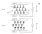
FIGS. 2A-B illustrate diagrams for a marker 200; and
FIG. 3 illustrates a microcapsule 300 for a field modulated dielectric
material; and
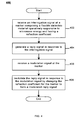
FIG. 4 illustrates a block diagram of a processing logic 400.
DESCRIPTION OF SPECIFIC EMBODIMENTS
FIG. 1 illustrates an EAS system 100. EAS system 100 may comprise
monitoring equipment configured to monitor an interrogation zone, such an
interrogation zone 122. The monitoring equipment may be configured to detect
the presence of a security tag within interrogation zone 122. In one embodiment,
EAS system 100 may include a transmitter 102, a security tag 106, a receiver 116,
a controller 118, an alarm system 120, and a magnetic field generator 124.
Although FIG. 1 shows a limited number of elements, it can be appreciated that
any number of additional elements may be used in system 100. The embodiments
are not limited in this context.
In one embodiment, EAS system 100 may comprise transmitter 102.
Transmitter 102 may comprise any transmitter system configured to transmit an
electromagnetic signal, such as a radio frequency (RF) signal operating in the
microwave range. The microwave signals may include a 2.45 Gigahertz (GHz)
microwave signal or a 915 Megahertz (MHz) microwave signal, for example,
although the embodiments are not limited in this context. Transmitter 102 may
comprise a transmitter antenna operatively coupled to an output stage, which in
turn is connected to a controller, such as controller 118. The output stage may
comprise various conventional driving and amplifying circuits, including a circuit
to generate a high frequency electric current. When the high frequency electric
current is supplied to the transmitter antenna, the transmitter antenna may
generate high frequency electromagnetic signals 104 around the transmitter
antenna. Electromagnetic signals 104 may propagate into interrogation zone 122.
Although electromagnetic signals 104 are described as microwave signals, it may
be appreciated that electromagnetic signals 104 may be any RF signals
appropriately tuned to operate with security tag 106. The embodiments are not
limited in this context.
In one embodiment, EAS system 100 may comprise security tag 106.
Security tag 106 may be designed to attach to an item to be monitored. Examples
of tagged items may include an article of clothing, a Digital Video Disc (DVD) or
Compact Disc (CD) jewel case, a movie rental container, packaging material, and
so forth. The embodiments are not limited in this context.
In one embodiment, security tag 106 may include a marker 108. Marker
108 may comprise, for example, a field modulated dielectric material capable of
operation at microwave frequencies. More particularly, the field modulated
dielectric material of marker 108 may have a reflection coefficient. A reflection
coefficient may represent the ratio of the amplitude of a reflected wave and the
amplitude of an incident wave. The reflected and incident waves may be created,
for example, when electromagnetic signals 104 impinge on marker 108. In one
embodiment, the reflection coefficient of the field modulated dielectric material
may be changed using a low frequency modulation signal, such as modulation
signals 126. Changes in the reflection coefficient may be used to form modulated
reply signals 114, as discussed in further detail with reference to FIGS. 2-4.
In one embodiment, marker 108 may be disposed on or within a security
tag body or housing for security tag 106. The security tag body may be soft or
hard structure designed to support marker 108. Alternatively, the security tag
body may be omitted and marker 108 may comprise the entire security tag 106.
The embodiments are not limited in this context.
In one embodiment, EAS system 100 may comprise a receiver 116.
Receiver 116 may comprise any receiver system configured to receive
electromagnetic signals 104 from transmitter 102, as well as modulated reply
signal 114 from marker 108. For example, receiver 116 may comprise
conventional amplifying and signal-processing circuits, such as band pass filters,
mixers and amplifier circuits. In addition, receiver 116 may comprise an output
stage connected to controller 118, which is configured to receive and process
modulated reply signal 114. The processed signals may then be forwarded to
controller 118 to perform detection operations.
In one embodiment, EAS system 100 may comprise generator 124.
Generator 124 may be configured to generate an electric field or magnetic field
depending on the composition of the field modulated dielectric material selected
to implement marker 108. In one embodiment, for example, generator 124 may
comprise an e-field generator operating in the 1 Hertz to 100 Kilohertz (KHz)
range to form modulations signals 126. In another embodiment, for example,
generator 124 may comprise a coil arrangement to generate a low frequency
alternating current (AC) magnetic field operating in the 1-10 KHz range to form
modulation signals 126. Generator 124 may be configured to generate the electric
field or magnetic field with sufficient strength to cover the same area as
interrogation zone 122.
In one embodiment, EAS system 100 may comprise controller 118.
Controller 118 may comprise a processing and control system configured to
manage various operations for EAS system 100. For example, controller 118 may
send synchronization signals to transmitter 102. Since marker 108 may be
interrogated and detected at a similar frequency used by transmitter 102, the
transmitted signals 104 may interfere with the detection of marker 108.
Therefore, EAS system 100 may be implemented as a "pulsed system," wherein
transmitter 102 and receiver 116 are alternatively turned off and on to reduce
interference at receiver 116. The embodiments are not limited in this context.
In one embodiment, controller 118 may receive processed signals from
receiver 116. Controller 118 may use the processed signals to determine whether
security tag 106 is within interrogation zone 122. For example, modulated reply
signal 114 may include a number of detectable sidebands around the center
frequency. At least one sideband may be used to determine if security tag 106 is
within interrogation zone 122. If security tag 106 is detected within interrogation
zone 122, controller 118 may generate a detect signal and forward the signal to
alarm system 120.
In one embodiment, EAS system 100 may comprise alarm system 120.
Alarm system 120 may comprise any type of alarm system to provide an alarm in
response to an alarm signal. The alarm signal may be received from any number
of EAS components, such as controller 118. Alarm system 120 may comprise a
user interface to program conditions or rules for triggering an alarm. Examples of
the alarm may comprise an audible alarm such as a siren or bell, a visual alarm
such as flashing lights, or a silent alarm. A silent alarm may comprise, for
example, an inaudible alarm such as a message to a monitoring system for a
security company. The message may be sent via a computer network, a telephone
network, a paging network, and so forth. The embodiments are not limited in this
context.
In general operation, transmitter 102 may communicate signals 104 into
interrogation zone 122. Generator 124 may send modulation signals 126 into
interrogation zone 122. Marker 108 may receive signals 104, and transmit a reply
signal at a frequency determined by the product of the two mixing signals as
modulated by the reflection coefficient of marker 108. Modulation signal 126
may cause changes in the reflection coefficient of marker 108, thereby modulating
the reply signal from marker 108 to form modulated reply signal 114. Receiver
116 may receive modulated reply signal 114, process the signal into electrical
current, and forward the processed signal to controller 118. Controller 118 may
receive and analyze the signal from receiver 116 to determine whether security tag
106 is within interrogation zone 122.
In one embodiment, transmitter 110, receiver 116 and controller 118 may
be elements from a conventional EAS system, such as a Digital Microwave
System (DMS) 915 made by Sensormatic® Corporation, as modified using the
principles discussed herein. Different EAS systems, however, may also be
suitable to implement certain embodiments. The embodiments are not limited in
this context.
FIGS. 2A and 2B illustrate a pair of diagrams for a marker 200. Marker
200 may be representative of, for example, marker 108. In one embodiment,
marker 200 may comprise field modulated dielectric material operatively
responsive to RF energy and having a reflection coefficient. Marker 200 may be
configured to receive interrogation signal 104 to cause marker 200 to generate a
reply signal. Marker 200 may also receive modulation signal 126 to change the
reflection coefficient of the field modulated dielectric material in synchrony with
modulation signal 126. The change in reflection coefficient may modulate the
reply signal to form modulated reply signal 114.
In one embodiment, the field modulated dielectric material for marker 200
may comprise a form of electronic paper. Electronic paper may comprise a
display material that has many of the properties of paper. For example, electronic
paper may be used to store an image, may be viewed in reflective light, provides a
relatively wide viewing angle, and is relatively thin and flexible. Unlike
conventional paper, however, electronic paper may be electrically writeable and
erasable. A single sheet of electronic paper may be reused to display different
text, graphics and images under the control of electrical signals.
FIGS. 2A and 2B illustrate marker 200 as implemented using a first form
of electronic paper. In one embodiment, marker 200 may be implemented using a
form of electronic paper similar to a "Gyricon" sheet as developed by the Xerox
Palo Alto Research Center (PARC). A Gyricon sheet may comprise a large
number (e.g., millions) of microspheres 202 embedded within a thin polymer
matrix, such as a transparent plastic 204.
In one embodiment, microspheres 202 may be randomly dispersed
between surfaces 210 and 212, with each microsphere 202 being contained in a
cavity 214. Cavity 214 may comprise an oil-filled cavity to permit each
microsphere 202 to freely rotate within cavity 214. Microspheres 202 may be
"bichromal" with hemispheres being made of material, or coated with material,
having at least two different reflection coefficients. The material selected for each
hemisphere should have a reflection coefficient that provides a relatively high
contrast ratio between the reflection coefficients. The contrast ratio should create
a sufficient difference in the reflection coefficients to create detectable modulation
sidebands observable on the reflected microwave carrier signal. For example, a
first side may comprise a material having a first coefficient that is highly
reflective, such as a metal. A second side may comprise a material having a
second coefficient that is highly absorptive, such as carbon. In a more specific
example, a first side 216 of microsphere 202 may be coated or painted with a
white titanium dioxide, while a second side 218 of microsphere 202 may be
coated or painted with a black carbon. The specific materials and specific
reflection coefficients for a given implementation, however, may vary according
to a number of different factors, such as the operating frequencies of the EAS
system, the area of the interrogation zone, detection distance, and so forth. The
embodiments are not limited in this context.
In one embodiment, microspheres 202 may be rotated by applying an
electric field. Microspheres 202 may be charged so they exhibit an electrical
dipole. When an electric field is applied to microspheres 202 via corresponding
conductors, microspheres 202 may be rotated to present one or the other side to
surfaces 210 or 212, respectively. As shown in FIG. 2A, when a first electric field
is applied to microspheres 202 they may rotate in a first direction 206 to display
the white color having a first reflection coefficient on first side 216 towards
surface 210. The position of microspheres 202 may persist until a second electric
field is applied to microspheres 202. As shown in FIG. 2B, when the second
electric field is applied to microspheres 202 they may rotate in a second direction
208 to display the black color having a second reflection coefficient on second
side 218 toward surface 212.
In one embodiment, modulation signal 126 may be used to control the
rotation of microspheres 202 of marker 200. The rotation of microspheres 202
may change the optical reflection coefficient of the field modulated dielectric
material. Consequently, as signals 104 reflect off of surface 210 and/or surface
212 of marker 200, the changing reflection coefficient may create a modulation
sideband around the reflected microwave carrier signal to form modulated reply
signal 114. Accordingly, modulated reply signal 114 may be used to detect the
presence of marker 200 within interrogation zone 122.
FIG. 3 illustrates a microcapsule to implement marker 200 using a second
form of electronic paper. In one embodiment, marker 200 may be implemented
using a form of electronic paper similar to an "electrophoretic ink" or "e-ink"
sheet as developed by E Ink Corporation. An e-ink sheet is similar in concept to a
Gyricon sheet except the e-ink sheet uses non-rotating spheres. Instead, an e-ink
sheet may comprise transparent polymer microcapsules 300 containing positively
and negatively charged microparticles that each comprise, or are coated, with
material having reflection coefficients with a high contrast ratio. For example,
positively charged microparticles 302 may comprise white titanium dioxide and
negatively charged microparticles 304 may comprise a blue liquid dye.
Movement of the microparticles is controlled using electrophoresis, which is the
movement imparted by an electric field to charged particles that are suspended in
a liquid. When a first electric field is applied to electrodes positioned on the top
and bottom of the microcapsules, positively charged particles 302 migrate to the
positive electrode in direction 310 and negatively charged particles 304 migrate to
the negative electrode in direction 312 thereby displaying the white color
microparticles 302 having a first reflection coefficient on a first side 306 of
microcapsule 300 and the black color microparticles 304 having a second
reflection coefficient on a second side 308 of microcapsule 300. When a second
electric field is applied to the electrodes, the reverse occurs, and the positively
charged particles 302 migrate to the negative electrode in direction 312 and
negatively charged particles 304 migrate to the positive electrode in direction 310
thereby displaying the black color microparticles 304 on first side 306 of
microcapsule 300 and the white color microparticles 302 on second side 308 of
microcapsule 300.
In one embodiment, modulation signal 126 may be used to control the
migration of electrically charged particles of microcapsule 300 for marker 200.
The migration of microparticles may change the optical reflection coefficient of
the field modulated dielectric material. Consequently, as signals 104 reflect off of
surface 210 and/or surface 212 of marker 200, the changing reflection coefficient
may create a modulation sideband around the reflected microwave carrier signal
to form modulated reply signal 114. Accordingly, modulated reply signal 114
may be used to detect the presence of marker 200 within interrogation zone 122.
Operations for the above system 100 and marker 200 may be further
described with reference to the following figures and accompanying examples.
Some of the figures may include programming logic. Although such figures
presented herein may include a particular programming logic, it can be
appreciated that the programming logic merely provides an example of how the
general functionality described herein can be implemented. Further, the given
programming logic does not necessarily have to be executed in the order
presented unless otherwise indicated. In addition, although the given
programming logic may be described herein as being implemented in the above-referenced
modules, it can be appreciated that the programming logic may be
implemented anywhere within the system and still fall within the scope of the
embodiments.
FIG. 4 illustrates a block diagram for a programming logic 400. FIG. 4
illustrates a programming logic 400 that may be representative of the operations
executed by one or more systems described herein, such as system 100 and/or
marker 200. As shown in programming logic 400, an interrogation signal may be
received at a marker comprising a field modulated dielectric material operatively
responsive to microwave energy and having a reflection coefficient at block 402.
A reply signal may be generated in response to the interrogation signal at block
404. A modulation signal may be received at the marker at block 406. The reply
signal may be modulated in response to the modulation signal by changing the
reflection coefficient for the marker to form a modulated reply signal at block
408.
In one embodiment, the modulation signal creates a first electric field, and
the modulating comprises rotating a plurality of microspheres within the field
modulated dielectric material in a first direction to display a first reflection
coefficient on a first side in response to the first electric field. In one
embodiment, the modulation signal creates a second electric field, and the
modulating comprises rotating the plurality of microspheres in a second direction
to display a second reflection coefficient on a second side in response to the
second electric field. The first reflection coefficient and second reflection
coefficient may modulate the reply signal to form the modulated reply signal.
In one embodiment, the modulation signal may cause the marker to create
a first electric field, and the modulating comprises moving positively charged
microparticles to a positive electrode of a microcapsule and negatively charged
microparticles to a negative electrode of the microcapsule to display a first
reflection coefficient on a first side of the microcapsule and a second reflection
coefficient on a second side of the microcapsule in response to the first electric
field. In one embodiment, the modulation signal may cause the marker to create a
second electric field, and the modulating comprises moving the positively charged
microparticles to the negative electrode and the negatively charged microparticles
to the positive electrode to display the second reflection coefficient on the first
side and the first reflection coefficient on the second side in response to the
second electric field. The first reflection coefficient and second reflection
coefficient may modulate the reply signal to form the modulated reply signal.
In the case where modulation is performed using an electric field, there
may be several ways to provide coupling of the external modulating field into the
field modulated dielectric material. Electrodes could be printed in rows and
columns in a screen pattern either single-sided or on both sides of the field
modulated dielectric material. Alternatively, a spiral inductor pattern might be
used if the modulating field occurred at the Radio-Frequency (RF) range, such as
8 to 15 MHz. The electric field would exist between the turns of the inductor.
In the case where modulation is performed using a magnetic field, there
would be no need for a printed conductor pattern. In this case, the film alone
would provide all the required properties for detection.
In one embodiment, the principles discussed herein may be applied in a
Radio-Frequency Identification (RFID) system. For example, an RFID chip may
be connected to a spiral inductor and receive its power from an external RF field
operating at approximately 13.56 MHz, for example. The RFID chip would then
modulate the microwave properties of the material to provide a coded signal over
a relatively long range.
Numerous specific details have been set forth herein to provide a thorough
understanding of the embodiments. It will be understood by those skilled in the
art, however, that the embodiments may be practiced without these specific
details. In other instances, well-known operations, components and circuits have
not been described in detail so as not to obscure the embodiments. It can be
appreciated that the specific structural and functional details disclosed herein may
be representative and do not necessarily limit the scope of the embodiments.
It is worthy to note that any reference to "one embodiment" or "an
embodiment" means that a particular feature, structure, or characteristic described
in connection with the embodiment is included in at least one embodiment. The
appearances of the phrase "in one embodiment" in various places in the
specification are not necessarily all referring to the same embodiment.
All or portions of an embodiment may be implemented using an
architecture that may vary in accordance with any number of factors, such as
desired computational rate, power levels, heat tolerances, processing cycle budget,
input data rates, output data rates, memory resources, data bus speeds and other
performance constraints. For example, an embodiment may be implemented
using software executed by a processor. In another example, an embodiment may
be implemented as dedicated hardware, such as a circuit, an application specific
integrated circuit (ASIC), Programmable Logic Device (PLD) or digital signal
processor (DSP), and so forth. In yet another example, an embodiment may be
implemented by any combination of programmed general-purpose computer
components and custom hardware components. The embodiments are not limited
in this context.