EP1596320B1 - Radio communication system, device and method - Google Patents
Radio communication system, device and method Download PDFInfo
- Publication number
- EP1596320B1 EP1596320B1 EP05252825A EP05252825A EP1596320B1 EP 1596320 B1 EP1596320 B1 EP 1596320B1 EP 05252825 A EP05252825 A EP 05252825A EP 05252825 A EP05252825 A EP 05252825A EP 1596320 B1 EP1596320 B1 EP 1596320B1
- Authority
- EP
- European Patent Office
- Prior art keywords
- primary
- radio communication
- transmission data
- frequency
- modulation
- Prior art date
- Legal status (The legal status is an assumption and is not a legal conclusion. Google has not performed a legal analysis and makes no representation as to the accuracy of the status listed.)
- Expired - Fee Related
Links
Images


Classifications
-
- G—PHYSICS
- G06—COMPUTING; CALCULATING OR COUNTING
- G06K—GRAPHICAL DATA READING; PRESENTATION OF DATA; RECORD CARRIERS; HANDLING RECORD CARRIERS
- G06K7/00—Methods or arrangements for sensing record carriers, e.g. for reading patterns
- G06K7/0008—General problems related to the reading of electronic memory record carriers, independent of its reading method, e.g. power transfer
-
- F—MECHANICAL ENGINEERING; LIGHTING; HEATING; WEAPONS; BLASTING
- F16—ENGINEERING ELEMENTS AND UNITS; GENERAL MEASURES FOR PRODUCING AND MAINTAINING EFFECTIVE FUNCTIONING OF MACHINES OR INSTALLATIONS; THERMAL INSULATION IN GENERAL
- F16L—PIPES; JOINTS OR FITTINGS FOR PIPES; SUPPORTS FOR PIPES, CABLES OR PROTECTIVE TUBING; MEANS FOR THERMAL INSULATION IN GENERAL
- F16L25/00—Constructive types of pipe joints not provided for in groups F16L13/00 - F16L23/00 ; Details of pipe joints not otherwise provided for, e.g. electrically conducting or insulating means
- F16L25/0036—Joints for corrugated pipes
-
- F—MECHANICAL ENGINEERING; LIGHTING; HEATING; WEAPONS; BLASTING
- F16—ENGINEERING ELEMENTS AND UNITS; GENERAL MEASURES FOR PRODUCING AND MAINTAINING EFFECTIVE FUNCTIONING OF MACHINES OR INSTALLATIONS; THERMAL INSULATION IN GENERAL
- F16L—PIPES; JOINTS OR FITTINGS FOR PIPES; SUPPORTS FOR PIPES, CABLES OR PROTECTIVE TUBING; MEANS FOR THERMAL INSULATION IN GENERAL
- F16L21/00—Joints with sleeve or socket
- F16L21/06—Joints with sleeve or socket with a divided sleeve or ring clamping around the pipe-ends
- F16L21/065—Joints with sleeve or socket with a divided sleeve or ring clamping around the pipe-ends tightened by tangentially-arranged threaded pins
-
- G—PHYSICS
- G01—MEASURING; TESTING
- G01S—RADIO DIRECTION-FINDING; RADIO NAVIGATION; DETERMINING DISTANCE OR VELOCITY BY USE OF RADIO WAVES; LOCATING OR PRESENCE-DETECTING BY USE OF THE REFLECTION OR RERADIATION OF RADIO WAVES; ANALOGOUS ARRANGEMENTS USING OTHER WAVES
- G01S13/00—Systems using the reflection or reradiation of radio waves, e.g. radar systems; Analogous systems using reflection or reradiation of waves whose nature or wavelength is irrelevant or unspecified
- G01S13/74—Systems using reradiation of radio waves, e.g. secondary radar systems; Analogous systems
- G01S13/75—Systems using reradiation of radio waves, e.g. secondary radar systems; Analogous systems using transponders powered from received waves, e.g. using passive transponders, or using passive reflectors
- G01S13/751—Systems using reradiation of radio waves, e.g. secondary radar systems; Analogous systems using transponders powered from received waves, e.g. using passive transponders, or using passive reflectors wherein the responder or reflector radiates a coded signal
- G01S13/758—Systems using reradiation of radio waves, e.g. secondary radar systems; Analogous systems using transponders powered from received waves, e.g. using passive transponders, or using passive reflectors wherein the responder or reflector radiates a coded signal using a signal generator powered by the interrogation signal
-
- G—PHYSICS
- G06—COMPUTING; CALCULATING OR COUNTING
- G06K—GRAPHICAL DATA READING; PRESENTATION OF DATA; RECORD CARRIERS; HANDLING RECORD CARRIERS
- G06K19/00—Record carriers for use with machines and with at least a part designed to carry digital markings
- G06K19/06—Record carriers for use with machines and with at least a part designed to carry digital markings characterised by the kind of the digital marking, e.g. shape, nature, code
- G06K19/067—Record carriers with conductive marks, printed circuits or semiconductor circuit elements, e.g. credit or identity cards also with resonating or responding marks without active components
- G06K19/07—Record carriers with conductive marks, printed circuits or semiconductor circuit elements, e.g. credit or identity cards also with resonating or responding marks without active components with integrated circuit chips
- G06K19/0723—Record carriers with conductive marks, printed circuits or semiconductor circuit elements, e.g. credit or identity cards also with resonating or responding marks without active components with integrated circuit chips the record carrier comprising an arrangement for non-contact communication, e.g. wireless communication circuits on transponder cards, non-contact smart cards or RFIDs
-
- H—ELECTRICITY
- H04—ELECTRIC COMMUNICATION TECHNIQUE
- H04L—TRANSMISSION OF DIGITAL INFORMATION, e.g. TELEGRAPHIC COMMUNICATION
- H04L5/00—Arrangements affording multiple use of the transmission path
- H04L5/14—Two-way operation using the same type of signal, i.e. duplex
- H04L5/143—Two-way operation using the same type of signal, i.e. duplex for modulated signals
Definitions
- the present invention relates to a radio communication system, a radio communication device, and a radio communication method of a radio wave communication system using microwaves.
- Illustrative embodiments of the present invention relate to a radio communication system, a radio communication device, and a radio communication method for realizing communication operation with low power consumption between devices at a relatively short distance.
- illustrative embodiments of the present invention relate to a radio communication system, a radio communication device, and a radio communication method that perform data communication by a backscatter system using transmission of an unmodulated carrier from a reading device side, and absorption and reflection of the received radio wave on the basis of an operation of terminating an antenna on a transmitting device side, and particularly to a radio communication system, a radio communication device, and a radio communication method that eliminate or at least reduce effects of transmitter noise on the reading device side to improve reception sensitivity and increase a communication distance.
- RFID is a system including a tag and a reader, in which system the reader reads information stored in the tag in a non-contact manner. While the system is also referred to as an "ID system,” a “data carrier system” and the like, a universally common name for the system is an RFID system.
- the RFID system may be abbreviated to RFID.
- the RFID system is an "identification system using high frequencies (radio waves).”
- Methods of communication between a tag and a reader/writer include for example an electromagnetic coupling type, an electromagnetic induction type, and a radio frequency communication type (see for example, Klaus Finkenzeller (Translated from the 3rd German edition by Rachel Waddington, Swadlincote, UK) "Fundamentals and Applications in Contactless Smart Cards and Identification” (Wiley & Sons LTD ))
- An RFID tag is a device including unique identifying information, and has an operation characteristic of oscillating a radio wave at a modulation frequency corresponding to the identifying information in response to reception of a radio wave of a specific frequency. On the basis of the oscillation frequency of the RFID tag, a reading device side can identify the RFID tag. Hence, a system using RFID makes it possible to identify an article, an owner, and the like using a unique ID written in the RFID tag.
- the RFID system is now used in many systems including for example a system for monitoring the entering and leaving of a room, an article identifying system in distribution, a bill payment system in restaurants and the like, and a system for preventing takeout before payment in stores selling CDs, software and the like.
- a radio identification device of a small size can be produced by packaging an IC chip having a transmission and reception function and a memory function, a source for driving the chip, and an antenna (see for example, Japanese Patent Laid-Open No. Hei 6-123773 ). According to this radio identification device, it is possible to transmit various data on an article or the like to receiving means of the IC chip via the antenna and store the output in a memory, and also read the data in the memory and supply the data to the outside by radio via the antenna as required. Hence, the presence and position of the article or the like can be checked and traced quickly and easily.
- An RFID system includes an RFID tag and a tag reader.
- the tag receives an unmodulated wave f o transmitted from the tag reader, the unmodulated wave f o is rectified and converted into direct-current power, and the direct-current power can be used as operating power of the tag.
- the tag side performs an operation of terminating an antenna according to a bit image of transmission data, and thus uses absorption and reflection of the received radio wave to represent the data. Specifically, when data is 1, the tag terminates the antenna by an antenna impedance to absorb the radio wave from the tag reader. When data is 0, the tag reflects the radio wave from the tag reader by setting a terminal of the antenna in an open state.
- a signal of the same frequency as that of the signal transmitted from the tag reader is returned by the reflection of a backscatter system.
- a communication method of representing data by a pattern of absorption and reflection of the thus arrived radio wave is referred to as a "backscatter system.”
- the tag can transmit information therewithin to the reader side without a power supply.
- a radio communication system of the backscatter system is limited in communication range to a relatively short distance, and is thus often applied to identification and authentication of an article, a person and the like, as is typified by the RFID tag.
- the RFID tag generally has no power supply, and is supplied with power from the radio wave from the reader. This power is supplied from a battery within the device, whereby radio data transmission with low power consumption by the backscatter system can be realized. That is, when a communication distance is limited, radio communication of the backscatter system has a characteristic of being able to establish a radio transmission line with a very low power consumption.
- radio communication of the backscatter system has a characteristic of being able to establish a radio transmission line with a very low power consumption.
- the communication system based on the backscatter system performs data communication using absorption and reflection of the received radio wave on the basis of the operation of terminating the antenna as a fundamental operation.
- frequency of a carrier from the reader and center frequency of the reflected wave are the same, and the reader side performs transmission and reception at the same frequency.
- a receiving unit is affected by the transmission frequency that goes around into the receiving unit from a transmitting side, and needs to process the reflected wave having a weak power. That is, the receiving unit is easily affected by a DC offset and transmitter noise, thus making it difficult to increase a transmission distance.
- a modulation system in the backscatter system is generally an ASK modulation system or a PSK modulation system in most cases, thus making it difficult to increase speed.
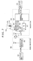
- FIG. 7 shows an example of configuration of a radio communication system of a previously proposed backscatter system.
- Reference numeral 500 denotes a radio transmission device on a mobile device side.
- Reference numeral 510 denotes a radio transmission and reception device on a reader side. Suppose that data transmission is performed by the backscatter system from the radio transmission device 500 to the radio transmission and reception device 510.
- the radio transmission device 500 is connected to an application unit 503 such as a digital camera or the like.
- the radio transmission and reception device 510 is connected to an application unit 519 such as a printer or the like.
- the radio transmission and reception device 510 includes an antenna 511, a circulator 512 for separating a transmitting wave and a received wave from each other, a receiving unit 514, a local oscillator 513 shared for transmission and reception by the receiving unit 514 and a transmitting unit 517, and a baseband processing unit 518.
- the receiving unit 514 and the transmitting unit 517 both use a direct conversion system.
- the receiving unit 514 includes a quadrature demodulation unit 515 and an AGC amplifier 516.
- An unmodulated carrier is transmitted to the radio transmission device 500 by turning on the transmitting unit 517 by the baseband processing unit 518 and thereby transmitting frequency f o of the local oscillator 513 from the antenna 511 via the circulator 512.
- the transmitted unmodulated carrier f o reaches the radio transmission device 500.
- the radio transmission device 500 includes an antenna 501 and a backscatter modulator 502.
- the backscatter modulator 502 performs backscatter ASK, PSK, or QPSK modulation according to transmission data of the application unit 503.
- the modulation can be easily performed by on/off operation of a diode, a GaAs switch or the like.
- a modulated wave eventually reflected from the antenna 501 is generated with the center frequency f o of the unmodulated carrier as a center.
- the backscattered modulated wave having the center frequency f o is received by the antenna 511, the circulator 512, and the receiving unit 514.
- the quadrature demodulation unit 515 is supplied with the frequency f o of the local oscillator 513, performs direct conversion reception, and generates an I' signal and a Q' signal of a baseband signal.
- the I' signal and the Q' signal of the baseband signal are amplified to a desired level by the AGC amplifier 516 in a succeeding stage. Thereby an I signal and a Q signal of the baseband signal are obtained.
- the I signal and the Q signal of the baseband signal are supplied to the baseband processing unit 518.
- the baseband processing unit 518 performs demodulation, and then supplies received data and a received clock to the application unit 519.
- the unmodulated carrier f o from the transmitting unit 517 is emitted from the antenna 511 via the circulator 512, and also goes around into the receiving unit 514 side.
- This component going around into the receiving unit 514 side can be reduced to a degree by the circulator 512.
- a value of the reduction is not infinite, and an isolation of about 20 dB is an actual value.
- FIG. 7 also shows a frequency spectrum on the reader side.
- Reference numeral 520 denotes a frequency spectrum at an input terminal of the quadrature demodulation unit 515.
- Reference numeral 522 denotes the modulated wave reflected by backscatter, for example a BPSK modulated wave.
- Reference numeral 521 denotes the unmodulated carrier. When the modulated signal 522 is small, the unmodulated carrier 521 has a larger value.
- This unmodulated carrier f o enters the quadrature demodulation unit 515 to be mixed with the local frequency f o of the local oscillator 513. Consequently a high direct-current voltage is generated. This forms a DC offset, which produces a great adverse effect on operation of the quadrature demodulation unit 515. Thus, the very small modulated signal becomes distorted to be difficult to demodulate, thereby constituting a major cause of an impediment to increasing a transmission distance.
- FIG. 5 shows an example of configuration of an RFID system in which a tag side shifts reception frequency f o by a predetermined center frequency f s in one of a positive direction and a negative direction, and returns a reflected wave.
- Reference numeral 100 denotes a radio transmission device on a mobile device side.
- Reference numeral 110 denotes a radio transmission and reception device on a reader side.
- the radio transmission device 100 is connected to an application unit 105 such as a digital camera or the like.
- the radio transmission and reception device 110 is connected to an application unit 119 such as a printer or the like.
- the radio transmission and reception device 110 includes an antenna 111, a circulator 112 for separating a transmitting wave and a received wave from each other, a receiving unit 114, a local oscillator 115 for the receiving unit 114, a transmitting unit 116, a local oscillator 117 for the transmitting unit 116, and a baseband processing unit 118.
- the receiving unit 114 and the transmitting unit 116 both use a direct conversion system.
- An unmodulated carrier is transmitted to the radio transmission device 100 by turning on the transmitting unit 116 by the baseband processing unit 118 and transmitting frequency f o of the local oscillator 117 from the antenna 111 via a band-pass filter 113 and the circulator 112.
- the transmitted unmodulated carrier f o reaches the radio transmission device 100.
- the band-pass filter 113 is provided to reduce effects of transmitter noise on the receiving unit 114.
- the radio transmission device 100 includes an antenna 101, a backscatter modulator 102, a subcarrier QPSK modulator 103, and a subcarrier oscillator 104.
- the subcarrier QPSK modulator 103 performs QPSK modulation at a subcarrier frequency f s .
- Data to be subjected to the QPSK modulation is received from the application unit 105 as transmission data (TXDATA) and a transmission clock (TXCLK).
- QPSK modulation requires a 90° phase shifter.
- the 90° phase shifter can be easily created from a clock of four times f s .
- an analog delay line may be used.
- a generated QPSK modulated wave having a center frequency f s is subjected to ASK modulation by the backscatter modulator 102.
- the backscatter modulation can be easily performed by using a diode, a GaAs switch or the like (known).
- the QPSK modulated wave eventually reflected from the antenna 101 is generated in both sidebands of the frequency f o of the unmodulated carrier, that is, two bands of center frequencies f o + f s and f o - f s .
- f o + f s of the modulated wave divided into both sidebands is used.
- the modulated wave of f o - f s can be removed by using a band-pass filter 106 inserted between the antenna 101 and the backscatter modulator 102, for example.
- a loss from insertion of the band-pass filter 106 occurs twice, causing a decrease in reflection efficiency.
- the insertion of the band-pass filter 106 increases device cost.
- the backscattered modulated wave of f o + f s is received by the antenna 111, the circulator 112, and the receiving unit 114.
- the receiving unit 114 performs direct conversion reception at the frequency f o + f s of the local oscillator 115.
- the QPSK modulated wave is converted into baseband signals I and Q.
- the baseband signals I and Q are sent to the baseband processing unit 118.
- the baseband processing unit 118 performs QPSK demodulation processing (carrier synchronization and symbol synchronization), thereby generates received data RXDATA and a received clock RXCLK, and then supplies the received data RXDATA and the received clock RXCLK to the application unit 119.
- QPSK demodulation processing carrier synchronization and symbol synchronization
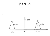
- FIG. 6 shows a spectrum of the reflected wave in the RFID system shown in FIG. 5 .
- the backscatter modulation system is ASK.
- Reference numeral 200 denotes a returned component of the unmodulated carrier of the frequency f o transmitted from the radio transmission and reception device 110.
- Reference numeral 201 denotes the QPSK modulated wave of the center frequency f o + f s .
- Reference numeral 202 denotes the QPSK modulated wave of the center frequency f o - f s .
- the unmodulated carrier transmitted from the radio transmission and reception device 110 is divided into the components 200, 201, and 202 and then reflected. Therefore the modulated signal on one side has a low level. That is, the level of the originally very weak reflected wave is further lowered, which is one cause of decrease in communication distance.
- EP 0 779 520 A2 describes a Frequency Division Multiple (FDMA) duplex radio communication system.
- FDMA Frequency Division Multiple
- US 2002/0142747 A1 describes a frequency conversion circuit.
- US 5,861,781 describes a single sideband double quadrature modulator.
- a radio communication system for performing data communication by a backscatter system, using absorption and reflection of a received radio wave according to claim 6.
- the system herein refers to a logical set of a plurality of apparatuses (or functional modules for realizing specific functions) regardless of whether each apparatus or functional module is present within the same casing.
- the radio communication system is applicable to an RFID system in which a tag can perform data communication without a power supply by the backscatter system.
- the data transmitting device corresponds to a tag
- the data reading device corresponds to a tag reader.
- frequency of a carrier from a reader and center frequency of a reflected wave are the same, and since the reader side performs transmission and reception at the same frequency, a receiving unit of the tag reader needs to process the reflected wave having a weak power while being affected by a DC offset and transmitter noise.
- the radio communication system eliminates or at least reduces effects of a DC offset and transmitter noise on the tag reader side by shifting the unmodulated carrier of the frequency f o from the tag reader side by f s on the tag side and then returning the reflected wave.
- the reflected modulated wave appears in a state of being divided into both sidebands shifted by the subcarrier frequency to a plus side and a minus side from a center of the unmodulated carrier.
- the data transmitting device subjects transmission data to primary modulation with a center frequency fs, and performs secondary modulation by multiplying a signal resulting from the primary modulation by the unmodulated carrier.
- the data transmitting device generates a modulated signal of a reflected wave in which one of frequencies fo + fs and fo - fs is suppressed, and then transmits the modulated signal of the reflected wave. It is therefore possible to improve reflection efficiency and prevent or at least reduce a power loss of the reflected wave, and thus improve reception sensitivity and increase transmission distance.
- a reflected wave on one side of two divided sidebands does not need to be removed by a filter, an increase in cost can be prevented.
- the data transmitting device subjects transmission data to primary modulation by one of a BPSK system and a QPSK system using a center frequency fs.
- the data transmitting device thereby generates primary modulated transmission data I.
- the data transmitting device generates primary modulated transmission data Q by giving a phase difference of 90 degrees to the primary modulated transmission data I.
- the data transmitting device generates a modulated signal of a reflected wave in which one of frequencies fo + fs and fo - fs is suppressed by multiplying the primary modulated transmission data by an I and a Q of the unmodulated carrier for quadrature modulation by the backscatter system.
- the reflected modulated wave of one of the frequencies fo + fs and fo - fs can be selectively generated by changing a combination in which the inputs I and Q of the unmodulated carrier for quadrature modulation and the primary modulated transmission data I and Q resulting from the primary modulation are multiplied together.
- a reflected wave of a frequency fo - fs can be returned to the data reading device.
- a reflected wave of a frequency fo + fs can be returned to the data reading device.
- the data transmitting device may change the center frequency fs for the primary modulation.
- a radio communication system it is possible to provide a radio communication system, a radio communication device, and a radio communication method that are excellent in making it possible to improve reception sensitivity and increase communication distance by separating transmission frequency on a reading device side from reception frequency returned as a reflected wave from a transmitting device side.
- a radio communication system a radio communication device, and a radio communication method that are excellent in eliminating or at least reducing effects of a DC offset and transmitter noise on the tag reader side to improve the reception sensitivity and increase the communication distance by shifting an unmodulated carrier of frequency f o from the tag reader side by f s on the tag side and returning a reflected wave.
- a radio communication system a radio communication device, and a radio communication method that are excellent in making it possible to improve the reception sensitivity and increase the communication distance by improving reflection efficiency and preventing or at least reducing a power loss of the reflected wave when shifting the unmodulated carrier of frequency f o from the tag reader side by f s on the tag side and returning the reflected wave.
- the tag reader side since the tag reader side does not need to remove a reflected wave on one side of two divided sidebands by a filter, an increase in cost can be prevented.
- Embodiments of the present invention relate to an RFID system in which a tag can perform data communication without a power supply by a backscatter system.
- frequency of a carrier from a reader and center frequency of a reflected wave are the same, and since the reader side performs transmission and reception at the same frequency, a receiving unit of the tag reader is affected by a DC offset and transmitter noise.
- a radio communication system eliminates or at least reduces effects of a DC offset and transmitter noise on a tag reader side by shifting an unmodulated carrier of a frequency f o from the tag reader side by f s on a tag side and then returning a reflected wave.
- FIG. 1 schematically shows a configuration of a radio communication device according to one embodiment of the present invention.
- the radio communication device shown in the figure corresponds to a tag in an RFID system.
- the radio communication device receives an unmodulated carrier of a frequency f o transmitted from a tag reader, and shifts the carrier by a frequency f s by a backscatter system.
- the radio communication device generates a modulated signal of a reflected wave in which one of both sidebands f o + f s and f o - f s is suppressed, and then transmits the modulated signal.
- the radio communication device includes a frequency generating unit 11, a primary modulating unit 12, and a secondary modulating unit 13.
- the frequency generating unit 11 generates a center frequency f s for primary modulation.
- the frequency generating unit 11 may change the center frequency f s for primary modulation.
- the primary modulating unit 12 subjects transmission data to primary modulation by a BPSK or a QPSK system using the center frequency f s .
- the primary modulating unit 12 thereby generates an I-axis signal of the transmission data.
- the primary modulating unit 12 generates a Q-axis signal of the transmission data by giving a phase difference of 90 degrees to the I-axis signal of the transmission data.
- the secondary modulating unit 13 subjects the primary modulated transmission data to secondary modulation.
- the secondary modulating unit in the present embodiment is formed by a quadrature modulator for quadrature modulation of the unmodulated carrier of the frequency f o transmitted from the tag reader by the backscatter system. That is, the secondary modulating unit 13 multiplies an I-axis signal and a Q-axis signal of the unmodulated carrier input thereto by the I-axis signal and the Q-axis signal of the above-described primary modulated transmission data, respectively.
- FIG. 2 shows a modification of the radio communication device as an RFID tag shown in FIG. 1 .
- the radio communication device shown in the figure further includes a switching unit 14.
- the switching unit 14 changes a combination in which an I-axis signal and a Q-axis signal of an unmodulated carrier and an I-axis signal and a Q-axis signal of primary modulated transmission data as described above are multiplied together.
- a reflected wave signal of a frequency f o - f s can be returned to the tag reader.
- a reflected wave signal of a frequency f o + f s can be returned to the tag reader.
- FIG. 3 shows a concrete configuration of a radio communication device according to an embodiment of the present invention.
- the radio communication device shown in the figure operates as a tag in an RFID system, and is capable of QPSK radio communication by the backscatter system with reflection efficiency improved and an unwanted spectrum suppressed.
- This radio communication device is characterized in that an image rejection type backscatter modulator is used to extract a frequency component on only one side of a modulated wave.
- Reference numeral 300 denotes an image rejection type backscatter modulator.
- This backscatter modulator 300 includes an antenna 301, a splitter/synthesizer 302, high-frequency switches 303 and 305, and a ⁇ /8 phase shifter 304.
- the high-frequency switches 303 and 305 are formed by a diode, a GaAs switch or the like
- the phase shifter 304 is formed by a strip line or the like.
- the parts indicated by reference numerals 301 to 305 form a quadrature modulation unit.
- a signal received by the antenna 301 is branched into two signals by the splitter/synthesizer 302.
- One high-frequency switch 303 is turned on to terminate the antenna 301 by an antenna impedance and thus absorb the radio wave from a tag reader, and the switch is turned off to reflect the radio wave from the tag reader. That is, the high-frequency switch 303 creates total reflection in an open state and a short state according to data, and thus operates as a BPSK modulator with a phase difference of 180 degrees.
- the other high-frequency switch 305 similarly absorbs or reflects the radio wave from the tag reader by being turned on/off. However, since the lambda ⁇ /8 phase shifter 304 is inserted at an intermediate point, the high-frequency switch 305 operates as a BPSK modulator advanced in phase in both ways by a total of lambda ⁇ /4, that is, 90°.
- the two high-frequency switches 303 and 305 and the phase shifter 304 can form a backscatter type quadrature modulator.
- a signal controlled by the high-frequency switch 303 is an I-axis signal and that a signal controlled by the high-frequency switch 305 is a Q-axis signal.
- Primary modulated transmission data is given to the I and the Q to thereby form a backscatter type QPSK modulator.
- a shift of frequency of the reflected wave cannot be realized. Therefore a function of shifting the frequency by f s is required.
- Reference numerals 306 to 311 in FIG. 3 generate an I-axis signal and a Q-axis signal of primary modulated transmission data for shifting the frequency by f s .
- a S/P converter unit 309 subjects transmission data (TX DATA) and a transmission clock (TX CLK) to a serial-to-parallel conversion including Gray coding.
- TX DATA transmission data
- TX CLK transmission clock
- the output is P1 and P2.
- a shift clock oscillator 310 is required to shift the frequency by f s . This oscillator oscillates at f s or four times f s . An output of the shift clock oscillator 310 is divided into two signals of 0° and 90° in a 90° phase shifter 308.
- the 90° phase shifter 308 can be easily created from a clock of four times f s when the 90° phase shifter 308 is formed by a digital circuit. Also, an analog delay line may be used without use of a clock of four times f s .
- the two signals different from each other in phase by 90° are input to a QPSK modulator 306.
- the QPSK modulator 306 generates for example four signals of f s different from each other in phase by 90° from the two signals from the phase shifter 308.
- the QPSK modulator 306 generates a digital QPSK signal by selecting the four signals according to the transmission data P1 and P2. Let this digital QPSK signal be an I-axis signal 312. Further, let a Q-axis signal 313 be a signal obtained by delaying the phase of the I-axis signal 312 by 90° by a 90° phase shifter 307.
- the modulation system of the QPSK modulator 306 is controlled by a modulation switching signal (MOD CONT) 314 so that switching can be performed between modulation systems QPSK and BPSK.
- MOD CONT modulation switching signal
- MOD CONT 0 at the time of BPSK modulation
- MOD CONT 1 at the time of QPSK modulation.
- the I-axis signal 312 and the Q-axis signal 313 described above are subjected to backscatter modulation by the above-described quadrature modulation unit. Thereby a spectrum in which one side of QPSK spectra occurring on both sides of a carrier frequency is attenuated can be obtained.
- the modulated wave occurs in both sidebands of f o - f s and f o + f s . It is also indicated that signal level is halved.
- Reference numeral 311 in FIG. 3 denotes a frequency divider.
- the frequency divider 311 divides frequency of the shift clock oscillator 310.
- 1, 2, 4 or the like as a frequency dividing ratio n and using an output signal of the frequency divider for the transmission clock, it is possible to generate an I-axis signal and a Q-axis signal in synchronism at an EXOR output of the 90° phase shifter 307 and the QPSK modulator 306.
- a hazard occurs because a data change point and a clock change point become the same. A measure against this is not directly related to the subject matter of the present invention, and therefore will not be described herein.
- FIG. 4 shows a spectrum of the thus generated reflected wave.
- Reference numeral 401 denotes the QPSK modulated wave at a center frequency f o - f s .
- Reference numeral 400 denotes a leakage component of the QPSK modulated wave at a center frequency f o
- reference numeral 402 denotes a leakage component of the QPSK modulated wave at a center frequency f o + f s . Both the components are caused by an imbalance of orthogonality at each of f o and f s , and are not caused ideally.
- the transmitting and receiving device 110 shown in FIG. 5 can be used as it is as the tag reader for receiving and demodulating the above-described f o + f s modulated wave, and therefore description thereof will not be made in order to avoid repetition of the description.
Description
- The present invention relates to a radio communication system, a radio communication device, and a radio communication method of a radio wave communication system using microwaves. Illustrative embodiments of the present invention relate to a radio communication system, a radio communication device, and a radio communication method for realizing communication operation with low power consumption between devices at a relatively short distance.
- More particularly, illustrative embodiments of the present invention relate to a radio communication system, a radio communication device, and a radio communication method that perform data communication by a backscatter system using transmission of an unmodulated carrier from a reading device side, and absorption and reflection of the received radio wave on the basis of an operation of terminating an antenna on a transmitting device side, and particularly to a radio communication system, a radio communication device, and a radio communication method that eliminate or at least reduce effects of transmitter noise on the reading device side to improve reception sensitivity and increase a communication distance.
- One example of radio communication means applicable in only a limited area is RFID. RFID is a system including a tag and a reader, in which system the reader reads information stored in the tag in a non-contact manner. While the system is also referred to as an "ID system," a "data carrier system" and the like, a universally common name for the system is an RFID system. The RFID system may be abbreviated to RFID. Incidentally, the RFID system is an "identification system using high frequencies (radio waves)." Methods of communication between a tag and a reader/writer include for example an electromagnetic coupling type, an electromagnetic induction type, and a radio frequency communication type (see for example, Klaus Finkenzeller (Translated from the 3rd German edition by Rachel Waddington, Swadlincote, UK) "Fundamentals and Applications in Contactless Smart Cards and Identification" (Wiley & Sons LTD))
- An RFID tag is a device including unique identifying information, and has an operation characteristic of oscillating a radio wave at a modulation frequency corresponding to the identifying information in response to reception of a radio wave of a specific frequency. On the basis of the oscillation frequency of the RFID tag, a reading device side can identify the RFID tag. Hence, a system using RFID makes it possible to identify an article, an owner, and the like using a unique ID written in the RFID tag. The RFID system is now used in many systems including for example a system for monitoring the entering and leaving of a room, an article identifying system in distribution, a bill payment system in restaurants and the like, and a system for preventing takeout before payment in stores selling CDs, software and the like.
- A radio identification device of a small size can be produced by packaging an IC chip having a transmission and reception function and a memory function, a source for driving the chip, and an antenna (see for example, Japanese Patent Laid-Open No.
Hei 6-123773 - An RFID system includes an RFID tag and a tag reader. When the tag receives an unmodulated wave fo transmitted from the tag reader, the unmodulated wave fo is rectified and converted into direct-current power, and the direct-current power can be used as operating power of the tag. The tag side performs an operation of terminating an antenna according to a bit image of transmission data, and thus uses absorption and reflection of the received radio wave to represent the data. Specifically, when data is 1, the tag terminates the antenna by an antenna impedance to absorb the radio wave from the tag reader. When data is 0, the tag reflects the radio wave from the tag reader by setting a terminal of the antenna in an open state. A signal of the same frequency as that of the signal transmitted from the tag reader is returned by the reflection of a backscatter system. A communication method of representing data by a pattern of absorption and reflection of the thus arrived radio wave is referred to as a "backscatter system." Thus, the tag can transmit information therewithin to the reader side without a power supply.
- Conventionally, a radio communication system of the backscatter system is limited in communication range to a relatively short distance, and is thus often applied to identification and authentication of an article, a person and the like, as is typified by the RFID tag.
- On the other hand, the RFID tag generally has no power supply, and is supplied with power from the radio wave from the reader. This power is supplied from a battery within the device, whereby radio data transmission with low power consumption by the backscatter system can be realized. That is, when a communication distance is limited, radio communication of the backscatter system has a characteristic of being able to establish a radio transmission line with a very low power consumption. Recently, with improvement of packaging technology, IC chips having a memory function have appeared, and also memories of the IC chips have been increasing in capacity. There is hence a desire to not only communicate relatively short data such as identifying and authenticating information but also adopt the communication of the backscatter system for general data transmission. For example, the communication of the backscatter system is useful in transmitting images from a digital camera or a portable telephone to a PC, a printer, a TV or the like.
- The communication system based on the backscatter system performs data communication using absorption and reflection of the received radio wave on the basis of the operation of terminating the antenna as a fundamental operation. Generally, frequency of a carrier from the reader and center frequency of the reflected wave are the same, and the reader side performs transmission and reception at the same frequency.
- In such a case, a receiving unit is affected by the transmission frequency that goes around into the receiving unit from a transmitting side, and needs to process the reflected wave having a weak power. That is, the receiving unit is easily affected by a DC offset and transmitter noise, thus making it difficult to increase a transmission distance. In addition, a modulation system in the backscatter system is generally an ASK modulation system or a PSK modulation system in most cases, thus making it difficult to increase speed.
-
FIG. 7 shows an example of configuration of a radio communication system of a previously proposed backscatter system. -
Reference numeral 500 denotes a radio transmission device on a mobile device side.Reference numeral 510 denotes a radio transmission and reception device on a reader side. Suppose that data transmission is performed by the backscatter system from theradio transmission device 500 to the radio transmission andreception device 510. - The
radio transmission device 500 is connected to anapplication unit 503 such as a digital camera or the like. Similarly, the radio transmission andreception device 510 is connected to anapplication unit 519 such as a printer or the like. - The radio transmission and
reception device 510 includes anantenna 511, acirculator 512 for separating a transmitting wave and a received wave from each other, areceiving unit 514, alocal oscillator 513 shared for transmission and reception by thereceiving unit 514 and a transmittingunit 517, and abaseband processing unit 518. Suppose in the example shown in the figure that the receivingunit 514 and the transmittingunit 517 both use a direct conversion system. Further, thereceiving unit 514 includes aquadrature demodulation unit 515 and anAGC amplifier 516. An unmodulated carrier is transmitted to theradio transmission device 500 by turning on the transmittingunit 517 by thebaseband processing unit 518 and thereby transmitting frequency fo of thelocal oscillator 513 from theantenna 511 via thecirculator 512. - The transmitted unmodulated carrier fo reaches the
radio transmission device 500. Theradio transmission device 500 includes anantenna 501 and abackscatter modulator 502. Thebackscatter modulator 502 performs backscatter ASK, PSK, or QPSK modulation according to transmission data of theapplication unit 503. The modulation can be easily performed by on/off operation of a diode, a GaAs switch or the like. Thus, a modulated wave eventually reflected from theantenna 501 is generated with the center frequency fo of the unmodulated carrier as a center. - In the radio transmission and
reception device 510, the backscattered modulated wave having the center frequency fo is received by theantenna 511, thecirculator 512, and thereceiving unit 514. Thequadrature demodulation unit 515 is supplied with the frequency fo of thelocal oscillator 513, performs direct conversion reception, and generates an I' signal and a Q' signal of a baseband signal. - The I' signal and the Q' signal of the baseband signal are amplified to a desired level by the
AGC amplifier 516 in a succeeding stage. Thereby an I signal and a Q signal of the baseband signal are obtained. The I signal and the Q signal of the baseband signal are supplied to thebaseband processing unit 518. Thebaseband processing unit 518 performs demodulation, and then supplies received data and a received clock to theapplication unit 519. - The unmodulated carrier fo from the transmitting
unit 517 is emitted from theantenna 511 via thecirculator 512, and also goes around into thereceiving unit 514 side. This component going around into thereceiving unit 514 side can be reduced to a degree by thecirculator 512. However, a value of the reduction is not infinite, and an isolation of about 20 dB is an actual value. -
FIG. 7 also shows a frequency spectrum on the reader side.Reference numeral 520 denotes a frequency spectrum at an input terminal of thequadrature demodulation unit 515.Reference numeral 522 denotes the modulated wave reflected by backscatter, for example a BPSK modulated wave.Reference numeral 521 denotes the unmodulated carrier. When the modulatedsignal 522 is small, theunmodulated carrier 521 has a larger value. - This unmodulated carrier fo enters the
quadrature demodulation unit 515 to be mixed with the local frequency fo of thelocal oscillator 513. Consequently a high direct-current voltage is generated. This forms a DC offset, which produces a great adverse effect on operation of thequadrature demodulation unit 515. Thus, the very small modulated signal becomes distorted to be difficult to demodulate, thereby constituting a major cause of an impediment to increasing a transmission distance. - As one method for solving such a problem, there is a method of shifting reception frequency fo by a predetermined center frequency fs in one of a positive direction and a negative direction, and returning a reflected wave on a tag side. In this case, frequency of the reflected wave received on a tag reader side is not the same as transmission frequency. Therefore effects of a DC offset and transmitter noise are avoided, so that the reflected wave can be received with high sensitivity. Thus a transmission distance can be increased.
- For example, a method of first performing QPSK modulation using a subcarrier and then performing ASK or PSK modulation by the backscatter system as secondary modulation is proposed (see for example, Japanese Patent Laid-Open No.
Hei 10-209914 -
FIG. 5 shows an example of configuration of an RFID system in which a tag side shifts reception frequency fo by a predetermined center frequency fs in one of a positive direction and a negative direction, and returns a reflected wave. -
Reference numeral 100 denotes a radio transmission device on a mobile device side.Reference numeral 110 denotes a radio transmission and reception device on a reader side. Suppose that data transmission is performed by the backscatter system from theradio transmission device 100 to the radio transmission andreception device 110. Theradio transmission device 100 is connected to anapplication unit 105 such as a digital camera or the like. Similarly, the radio transmission andreception device 110 is connected to anapplication unit 119 such as a printer or the like. - The radio transmission and
reception device 110 includes anantenna 111, acirculator 112 for separating a transmitting wave and a received wave from each other, a receivingunit 114, alocal oscillator 115 for the receivingunit 114, a transmittingunit 116, alocal oscillator 117 for the transmittingunit 116, and abaseband processing unit 118. Suppose in this case that the receivingunit 114 and the transmittingunit 116 both use a direct conversion system. - An unmodulated carrier is transmitted to the
radio transmission device 100 by turning on the transmittingunit 116 by thebaseband processing unit 118 and transmitting frequency fo of thelocal oscillator 117 from theantenna 111 via a band-pass filter 113 and thecirculator 112. The transmitted unmodulated carrier fo reaches theradio transmission device 100. The band-pass filter 113 is provided to reduce effects of transmitter noise on the receivingunit 114. - The
radio transmission device 100 includes anantenna 101, abackscatter modulator 102, asubcarrier QPSK modulator 103, and asubcarrier oscillator 104. - The subcarrier QPSK
modulator 103 performs QPSK modulation at a subcarrier frequency fs. Data to be subjected to the QPSK modulation is received from theapplication unit 105 as transmission data (TXDATA) and a transmission clock (TXCLK). - Generally QPSK modulation requires a 90° phase shifter. However, when QPSK modulation is performed by a digital circuit, the 90° phase shifter can be easily created from a clock of four times fs. Also, an analog delay line may be used.
- A generated QPSK modulated wave having a center frequency fs is subjected to ASK modulation by the
backscatter modulator 102. The backscatter modulation can be easily performed by using a diode, a GaAs switch or the like (known). Thus, the QPSK modulated wave eventually reflected from theantenna 101 is generated in both sidebands of the frequency fo of the unmodulated carrier, that is, two bands of center frequencies fo + fs and fo - fs. - In the example shown in
FIG. 5 , fo + fs of the modulated wave divided into both sidebands is used. The modulated wave of fo - fs can be removed by using a band-pass filter 106 inserted between theantenna 101 and thebackscatter modulator 102, for example. However, a loss from insertion of the band-pass filter 106 occurs twice, causing a decrease in reflection efficiency. In addition, the insertion of the band-pass filter 106 increases device cost. - In the radio transmission and
reception device 110, the backscattered modulated wave of fo + fs is received by theantenna 111, thecirculator 112, and the receivingunit 114. - The receiving
unit 114 performs direct conversion reception at the frequency fo + fs of thelocal oscillator 115. The QPSK modulated wave is converted into baseband signals I and Q. The baseband signals I and Q are sent to thebaseband processing unit 118. - The
baseband processing unit 118 performs QPSK demodulation processing (carrier synchronization and symbol synchronization), thereby generates received data RXDATA and a received clock RXCLK, and then supplies the received data RXDATA and the received clock RXCLK to theapplication unit 119. - However, the above-described method of thus shifting the unmodulated carrier of the frequency fo from the tag reader side by fs on the tag side and returning the reflected wave has the following problems.
- (1) The reflected modulated wave appears in a state of being divided into both sidebands shifted by the subcarrier frequency to a plus side and a minus side from a center of the unmodulated carrier from the reader. Since the actually necessary modulated wave is on only one side, the other side needs to be cut off by the filter. However, when the filter is used in the backscatter system, a loss from the insertion of the filter occurs in both ways, causing a decrease in reflection efficiency. In addition, an increase in cost of the filter is a problem.
- (2) Energy of the reflected wave is divided into both sidebands. Thus, when only one side is used, the energy allocated to the unused other side constitutes a power loss, thus causing a decrease in power of the reflected wave. For example, it is considered that the power of the reflected wave is decreased by at least 3 dB. The backscatter system using ASK further increases the decrease.
-
FIG. 6 shows a spectrum of the reflected wave in the RFID system shown inFIG. 5 . Suppose that the backscatter modulation system is ASK. -
Reference numeral 200 denotes a returned component of the unmodulated carrier of the frequency fo transmitted from the radio transmission andreception device 110.Reference numeral 201 denotes the QPSK modulated wave of the center frequency fo + fs.Reference numeral 202 denotes the QPSK modulated wave of the center frequency fo - fs. - As shown in the figure, the unmodulated carrier transmitted from the radio transmission and
reception device 110 is divided into thecomponents - It is desirable to provide a radio communication system, a radio communication device, and a radio communication method that are excellent in suitably performing data communication by a backscatter system using transmission of an unmodulated carrier from a reading device side, and absorption and reflection of the received radio wave on the basis of an operation of terminating an antenna on a transmitting device side.
- It is also desirable to provide a radio communication system, a radio communication device, and a radio communication method that are excellent in eliminating or at least reducing effects of transmitter noise on the reading device side to improve reception sensitivity and increase a communication distance.
- It is also desirable to provide a radio communication system, a radio communication device, and a radio communication method that are excellent in eliminating or at least reducing effects of a DC offset and transmitter noise on the tag reader side to improve the reception sensitivity and increase the communication distance by shifting an unmodulated carrier of frequency fo from the tag reader side by fs on the tag side and returning a reflected wave.
- It is also desirable to provide a radio communication system, a radio communication device, and a radio communication method that are excellent in making it possible to improve the reception sensitivity and increase the communication distance by improving reflection efficiency and preventing or at least reducing a power loss of the reflected wave when shifting the unmodulated carrier of frequency fo from the tag reader side by fs on the tag side and returning the reflected wave.
-
EP 0 779 520 A2 describes a Frequency Division Multiple (FDMA) duplex radio communication system. -
US 2002/0142747 A1 describes a frequency conversion circuit.US 5,861,781 describes a single sideband double quadrature modulator. - The present invention has been made in view of the above problems. Various respective aspects of the present invention are set out in the appended claims.
- According to an embodiment of the present invention, there is provided a radio communication system for performing data communication by a backscatter system, using absorption and reflection of a received radio wave according to claim 6.
- The system herein refers to a logical set of a plurality of apparatuses (or functional modules for realizing specific functions) regardless of whether each apparatus or functional module is present within the same casing.
- The radio communication system according to the embodiment of the present invention is applicable to an RFID system in which a tag can perform data communication without a power supply by the backscatter system. The data transmitting device corresponds to a tag, and the data reading device corresponds to a tag reader.
- In an ordinary RFID system, frequency of a carrier from a reader and center frequency of a reflected wave are the same, and since the reader side performs transmission and reception at the same frequency, a receiving unit of the tag reader needs to process the reflected wave having a weak power while being affected by a DC offset and transmitter noise.
- On the other hand, the radio communication system according to the embodiment of the present invention eliminates or at least reduces effects of a DC offset and transmitter noise on the tag reader side by shifting the unmodulated carrier of the frequency fo from the tag reader side by fs on the tag side and then returning the reflected wave.
- It is thereby possible to improve reception sensitivity and increase transmission distance.
- In addition, when the unmodulated carrier is shifted by fs on the tag side and the reflected wave is returned, the reflected modulated wave appears in a state of being divided into both sidebands shifted by the subcarrier frequency to a plus side and a minus side from a center of the unmodulated carrier. Thus there are problems of a power loss due to division of energy of the reflected wave into both sidebands and an increase in cost due to cutting of one side by a filter.
- On the other hand, according to the present invention, the data transmitting device subjects transmission data to primary modulation with a center frequency fs, and performs secondary modulation by multiplying a signal resulting from the primary modulation by the unmodulated carrier. At this time, the data transmitting device generates a modulated signal of a reflected wave in which one of frequencies fo + fs and fo - fs is suppressed, and then transmits the modulated signal of the reflected wave. It is therefore possible to improve reflection efficiency and prevent or at least reduce a power loss of the reflected wave, and thus improve reception sensitivity and increase transmission distance. In addition, since a reflected wave on one side of two divided sidebands does not need to be removed by a filter, an increase in cost can be prevented.
- The data transmitting device subjects transmission data to primary modulation by one of a BPSK system and a QPSK system using a center frequency fs. The data transmitting device thereby generates primary modulated transmission data I. Also, the data transmitting device generates primary modulated transmission data Q by giving a phase difference of 90 degrees to the primary modulated transmission data I.
- Further, the data transmitting device generates a modulated signal of a reflected wave in which one of frequencies fo + fs and fo - fs is suppressed by multiplying the primary modulated transmission data by an I and a Q of the unmodulated carrier for quadrature modulation by the backscatter system.
- The reflected modulated wave of one of the frequencies fo + fs and fo - fs can be selectively generated by changing a combination in which the inputs I and Q of the unmodulated carrier for quadrature modulation and the primary modulated transmission data I and Q resulting from the primary modulation are multiplied together.
- For example, by multiplying together the input I of the unmodulated carrier to be quadrature-modulated and the primary modulated transmission data I and multiplying together the input Q of the unmodulated carrier to be quadrature-modulated and the primary modulated transmission data Q, a reflected wave of a frequency fo - fs can be returned to the data reading device. Alternatively, by multiplying together the input I of the unmodulated carrier to be quadrature-modulated and the primary modulated transmission data Q and multiplying together the input Q of the unmodulated carrier to be quadrature-modulated and the primary modulated transmission data I, a reflected wave of a frequency fo + fs can be returned to the data reading device.
- The data transmitting device may change the center frequency fs for the primary modulation.
- When a clock for the transmission data is obtained by dividing the frequency fs for the primary modulation, synchronization is easily achieved because of clock unification.
- According to the present invention, it is possible to provide a radio communication system, a radio communication device, and a radio communication method that are excellent in making it possible to improve reception sensitivity and increase communication distance by separating transmission frequency on a reading device side from reception frequency returned as a reflected wave from a transmitting device side.
- In addition, it is possible to provide a radio communication system, a radio communication device, and a radio communication method that are excellent in eliminating or at least reducing effects of a DC offset and transmitter noise on the tag reader side to improve the reception sensitivity and increase the communication distance by shifting an unmodulated carrier of frequency fo from the tag reader side by fs on the tag side and returning a reflected wave.
- In addition, it is possible to provide a radio communication system, a radio communication device, and a radio communication method that are excellent in making it possible to improve the reception sensitivity and increase the communication distance by improving reflection efficiency and preventing or at least reducing a power loss of the reflected wave when shifting the unmodulated carrier of frequency fo from the tag reader side by fs on the tag side and returning the reflected wave. Further, since the tag reader side does not need to remove a reflected wave on one side of two divided sidebands by a filter, an increase in cost can be prevented.
- Other and further objects, features, and advantages of the present invention will become apparent from more detailed description on the basis of accompanying drawings and embodiments of the present invention to be described later.
- The invention will now be described by way of example with reference to the accompanying drawings, throughout which like parts are referred to by like references, and in which:
-
FIG. 1 is a diagram schematically showing a configuration of a radio communication device according to one embodiment of the present invention; -
FIG. 2 is a diagram showing a modification of the radio communication device as an RFID tag shown inFIG. 1 ; -
FIG. 3 is a diagram showing a concrete configuration of a radio communication device according to an embodiment of the present invention; -
FIG. 4 is a diagram showing a spectrum of a reflected wave in the radio communication device shown inFIG. 3 ; -
FIG. 5 is a diagram showing an example of configuration of an RFID system in which a tag side shifts reception frequency fo by a predetermined center frequency fs in one of a positive direction and a negative direction, and returns a reflected wave; -
FIG. 6 is a diagram showing a spectrum of a reflected wave in the RFID system shown inFIG. 5 ; and -
FIG. 7 is a diagram showing an example of configuration of a radio communication system of a conventional backscatter system. - Preferred embodiments of the present invention will hereinafter be described in detail with reference to the drawings.
- Embodiments of the present invention relate to an RFID system in which a tag can perform data communication without a power supply by a backscatter system.
- In an ordinary RFID system, frequency of a carrier from a reader and center frequency of a reflected wave are the same, and since the reader side performs transmission and reception at the same frequency, a receiving unit of the tag reader is affected by a DC offset and transmitter noise.
- On the other hand, a radio communication system according to an embodiment of the present invention eliminates or at least reduces effects of a DC offset and transmitter noise on a tag reader side by shifting an unmodulated carrier of a frequency fo from the tag reader side by fs on a tag side and then returning a reflected wave.
-
FIG. 1 schematically shows a configuration of a radio communication device according to one embodiment of the present invention. The radio communication device shown in the figure corresponds to a tag in an RFID system. The radio communication device receives an unmodulated carrier of a frequency fo transmitted from a tag reader, and shifts the carrier by a frequency fs by a backscatter system. Also, the radio communication device generates a modulated signal of a reflected wave in which one of both sidebands fo + fs and fo - fs is suppressed, and then transmits the modulated signal. - As shown in
FIG. 1 , the radio communication device includes afrequency generating unit 11, aprimary modulating unit 12, and asecondary modulating unit 13. - The
frequency generating unit 11 generates a center frequency fs for primary modulation. Thefrequency generating unit 11 may change the center frequency fs for primary modulation. - The
primary modulating unit 12 subjects transmission data to primary modulation by a BPSK or a QPSK system using the center frequency fs. Theprimary modulating unit 12 thereby generates an I-axis signal of the transmission data. Further, theprimary modulating unit 12 generates a Q-axis signal of the transmission data by giving a phase difference of 90 degrees to the I-axis signal of the transmission data. - The
secondary modulating unit 13 subjects the primary modulated transmission data to secondary modulation. The secondary modulating unit in the present embodiment is formed by a quadrature modulator for quadrature modulation of the unmodulated carrier of the frequency fo transmitted from the tag reader by the backscatter system. That is, thesecondary modulating unit 13 multiplies an I-axis signal and a Q-axis signal of the unmodulated carrier input thereto by the I-axis signal and the Q-axis signal of the above-described primary modulated transmission data, respectively. - Generally, when two different frequencies fo and fs are subjected to a frequency operation, frequency components fo + fs and fo - fs in both sidebands of fo are generated, and one can be a wave interfering with the other. On the other hand, as described above, by multiplying the I-axis signals and the Q-axis signals of the frequency signals and thus performing quadrature modulation, it is possible to generate a modulated signal of a reflected wave in which one of the frequencies fo + fs and fo - fs is suppressed. That is, it is possible to generate only a signal of a desired frequency component, and thus eliminate or at least reduce the interfering wave.
- As a result of this, it is possible to improve reflection efficiency and prevent or at least reduce a power loss of the reflected wave, improve reception sensitivity, and increase a transmission distance. In addition, since the tag reader side does not need to remove a reflected wave on one side of the two divided sidebands by a filter, an increase in cost can be prevented.
-
FIG. 2 shows a modification of the radio communication device as an RFID tag shown inFIG. 1 . The radio communication device shown in the figure further includes aswitching unit 14. - The switching
unit 14 changes a combination in which an I-axis signal and a Q-axis signal of an unmodulated carrier and an I-axis signal and a Q-axis signal of primary modulated transmission data as described above are multiplied together. - By changing the combination in which the inputs I and Q of the unmodulated carrier and the primary modulated transmission data I and Q are multiplied together, it is possible to selectively generate a modulated signal of a reflected wave in which one of frequencies fo + fs and fo - fs is suppressed.
- Specifically, by multiplying together the input I of the unmodulated carrier to be quadrature-modulated and the primary modulated transmission data I and multiplying together the input Q of the unmodulated carrier to be quadrature-modulated and the primary modulated transmission data Q, a reflected wave signal of a frequency fo - fs can be returned to the tag reader. Alternatively, by multiplying together the input I of the unmodulated carrier to be quadrature-modulated and the primary modulated transmission data Q and multiplying together the input Q of the unmodulated carrier to be quadrature-modulated and the primary modulated transmission data I, a reflected wave signal of a frequency fo + fs can be returned to the tag reader.
-
FIG. 3 shows a concrete configuration of a radio communication device according to an embodiment of the present invention. The radio communication device shown in the figure operates as a tag in an RFID system, and is capable of QPSK radio communication by the backscatter system with reflection efficiency improved and an unwanted spectrum suppressed. This radio communication device is characterized in that an image rejection type backscatter modulator is used to extract a frequency component on only one side of a modulated wave. -
Reference numeral 300 denotes an image rejection type backscatter modulator. Thisbackscatter modulator 300 includes anantenna 301, a splitter/synthesizer 302, high-frequency switches phase shifter 304. Generally, the high-frequency switches phase shifter 304 is formed by a strip line or the like. The parts indicated byreference numerals 301 to 305 form a quadrature modulation unit. - A signal received by the
antenna 301 is branched into two signals by the splitter/synthesizer 302. One high-frequency switch 303 is turned on to terminate theantenna 301 by an antenna impedance and thus absorb the radio wave from a tag reader, and the switch is turned off to reflect the radio wave from the tag reader. That is, the high-frequency switch 303 creates total reflection in an open state and a short state according to data, and thus operates as a BPSK modulator with a phase difference of 180 degrees. - The other high-
frequency switch 305 similarly absorbs or reflects the radio wave from the tag reader by being turned on/off. However, since the lambda λ/8phase shifter 304 is inserted at an intermediate point, the high-frequency switch 305 operates as a BPSK modulator advanced in phase in both ways by a total of lambda λ/4, that is, 90°. - Thus, the two high-
frequency switches phase shifter 304 can form a backscatter type quadrature modulator. Suppose in this case that a signal controlled by the high-frequency switch 303 is an I-axis signal and that a signal controlled by the high-frequency switch 305 is a Q-axis signal. Primary modulated transmission data is given to the I and the Q to thereby form a backscatter type QPSK modulator. However, a shift of frequency of the reflected wave cannot be realized. Therefore a function of shifting the frequency by fs is required. -
Reference numerals 306 to 311 inFIG. 3 generate an I-axis signal and a Q-axis signal of primary modulated transmission data for shifting the frequency by fs. - First, a S/
P converter unit 309 subjects transmission data (TX DATA) and a transmission clock (TX CLK) to a serial-to-parallel conversion including Gray coding. Suppose that the output is P1 and P2. Specifically, transmission data 00 is converted into (P1 = 0, P2 = 0); transmission data 01 is converted into (P1 = 0, P2 = 1); transmission data 10 is converted into (P1 = 1, P2 = 1); andtransmission data 11 is converted into (P1 = 1, P2 = 1). - A
shift clock oscillator 310 is required to shift the frequency by fs. This oscillator oscillates at fs or four times fs. An output of theshift clock oscillator 310 is divided into two signals of 0° and 90° in a 90°phase shifter 308. - The 90°
phase shifter 308 can be easily created from a clock of four times fs when the 90°phase shifter 308 is formed by a digital circuit. Also, an analog delay line may be used without use of a clock of four times fs. The two signals different from each other in phase by 90° are input to aQPSK modulator 306. - The QPSK modulator 306 generates for example four signals of fs different from each other in phase by 90° from the two signals from the
phase shifter 308. The QPSK modulator 306 generates a digital QPSK signal by selecting the four signals according to the transmission data P1 and P2. Let this digital QPSK signal be an I-axis signal 312. Further, let a Q-axis signal 313 be a signal obtained by delaying the phase of the I-axis signal 312 by 90° by a 90°phase shifter 307. - The modulation system of the
QPSK modulator 306 is controlled by a modulation switching signal (MOD CONT) 314 so that switching can be performed between modulation systems QPSK and BPSK. For example, MOD CONT = 0 at the time of BPSK modulation, and MOD CONT = 1 at the time of QPSK modulation. - The I-
axis signal 312 and the Q-axis signal 313 described above are subjected to backscatter modulation by the above-described quadrature modulation unit. Thereby a spectrum in which one side of QPSK spectra occurring on both sides of a carrier frequency is attenuated can be obtained. - Letting A (= ±1) and B (= ±1) be the P1 and P2 data for calculation, X = 2πfs, and Y = 2πfo, the QPSK modulated I-
axis signal 312 and the Q-axis signal 313 delayed in phase by 90° with respect to the I-axis signal 312 can be expressed as follows:
- The above signals are subjected to quadrature modulation by the quadrature modulation unit using the unmodulated carrier fo from the tag reader. A modulated wave signal reflected by the
antenna 301 is as follows:
- The above equation indicates that the reflected modulated wave appears on only a fo - fs side of both sidebands of fo. In addition, by connecting the I and the Q in an opposite manner, it is possible to generate the modulated wave on only a fo + fs side.
- On the other hand, when modulation is performed on only the I side, the modulated wave at a terminal of the
antenna 301 is as follows:
- It is indicated that in this case, the modulated wave occurs in both sidebands of fo - fs and fo + fs. It is also indicated that signal level is halved.
- The above example of calculation relates to QPSK modulation. However, when in
FIG. 3 , P2 is set to zero at all times and P1 is set as transmission data (TX DATA), and BPSK modulation is made to be performed by setting MOD CONT = 0, the above equation (2) results in Acos(X - Y), and thus a BPSK signal on the fo - fs side is similarly obtained. -
Reference numeral 311 inFIG. 3 denotes a frequency divider. Thefrequency divider 311 divides frequency of theshift clock oscillator 310. By using 1, 2, 4 or the like as a frequency dividing ratio n and using an output signal of the frequency divider for the transmission clock, it is possible to generate an I-axis signal and a Q-axis signal in synchronism at an EXOR output of the 90°phase shifter 307 and theQPSK modulator 306. However, a hazard occurs because a data change point and a clock change point become the same. A measure against this is not directly related to the subject matter of the present invention, and therefore will not be described herein. - When the clock for the transmission data is obtained by dividing the frequency fs for primary modulation, synchronization can be easily achieved because of clock unification.
-
FIG. 4 shows a spectrum of the thus generated reflected wave. -
Reference numeral 401 denotes the QPSK modulated wave at a center frequency fo - fs.Reference numeral 400 denotes a leakage component of the QPSK modulated wave at a center frequency fo, andreference numeral 402 denotes a leakage component of the QPSK modulated wave at a center frequency fo + fs. Both the components are caused by an imbalance of orthogonality at each of fo and fs, and are not caused ideally. - The transmitting and receiving
device 110 shown inFIG. 5 can be used as it is as the tag reader for receiving and demodulating the above-described fo + fs modulated wave, and therefore description thereof will not be made in order to avoid repetition of the description. - By the above method, it is possible to realize a radio transmission device for PSK or QPSK modulation by the backscatter system which device improves reflection efficiency and suppresses an unwanted spectrum.
- The present invention has been explained above in detail with reference to specific embodiments thereof. It is obvious, however, that modifications and substitutions in the embodiments may be made by those skilled in the art without departing from the scope of the present invention as defined in the appended claims.
Claims (15)
- A radio communication device (300) for performing data communication by a backscatter system using absorption and reflection of a received radio wave, the received radio wave being an unmodulated carrier of frequency fo, said radio communication device comprising:primary modulating means (12, 306-311) for subjecting transmission data (TX DATA) to primary modulation with a subcarrier signal having a center frequency fs; characterized in thatthe primary modulating means is configured to generate primary modulated transmission data I (312) and primary modulated transmission data Q (313) different in phase by 90 degrees from the primary modulated transmission data I; andthe radio communication device comprises secondary modulating means (13, 301-305) including a quadrature modulator of the backscatter system, said secondary modulating means being for performing secondary modulation to generate a reflected modulated wave in which one of frequencies fo + fs and fo - fs is suppressed, said reflected modulated wave being generated by multiplying inputs I and Q of the unmodulated carrier by said primary modulated transmission data I and Q, respectively.
- A radio communication device as claimed in claim 1, wherein said primary modulating means is configured to subject the transmission data to the primary modulation by one of a BPSK system and a QPSK system.
- A radio communication device as claimed in claim 1, further comprising changing means (14) for changing a combination in which the inputs I and Q of said unmodulated carrier for quadrature modulation and the primary modulated transmission data I and Q resulting from said primary modulation are multiplied together.
- A radio communication device as claimed in claim 1, further comprising frequency control means (11, 310) for changing the center frequency fs for the primary modulation.
- A radio communication device as claimed in claim 1, wherein said primary modulating means is configured to use a clock (TX CLK) for the transmission data having a frequency obtained by dividing the center frequency fs by an integer n.
- A radio communication system for performing data communication by a backscatter system using absorption and reflection of a received radio wave, the radio communication system comprising:a data reading device (110) configured to transmit an unmodulated carrier of frequency fo; anda data transmitting device (300) comprising the radio communication device according to claim 1;wherein said data reading device is further configured to receive the reflected modulated wave of one of the frequencies fo + fs and fo - fs from said data transmitting device.
- A radio communication system as claimed in claim 6, wherein said data transmitting device is configured to subject the transmission data to the primary modulation by one of a BPSK system and a QPSK system.
- A radio communication system as claimed in claim 6, wherein said data transmitting device includes changing means (14) for changing a combination in which the inputs I and Q of the unmodulated carrier for said quadrature modulation and the primary modulated transmission data I and Q resulting from said primary modulation are multiplied together, and is configured to selectively generate the modulated signal of the reflected wave in which one of the frequencies fo + fs and fo - fs is suppressed.
- A radio communication system as claimed in claim 6, further comprising frequency control means (11, 310) for changing the center frequency fs for the primary modulation.
- A radio communication system as claimed in claim 6, wherein said data transmitting device is configured to use a clock (TX CLK) for the transmission data having a frequency obtained by dividing the center frequency fs by an integer n.
- A radio communication method for performing data communication by a backscatter system using absorption and reflection of a received radio wave, the received radio wave being an unmodulated carrier of frequency fo, said radio communication method comprising:a primary modulating step of subjecting transmission data (TX DATA) to primary modulation with a subcarrier signal having a center frequency fs; characterized by:the primary modulating step generating primary modulated transmission data I (312) and primary modulated transmission data Q (313) different in phase by 90 degrees from the primary modulated transmission data I; anda secondary modulating step, in which a quadrature modulator of the backscatter system is provided, of performing secondary modulation to generate a reflected modulated wave in which one of frequencies fo + fs and fo - fs is suppressed, said reflected modulated wave being generated by multiplying inputs I and Q of the unmodulated carrier by said primary modulated transmission data I and Q, respectively.
- A radio communication method as claimed in claim 11, wherein in said primary modulating step, the transmission data is subjected to the primary modulation by one of a BPSK system and a QPSK system.
- A radio communication method as claimed in claim 11, further comprising a changing step of changing a combination in which the inputs I and Q of said unmodulated carrier for quadrature modulation and the primary modulated transmission data I and Q resulting from said primary modulation are multiplied together.
- A radio communication method as claimed in claim 11, further comprising a frequency control step of changing the center frequency fs for the primary modulation.
- A radio communication method as claimed in claim 11, wherein said primary modulating step uses a clock (TX CLK) for the transmission data having a frequency obtained by dividing the center frequency fs by an integer n.
Applications Claiming Priority (2)
| Application Number | Priority Date | Filing Date | Title |
|---|---|---|---|
| JP2004140580A JP4020096B2 (en) | 2004-05-11 | 2004-05-11 | Wireless communication system, wireless communication apparatus, and wireless communication method |
| JP2004140580 | 2004-05-11 |
Publications (3)
| Publication Number | Publication Date |
|---|---|
| EP1596320A2 EP1596320A2 (en) | 2005-11-16 |
| EP1596320A3 EP1596320A3 (en) | 2008-10-29 |
| EP1596320B1 true EP1596320B1 (en) | 2012-08-08 |
Family
ID=34941196
Family Applications (1)
| Application Number | Title | Priority Date | Filing Date |
|---|---|---|---|
| EP05252825A Expired - Fee Related EP1596320B1 (en) | 2004-05-11 | 2005-05-09 | Radio communication system, device and method |
Country Status (6)
| Country | Link |
|---|---|
| US (1) | US7796016B2 (en) |
| EP (1) | EP1596320B1 (en) |
| JP (1) | JP4020096B2 (en) |
| KR (1) | KR101114066B1 (en) |
| CN (1) | CN100539563C (en) |
| TW (1) | TWI261979B (en) |
Families Citing this family (46)
| Publication number | Priority date | Publication date | Assignee | Title |
|---|---|---|---|---|
| US7667589B2 (en) | 2004-03-29 | 2010-02-23 | Impinj, Inc. | RFID tag uncoupling one of its antenna ports and methods |
| US7510117B2 (en) * | 2004-06-04 | 2009-03-31 | Impinj Inc | Decoding with memory in RFID system |
| JP4389694B2 (en) * | 2004-06-28 | 2009-12-24 | ソニー株式会社 | Wireless communication system, wireless communication apparatus, wireless communication method, and computer program |
| US20060125605A1 (en) * | 2004-12-13 | 2006-06-15 | Atmel Germany Gmbh | Method for locating a backscatter-based transponder |
| KR100737855B1 (en) | 2005-11-29 | 2007-07-12 | 삼성전자주식회사 | Single side band response method on Radio Frequency Identification Tag |
| KR100737133B1 (en) | 2006-01-13 | 2007-07-06 | 엘지이노텍 주식회사 | Radio frequency identification transmitting and receiving device |
| JP2008048288A (en) * | 2006-08-18 | 2008-02-28 | Sony Corp | Radio communication system and radio communication device |
| KR100768462B1 (en) | 2007-01-24 | 2007-10-18 | 주식회사 유컴테크놀러지 | Method for reading rfid tag and rfid tag reader using the same |
| JP2008228136A (en) * | 2007-03-15 | 2008-09-25 | Sony Corp | Data transmission apparatus |
| KR20080100581A (en) * | 2007-05-14 | 2008-11-19 | 주식회사 유컴테크놀러지 | Receiver for rfid reader |
| KR100849695B1 (en) * | 2007-12-17 | 2008-07-31 | (주)스마트애드인 | Active tag, reader, and method for pairing using them |
| JP2009145300A (en) * | 2007-12-18 | 2009-07-02 | Omron Corp | Range measuring method, range measuring apparatus, non-contacted ic medium, range measuring system and range measuring program |
| JP2009181332A (en) | 2008-01-30 | 2009-08-13 | Sony Corp | Storage medium and conflict control method |
| KR101271578B1 (en) * | 2008-01-31 | 2013-06-05 | 인텔렉추얼디스커버리 주식회사 | RFID system and communication method thereof |
| US20090221232A1 (en) * | 2008-02-29 | 2009-09-03 | Estevez Leonardo W | Portable Telephone With Unitary Transceiver Having Cellular and RFID Functionality |
| JP2009232372A (en) * | 2008-03-25 | 2009-10-08 | Sony Corp | Communication system and communication apparatus |
| JP5515540B2 (en) * | 2009-09-10 | 2014-06-11 | 富士通株式会社 | Display device |
| US8823577B2 (en) * | 2009-12-23 | 2014-09-02 | Itrack, Llc | Distance separation tracking system |
| JP2011182340A (en) * | 2010-03-03 | 2011-09-15 | Toshiba Tec Corp | Interrogator |
| GB2489416A (en) * | 2011-03-25 | 2012-10-03 | Mbda Uk Ltd | A transponder shifts a received interrogation signal in frequency and uses the shifted signal as a carrier signal for data transmissions to a reader |
| US8590790B1 (en) * | 2012-05-14 | 2013-11-26 | Tag-Comm Inc. | Method and apparatus for generating dedicated data channels in backscatter RFID systems |
| CN102693446B (en) * | 2012-06-01 | 2016-01-20 | 昆腾微电子股份有限公司 | Contactless IC card and radio-frequency interface circuit thereof and tuning methods |
| US9680520B2 (en) | 2013-03-22 | 2017-06-13 | University Of Washington Through Its Center For Commercialization | Ambient backscatter tranceivers, apparatuses, systems, and methods for communicating using backscatter of ambient RF signals |
| US11163050B2 (en) | 2013-08-09 | 2021-11-02 | The Board Of Trustees Of The Leland Stanford Junior University | Backscatter estimation using progressive self interference cancellation |
| WO2015123306A1 (en) | 2014-02-11 | 2015-08-20 | University Of Washington | Apparatuses, systems, and methods for communicating using mimo and spread spectrum coding in backscatter of ambient signals |
| US10382161B2 (en) | 2014-02-11 | 2019-08-13 | University Of Washington | Wireless networking communication methods, systems, and devices operable using harvested power |
| EP3198736A4 (en) | 2014-09-22 | 2018-05-23 | DRNC Holdings, Inc. | Transmission apparatus for a wireless device using delta-sigma modulation |
| US10079616B2 (en) | 2014-12-19 | 2018-09-18 | University Of Washington | Devices and methods for backscatter communication using one or more wireless communication protocols including bluetooth low energy examples |
| WO2016100887A2 (en) * | 2014-12-19 | 2016-06-23 | University Of Washington | Devices and methods for backscatter communication using one or more wireless communication protocols |
| WO2017027847A1 (en) | 2015-08-12 | 2017-02-16 | University Of Washington | Backscatter devices and network systems incorporating backscatter devices |
| WO2017132400A1 (en) | 2016-01-26 | 2017-08-03 | University Of Washington | Backscatter devices including examples of single sideband operation |
| CN109073573A (en) | 2016-04-04 | 2018-12-21 | 华盛顿大学 | The backscatter device and system through back-scattered signal comprising OFDM packet is provided |
| US10498569B2 (en) * | 2016-06-23 | 2019-12-03 | University Of Massachusetts | Systems and methods for backscatter communication |
| US10812130B2 (en) | 2016-10-18 | 2020-10-20 | University Of Washington | Backscatter systems, devices, and techniques utilizing CSS modulation and/or higher order harmonic cancellation |
| EP3532981A4 (en) * | 2016-10-25 | 2020-06-24 | The Board of Trustees of the Leland Stanford Junior University | Backscattering ambient ism band signals |
| US10461783B2 (en) | 2017-03-16 | 2019-10-29 | University Of Washington | Radio frequency communication devices having backscatter and non-backscatter communication modes and hardware re-use |
| CN110663020A (en) | 2017-04-06 | 2020-01-07 | 华盛顿大学 | Image and/or video transmission using a backscatter device |
| EP3752857B1 (en) * | 2018-02-14 | 2022-04-06 | Telefonaktiebolaget LM Ericsson (PUBL) | Technique for backscattering transmission |
| US10852413B2 (en) * | 2018-04-13 | 2020-12-01 | Nec Corporation | Tagging objects in indoor spaces using ambient, distributed backscatter |
| CN109495412B (en) * | 2019-01-14 | 2019-11-15 | 电子科技大学 | Backscatter communication system receiver design method based on MPSK carrier wave |
| CN112532342B (en) * | 2019-09-17 | 2023-05-16 | 华为技术有限公司 | Data transmission method and device in back reflection communication |
| EP4154032A1 (en) * | 2020-05-18 | 2023-03-29 | Telefonaktiebolaget LM ERICSSON (PUBL) | Communication node and method for generating modulated signals by backscattering |
| JP2022056139A (en) | 2020-09-29 | 2022-04-08 | 国立大学法人東京工業大学 | Transmission circuit |
| JP2022056169A (en) | 2020-09-29 | 2022-04-08 | 国立大学法人東京工業大学 | Synthesis circuit |
| JP2022056911A (en) | 2020-09-30 | 2022-04-11 | 国立大学法人東京工業大学 | Transmission circuit |
| JP2022112832A (en) * | 2021-01-22 | 2022-08-03 | 東芝テック株式会社 | Communication device and communication method |
Family Cites Families (8)
| Publication number | Priority date | Publication date | Assignee | Title |
|---|---|---|---|---|
| SE442348B (en) * | 1984-07-04 | 1985-12-16 | Stiftelsen Inst Mikrovags | PROCEDURE AND DEVICE FOR DETERMINATION OF INBOARD DOCTOR BETWEEN TWO OBJECTS |
| JPS63121773A (en) | 1986-11-11 | 1988-05-25 | Sharp Corp | Moving body identifier |
| JPS63279621A (en) | 1987-05-11 | 1988-11-16 | Sharp Corp | Reply device in microwave data transmitter |
| DE4345610B4 (en) | 1992-06-17 | 2013-01-03 | Micron Technology Inc. | Method for producing a radio-frequency identification device (HFID) |
| US5940006A (en) * | 1995-12-12 | 1999-08-17 | Lucent Technologies Inc. | Enhanced uplink modulated backscatter system |
| US6456668B1 (en) * | 1996-12-31 | 2002-09-24 | Lucent Technologies Inc. | QPSK modulated backscatter system |
| US5861781A (en) * | 1997-09-16 | 1999-01-19 | Lucent Technologies Inc. | Single sideband double quadrature modulator |
| US6782247B2 (en) * | 2001-04-02 | 2004-08-24 | Zeevo, Inc. | CMOS frequency conversion using dual mixers for sideband suppression |
-
2004
- 2004-05-11 JP JP2004140580A patent/JP4020096B2/en not_active Expired - Fee Related
-
2005
- 2005-04-27 KR KR1020050034897A patent/KR101114066B1/en not_active IP Right Cessation
- 2005-04-28 US US11/116,517 patent/US7796016B2/en not_active Expired - Fee Related
- 2005-05-03 TW TW094114270A patent/TWI261979B/en not_active IP Right Cessation
- 2005-05-09 EP EP05252825A patent/EP1596320B1/en not_active Expired - Fee Related
- 2005-05-10 CN CNB2005100690900A patent/CN100539563C/en not_active Expired - Fee Related
Also Published As
| Publication number | Publication date |
|---|---|
| TWI261979B (en) | 2006-09-11 |
| EP1596320A3 (en) | 2008-10-29 |
| KR20060047502A (en) | 2006-05-18 |
| US20050253688A1 (en) | 2005-11-17 |
| EP1596320A2 (en) | 2005-11-16 |
| JP2005323223A (en) | 2005-11-17 |
| CN100539563C (en) | 2009-09-09 |
| US7796016B2 (en) | 2010-09-14 |
| JP4020096B2 (en) | 2007-12-12 |
| CN1697435A (en) | 2005-11-16 |
| TW200610288A (en) | 2006-03-16 |
| KR101114066B1 (en) | 2012-03-13 |
Similar Documents
| Publication | Publication Date | Title |
|---|---|---|
| EP1596320B1 (en) | Radio communication system, device and method | |
| US6324211B1 (en) | Interrogators communication systems communication methods and methods of processing a communication signal | |
| JP3764958B2 (en) | Communication method for backscatter system interrogator and backscatter communication system | |
| US20080030336A1 (en) | Semiconductor integrated circuit device and receiving device | |
| CN1881969B (en) | Direct conversion radio apparatus | |
| US9094255B2 (en) | Method and device for amplitude modulation of an electromagnetic signal emitted by a contactless transceiver system | |
| EP1672804B1 (en) | Radio communication apparatus | |
| EP0858045B1 (en) | Apparatus and method for recovering a clock signal for use in a portable data carrier | |
| KR20080097115A (en) | Radio frequency identification devices | |
| JP4537248B2 (en) | Carrier sense method and transmitting / receiving apparatus | |
| EP0915573A2 (en) | Direct sequence spread spectrum modulated uplink for modulated backscatter systems | |
| CN101159024A (en) | Semiconductor integrated circuit device and receiving device | |
| Li et al. | Analysis and simulation of UHF RFID system | |
| JP2008048288A (en) | Radio communication system and radio communication device | |
| JP4384654B2 (en) | Single sideband response method for wireless identification tag | |
| US7344087B2 (en) | IC card, IC card processor and IC card system to improve data transmission speed | |
| JP2008187227A (en) | Rfid reader | |
| JP4352985B2 (en) | Wireless communication device | |
| AU2002339053B2 (en) | Modulator for electromagnetic signals transmitted by a contactless transmission/reception system | |
| WO2007072563A1 (en) | Rfid system and rfid reading apparatus | |
| JP4020206B2 (en) | Contactless smart card interrogator | |
| WO2008084351A2 (en) | Method of transmitting data, electronic device and transponder | |
| JP2003078578A (en) | Phase shift keying signal demodulator for data carrier device |
Legal Events
| Date | Code | Title | Description |
|---|---|---|---|
| PUAI | Public reference made under article 153(3) epc to a published international application that has entered the european phase |
Free format text: ORIGINAL CODE: 0009012 |
|
| AK | Designated contracting states |
Kind code of ref document: A2 Designated state(s): AT BE BG CH CY CZ DE DK EE ES FI FR GB GR HU IE IS IT LI LT LU MC NL PL PT RO SE SI SK TR |
|
| AX | Request for extension of the european patent |
Extension state: AL BA HR LV MK YU |
|
| PUAL | Search report despatched |
Free format text: ORIGINAL CODE: 0009013 |
|
| AK | Designated contracting states |
Kind code of ref document: A3 Designated state(s): AT BE BG CH CY CZ DE DK EE ES FI FR GB GR HU IE IS IT LI LT LU MC NL PL PT RO SE SI SK TR |
|
| AX | Request for extension of the european patent |
Extension state: AL BA HR LV MK YU |
|
| 17P | Request for examination filed |
Effective date: 20081030 |
|
| 17Q | First examination report despatched |
Effective date: 20081205 |
|
| AKX | Designation fees paid |
Designated state(s): DE FR GB |
|
| GRAP | Despatch of communication of intention to grant a patent |
Free format text: ORIGINAL CODE: EPIDOSNIGR1 |
|
| RIC1 | Information provided on ipc code assigned before grant |
Ipc: G06K 7/00 20060101AFI20120208BHEP Ipc: H03D 1/00 20060101ALI20120208BHEP Ipc: G06K 19/07 20060101ALI20120208BHEP Ipc: H04L 5/14 20060101ALI20120208BHEP Ipc: G08C 17/02 20060101ALI20120208BHEP Ipc: G01S 13/75 20060101ALI20120208BHEP Ipc: H04L 27/20 20060101ALI20120208BHEP Ipc: H04B 1/68 20060101ALI20120208BHEP |
|
| GRAS | Grant fee paid |
Free format text: ORIGINAL CODE: EPIDOSNIGR3 |
|
| GRAA | (expected) grant |
Free format text: ORIGINAL CODE: 0009210 |
|
| AK | Designated contracting states |
Kind code of ref document: B1 Designated state(s): DE FR GB |
|
| REG | Reference to a national code |
Ref country code: GB Ref legal event code: FG4D |
|
| REG | Reference to a national code |
Ref country code: DE Ref legal event code: R096 Ref document number: 602005035496 Country of ref document: DE Effective date: 20121011 |
|
| PLBE | No opposition filed within time limit |
Free format text: ORIGINAL CODE: 0009261 |
|
| STAA | Information on the status of an ep patent application or granted ep patent |
Free format text: STATUS: NO OPPOSITION FILED WITHIN TIME LIMIT |
|
| 26N | No opposition filed |
Effective date: 20130510 |
|
| REG | Reference to a national code |
Ref country code: DE Ref legal event code: R097 Ref document number: 602005035496 Country of ref document: DE Effective date: 20130510 |
|
| PGFP | Annual fee paid to national office [announced via postgrant information from national office to epo] |
Ref country code: GB Payment date: 20140521 Year of fee payment: 10 |
|
| PGFP | Annual fee paid to national office [announced via postgrant information from national office to epo] |
Ref country code: FR Payment date: 20140527 Year of fee payment: 10 Ref country code: DE Payment date: 20140521 Year of fee payment: 10 |
|
| REG | Reference to a national code |
Ref country code: DE Ref legal event code: R119 Ref document number: 602005035496 Country of ref document: DE |
|
| GBPC | Gb: european patent ceased through non-payment of renewal fee |
Effective date: 20150509 |
|
| REG | Reference to a national code |
Ref country code: FR Ref legal event code: ST Effective date: 20160129 |
|
| PG25 | Lapsed in a contracting state [announced via postgrant information from national office to epo] |
Ref country code: GB Free format text: LAPSE BECAUSE OF NON-PAYMENT OF DUE FEES Effective date: 20150509 Ref country code: DE Free format text: LAPSE BECAUSE OF NON-PAYMENT OF DUE FEES Effective date: 20151201 |
|
| PG25 | Lapsed in a contracting state [announced via postgrant information from national office to epo] |
Ref country code: FR Free format text: LAPSE BECAUSE OF NON-PAYMENT OF DUE FEES Effective date: 20150601 |