EP1596244A2 - Display panel and liquid crystal display device having the same - Google Patents
Display panel and liquid crystal display device having the same Download PDFInfo
- Publication number
- EP1596244A2 EP1596244A2 EP05103891A EP05103891A EP1596244A2 EP 1596244 A2 EP1596244 A2 EP 1596244A2 EP 05103891 A EP05103891 A EP 05103891A EP 05103891 A EP05103891 A EP 05103891A EP 1596244 A2 EP1596244 A2 EP 1596244A2
- Authority
- EP
- European Patent Office
- Prior art keywords
- layer
- panel
- reflection
- trans
- area
- Prior art date
- Legal status (The legal status is an assumption and is not a legal conclusion. Google has not performed a legal analysis and makes no representation as to the accuracy of the status listed.)
- Withdrawn
Links
Images


Classifications
-
- G—PHYSICS
- G02—OPTICS
- G02F—OPTICAL DEVICES OR ARRANGEMENTS FOR THE CONTROL OF LIGHT BY MODIFICATION OF THE OPTICAL PROPERTIES OF THE MEDIA OF THE ELEMENTS INVOLVED THEREIN; NON-LINEAR OPTICS; FREQUENCY-CHANGING OF LIGHT; OPTICAL LOGIC ELEMENTS; OPTICAL ANALOGUE/DIGITAL CONVERTERS
- G02F1/00—Devices or arrangements for the control of the intensity, colour, phase, polarisation or direction of light arriving from an independent light source, e.g. switching, gating or modulating; Non-linear optics
- G02F1/01—Devices or arrangements for the control of the intensity, colour, phase, polarisation or direction of light arriving from an independent light source, e.g. switching, gating or modulating; Non-linear optics for the control of the intensity, phase, polarisation or colour
- G02F1/13—Devices or arrangements for the control of the intensity, colour, phase, polarisation or direction of light arriving from an independent light source, e.g. switching, gating or modulating; Non-linear optics for the control of the intensity, phase, polarisation or colour based on liquid crystals, e.g. single liquid crystal display cells
- G02F1/133—Constructional arrangements; Operation of liquid crystal cells; Circuit arrangements
- G02F1/1333—Constructional arrangements; Manufacturing methods
- G02F1/1335—Structural association of cells with optical devices, e.g. polarisers or reflectors
- G02F1/133553—Reflecting elements
- G02F1/133555—Transflectors
-
- G—PHYSICS
- G02—OPTICS
- G02F—OPTICAL DEVICES OR ARRANGEMENTS FOR THE CONTROL OF LIGHT BY MODIFICATION OF THE OPTICAL PROPERTIES OF THE MEDIA OF THE ELEMENTS INVOLVED THEREIN; NON-LINEAR OPTICS; FREQUENCY-CHANGING OF LIGHT; OPTICAL LOGIC ELEMENTS; OPTICAL ANALOGUE/DIGITAL CONVERTERS
- G02F1/00—Devices or arrangements for the control of the intensity, colour, phase, polarisation or direction of light arriving from an independent light source, e.g. switching, gating or modulating; Non-linear optics
- G02F1/01—Devices or arrangements for the control of the intensity, colour, phase, polarisation or direction of light arriving from an independent light source, e.g. switching, gating or modulating; Non-linear optics for the control of the intensity, phase, polarisation or colour
- G02F1/13—Devices or arrangements for the control of the intensity, colour, phase, polarisation or direction of light arriving from an independent light source, e.g. switching, gating or modulating; Non-linear optics for the control of the intensity, phase, polarisation or colour based on liquid crystals, e.g. single liquid crystal display cells
- G02F1/133—Constructional arrangements; Operation of liquid crystal cells; Circuit arrangements
- G02F1/1333—Constructional arrangements; Manufacturing methods
- G02F1/133345—Insulating layers
-
- G—PHYSICS
- G02—OPTICS
- G02F—OPTICAL DEVICES OR ARRANGEMENTS FOR THE CONTROL OF LIGHT BY MODIFICATION OF THE OPTICAL PROPERTIES OF THE MEDIA OF THE ELEMENTS INVOLVED THEREIN; NON-LINEAR OPTICS; FREQUENCY-CHANGING OF LIGHT; OPTICAL LOGIC ELEMENTS; OPTICAL ANALOGUE/DIGITAL CONVERTERS
- G02F1/00—Devices or arrangements for the control of the intensity, colour, phase, polarisation or direction of light arriving from an independent light source, e.g. switching, gating or modulating; Non-linear optics
- G02F1/01—Devices or arrangements for the control of the intensity, colour, phase, polarisation or direction of light arriving from an independent light source, e.g. switching, gating or modulating; Non-linear optics for the control of the intensity, phase, polarisation or colour
- G02F1/13—Devices or arrangements for the control of the intensity, colour, phase, polarisation or direction of light arriving from an independent light source, e.g. switching, gating or modulating; Non-linear optics for the control of the intensity, phase, polarisation or colour based on liquid crystals, e.g. single liquid crystal display cells
- G02F1/133—Constructional arrangements; Operation of liquid crystal cells; Circuit arrangements
- G02F1/1333—Constructional arrangements; Manufacturing methods
- G02F1/1335—Structural association of cells with optical devices, e.g. polarisers or reflectors
- G02F1/133509—Filters, e.g. light shielding masks
- G02F1/133514—Colour filters
-
- G—PHYSICS
- G02—OPTICS
- G02F—OPTICAL DEVICES OR ARRANGEMENTS FOR THE CONTROL OF LIGHT BY MODIFICATION OF THE OPTICAL PROPERTIES OF THE MEDIA OF THE ELEMENTS INVOLVED THEREIN; NON-LINEAR OPTICS; FREQUENCY-CHANGING OF LIGHT; OPTICAL LOGIC ELEMENTS; OPTICAL ANALOGUE/DIGITAL CONVERTERS
- G02F1/00—Devices or arrangements for the control of the intensity, colour, phase, polarisation or direction of light arriving from an independent light source, e.g. switching, gating or modulating; Non-linear optics
- G02F1/01—Devices or arrangements for the control of the intensity, colour, phase, polarisation or direction of light arriving from an independent light source, e.g. switching, gating or modulating; Non-linear optics for the control of the intensity, phase, polarisation or colour
- G02F1/13—Devices or arrangements for the control of the intensity, colour, phase, polarisation or direction of light arriving from an independent light source, e.g. switching, gating or modulating; Non-linear optics for the control of the intensity, phase, polarisation or colour based on liquid crystals, e.g. single liquid crystal display cells
- G02F1/133—Constructional arrangements; Operation of liquid crystal cells; Circuit arrangements
- G02F1/136—Liquid crystal cells structurally associated with a semi-conducting layer or substrate, e.g. cells forming part of an integrated circuit
- G02F1/1362—Active matrix addressed cells
- G02F1/136227—Through-hole connection of the pixel electrode to the active element through an insulation layer
-
- G—PHYSICS
- G02—OPTICS
- G02F—OPTICAL DEVICES OR ARRANGEMENTS FOR THE CONTROL OF LIGHT BY MODIFICATION OF THE OPTICAL PROPERTIES OF THE MEDIA OF THE ELEMENTS INVOLVED THEREIN; NON-LINEAR OPTICS; FREQUENCY-CHANGING OF LIGHT; OPTICAL LOGIC ELEMENTS; OPTICAL ANALOGUE/DIGITAL CONVERTERS
- G02F1/00—Devices or arrangements for the control of the intensity, colour, phase, polarisation or direction of light arriving from an independent light source, e.g. switching, gating or modulating; Non-linear optics
- G02F1/01—Devices or arrangements for the control of the intensity, colour, phase, polarisation or direction of light arriving from an independent light source, e.g. switching, gating or modulating; Non-linear optics for the control of the intensity, phase, polarisation or colour
- G02F1/13—Devices or arrangements for the control of the intensity, colour, phase, polarisation or direction of light arriving from an independent light source, e.g. switching, gating or modulating; Non-linear optics for the control of the intensity, phase, polarisation or colour based on liquid crystals, e.g. single liquid crystal display cells
- G02F1/133—Constructional arrangements; Operation of liquid crystal cells; Circuit arrangements
- G02F1/1333—Constructional arrangements; Manufacturing methods
- G02F1/1335—Structural association of cells with optical devices, e.g. polarisers or reflectors
- G02F1/133553—Reflecting elements
-
- G—PHYSICS
- G02—OPTICS
- G02F—OPTICAL DEVICES OR ARRANGEMENTS FOR THE CONTROL OF LIGHT BY MODIFICATION OF THE OPTICAL PROPERTIES OF THE MEDIA OF THE ELEMENTS INVOLVED THEREIN; NON-LINEAR OPTICS; FREQUENCY-CHANGING OF LIGHT; OPTICAL LOGIC ELEMENTS; OPTICAL ANALOGUE/DIGITAL CONVERTERS
- G02F1/00—Devices or arrangements for the control of the intensity, colour, phase, polarisation or direction of light arriving from an independent light source, e.g. switching, gating or modulating; Non-linear optics
- G02F1/01—Devices or arrangements for the control of the intensity, colour, phase, polarisation or direction of light arriving from an independent light source, e.g. switching, gating or modulating; Non-linear optics for the control of the intensity, phase, polarisation or colour
- G02F1/13—Devices or arrangements for the control of the intensity, colour, phase, polarisation or direction of light arriving from an independent light source, e.g. switching, gating or modulating; Non-linear optics for the control of the intensity, phase, polarisation or colour based on liquid crystals, e.g. single liquid crystal display cells
- G02F1/133—Constructional arrangements; Operation of liquid crystal cells; Circuit arrangements
- G02F1/1333—Constructional arrangements; Manufacturing methods
- G02F1/1335—Structural association of cells with optical devices, e.g. polarisers or reflectors
- G02F1/13356—Structural association of cells with optical devices, e.g. polarisers or reflectors characterised by the placement of the optical elements
-
- G—PHYSICS
- G02—OPTICS
- G02F—OPTICAL DEVICES OR ARRANGEMENTS FOR THE CONTROL OF LIGHT BY MODIFICATION OF THE OPTICAL PROPERTIES OF THE MEDIA OF THE ELEMENTS INVOLVED THEREIN; NON-LINEAR OPTICS; FREQUENCY-CHANGING OF LIGHT; OPTICAL LOGIC ELEMENTS; OPTICAL ANALOGUE/DIGITAL CONVERTERS
- G02F2201/00—Constructional arrangements not provided for in groups G02F1/00 - G02F7/00
- G02F2201/12—Constructional arrangements not provided for in groups G02F1/00 - G02F7/00 electrode
- G02F2201/121—Constructional arrangements not provided for in groups G02F1/00 - G02F7/00 electrode common or background
Definitions
- the present disclosure relates to a display panel and a liquid crystal display (LCD) device having the same.
- a liquid crystal display (LCD) device is one of the most widely used flat panel display devices.
- An LCD device includes two panels provided with field-generating electrodes, and a liquid crystal (LC) layer interposed therebetween.
- the LCD device displays images by applying voltages to the field-generating electrodes to generate an electric field in the LC layer, which determines orientations of LC molecules in the LC layer to adjust polarization of incident light.
- an LCD device includes a pair of panels individually having electrodes on their inner surfaces.
- the first panel includes a plurality of pixel electrodes arranged in a matrix type and the second panel includes a common electrode corresponding to all the pixel electrodes. Desired images are obtained by controlling the voltage difference between the electrodes.
- TFT's thin film transistors connected to the pixel electrodes to switch pixel voltages, gate lines transmitting scanning signals, and data lines transmitting image signals are formed on the first panel.
- the LCD devices are classified into a transmission type LCD and a reflection type LCD according to the light source.
- the transmission type LCD devices have a backlight as the light source.
- the reflection type LCD devices use external light as the light source.
- Trans-reflective type LCD devices which use both a backlight and external light as the light source have been also under development.
- a panel In a trans-reflective type LCD device, a panel requires an organic insulating layer and reflectors which are formed by separate processes. For this reason, a manufacturing method of the trans-reflective type LCD devices includes more steps than that of the transmission type LCD devices. Accordingly, the conventional trans-reflective type LCD devices require more manufacturing cost and tact time than the transmission type LCD devices.
- a trans-reflective LCD as will be described herein takes less manufacturing cost and tact time than the manufacture of a conventional trans-reflective LCD.
- a panel for an LCD includes a substrate; an organic layer formed on the substrate; a trans-reflection layer formed on the organic layer and having a reflection area reflecting a portion of incidence light from an exterior of the panel and a transmission area transmitting another portion of the incidence light; color filters formed on the trans-reflection layer; an overcoating layer formed on the color filters; and a common electrode formed on the overcoating layer, wherein a thickness of a portion of the overcoating layer corresponding to the reflection area is greater than that of the portion of the overcoating layer corresponding to the transmission area.
- the overcoating layer may be disposed at least on the portion of the trans-reflective layer corresponding to the reflection area.
- the trans-reflection layer may be made of aluminum or chromium.
- the panel for an LCD may further comprise an adhesion layer disposed between the overcoating layer and the common electrode.
- the organic layer may have an embossed surface.
- the color filters may have light holes.
- An embodiment of the LCD includes a first panel having a first substrate; an organic layer formed on the first substrate; a trans-reflection layer formed on the organic layer and having a reflection area reflecting a portion of incidence light from an exterior of the LCD and a transmission area transmitting another portion of the incidence light; color filters formed on the trans-reflection layer; an overcoating layer formed on the color filters wherein a thickness of a portion of the overcoating layer corresponding to the reflection area is greater than that of a portion of the overcoating layer corresponding to the transmission area; and a common electrode formed on the overcoating layer; a second panel including a second substrate, the second panel separated from the first with the first panel by a gap; a plurality of thin film transistors formed on the second substrate; and a plurality of pixel electrodes connected to the thin film transistors; and a liquid crystal layer disposed between the first panel and the second panel.
- the overcoating layer may be disposed at least on the portion of the trans-reflective layer corresponding to the reflection area.
- the gap within the transmission area may be larger than that of the reflection area.
- a panel for an LCD includes a substrate; an organic layer formed on the substrate; a trans-reflection layer formed on the organic layer and having a reflection area reflecting a portion of incidence light from an exterior of the panel and a transmission area transmitting another portion of the incidence light; color filters formed on the trans-reflection layer; and a common electrode formed on the color filters, wherein a thickness of a portion of the organic layer corresponding to the reflection area is thicker than that of a portion of the organic layer corresponding to the transmission area.
- the organic layer may be disposed at least on the substrate within an area corresponding to the reflection area.
- the trans-reflection layer may be made of aluminum or chromium.
- the organic layer may have an embossed surface.
- the color filters may have light holes.
- a manufacturing method of a panel for an LCD includes forming an organic layer on a substrate; embossing the surface of the organic layer; forming a reflection layer on the organic layer; removing a portion of the reflection layer by using a photo-etching process to form a trans-reflection layer; and removing a portion of the organic layer exposed through the removed portion of the reflection layer.
- the removed portion of the reflection layer and the removed portion of the organic layer may correspond to a transmission area.
- the method may further comprise forming color filters on the trans-reflection layer; and a common electrode formed on the color filters.
- an LCD includes a first panel having a first substrate; an organic layer formed on the first substrate; a trans-reflection layer formed on the organic layer and having a reflection area reflecting a portion of incidence light from an exterior of the first panel and a transmission area transmitting another portion of the incidence light; color filters formed on the trans-reflection layer; and a common electrode formed on the color filters; a second panel including a second substrate facing the first substrate; a plurality of thin film transistors formed on the second substrate; and a plurality of pixel electrodes connected to the thin film transistors; and a liquid crystal layer disposed between the first panel and the second panel, wherein the second panel is separated from the first panel by a selected gap, and a thickness of a portion of the organic layer corresponding to the reflection area is greater than that of a portion of the organic layer corresponding to the transmission area.
- the organic layer may be disposed at least on the portion of the substrate within an area corresponding to the reflection area.
- the gap within the transmission area may be larger than that within the reflection area.
- a panel for an LCD includes a reflection area for reflecting within the panel a portion of incidence light from an exterior of the panel, a transmission area for transmitting through the panel another portion of the incidence light, a substrate, and a stepped layer on the substrate, the stepped layer allowing the passage of the incidence light therethrough, wherein the stepped layer has a first thickness within the reflection area, and a second thickness within the transmission area, and wherein the first thickness is greater than the second thickness.
- an LCD in another embodiment, includes a first panel, a second panel, the second panel separated from the first panel by a gap, a reflection area for reflecting within the first and second panels a portion of incidence light from an exterior of the first and second panels, and a transmission area for transmitting through the first and second panels another portion of the incidence light, wherein the gap has a first thickness within the reflection area and a second thickness within the transmission area, wherein the first thickness is less than the second thickness.
- Fig. 1 is a layout view of a trans-reflective LCD device according to an embodiment of the present invention
- Fig. 2 is a sectional view of the trans-reflective LCD device taken along line II-II' and line II'-II" of Fig. 1.
- the illustrated embodiments include, in part, a liquid crystal layer 3, an embossing 50, an organic layer 215, a trans-reflection layer 218, and an overcoating layer 250.
- a trans-reflective LCD device includes a back light 400 generating a first light L1 and a liquid crystal (LC) panel 350 that displays images by using the first light L1 or second light L2 provided from an exterior of the LC panel 350.
- the trans-reflective LCD device also includes a first polarizing film 22 disposed under the lower panel 200 and polarizing the first light L1 from the back light 400 and a second polarizing film 12 disposed on the upper panel 100 and polarizing the first and second lights L1 and L2,
- the LC panel 350 includes the upper panel 100, the lower panel 200 facing the upper panel 100, and a liquid crystal layer 3 disposed between the two panels 100 and 200.
- the lower and upper panels 100 and 200 are spaced from each other by a predetermined gap (or a cell gap d2).
- the lower panel 200 includes a lower substrate 210 made of glass and an organic layer 215 (diffuser layer) formed on the lower substrate 210. While the lower substrate 200 is exemplararily described as glass, it should be understood that alternate materials having equivalent properties would also be within the scope of this trans-reflective LCD device. Similarly, while layer 215 is described as organic, alternate materials having equivalent properties, either known or those yet to be discovered, would be within the scope of this trans-reflective LCD device. Here, the organic layer 215 has a surface of embossing 50 which may be formed by a single photolithography process to disperse direction of reflected light. A trans-reflection layer 218 is formed on the organic layer 215.
- the organic layer 215 includes a surface facing the lower substrate 210 and an opposite surface facing towards the upper panel 100 and the trans-reflection layer 218, and the surface of embossing 50 is formed on the surface of the organic layer 215 that is facing in the direction of the upper panel 100 and the trans-reflection layer 218,
- the embossing 50 of the organic layer 215 is transcribed to a reflection layer 218a of the trans-reflection layer 218 to disperse direction of reflected light
- the trans-reflection layer 218 includes the reflection layer 218a made of a reflective material and reflecting the second light L2 coming from a front of the upper panel 140 and a transmission layer 218b transmitting the first light L1.
- a "front" of the upper panel 100 it should be understood that this refers to a side of the upper panel facing an exterior of the LC panel 350.
- the second light L2 enters the LC panel 350 through the upper panel 100 in a direction pointing from the upper panel 100 to the lower panel 200
- the first light L1 enters the LC panel 350 through the second panel 200 in a direction pointing from the second panel 200 to the first panel 100.
- the reflection layer 218a is made of a metal such as, but not limited to, chromium (Cr) or aluminum (Al).
- the lower panel 200 includes a reflection area RA corresponding to the reflection layer 218a and a transmission area TA corresponding to the transmission layer 218b.
- a light blocking member 220 is formed on the trans-reflection layer 218 to prevent light leakage.
- the light blocking member 220 has a plurality of openings corresponding to pixel electrodes 190 and has a similar shape as the pixel electrodes 190.
- the light blocking member 220 preferably includes portions corresponding to the thin film transistors and may have a shape of stripes along the data lines 171
- the light blocking member 220 may be a Cr single layer, Cr and chromium dioxide (CrO 2 ) double layers, an organic layer including black pigments, etc.
- Red, green, and blue color filters 230R, 230G, and 230B are formed on the trans-reflective layer 218.
- the color filters 230R, 230G, and 230B correspond to the pixel electrodes 190 and have shapes of stripes stretching to the longitudinal direction.
- Each of the color filters 230R, 230G, and 230B expresses a primary color among red, green, and blue.
- Boundaries of the color filters 230R, 230G, and 230B are disposed on the gate lines or the data lines.
- the light blocking member 220 is disposed to correspond to the boundaries of the color filters 230R, 230G, and 230B for preventing color mixing between two adjacent pixels to enhance reproduction of color.
- the color filters 230R, 230G, and 230B respectively have light holes LH to compensate for the difference of light passing between the transmission area TA and the reflection area RA.
- the second light L2 comes into the reflection layer 218a through the color filters 230R, 230G, and 230B and goes out from the reflection layer 218a through the color filters 230R, 230G, and 230B after reflection, as exemplified by the reflected arrow in Fig.2.
- the transmission area TA the first light L1 from the back light 400 just passes out through the 230R, 230G, and 230B. Accordingly, the light passage of the second light L2 is two times longer than that of the first light L1. Such difference of light passage induces difference of light chroma.
- light holes LH are formed in the reflection area RA
- the light hole LH formed in the green color filter 230G is wider than the light holes LH formed on the blue color filter 230B and red color filter 230R.
- the light holes LH may have same size and the visibility difference may be adjusted by differentiating the number of the light holes LH among the red, green, and blue color filters 230R, 230G, and 230B.
- An overcoating layer 250 is formed on the color filters 230R, 230G, and 230B and the light blocking member 220 to prevent the color filters 230R, 230G, and 230B from being exposed to the liquid crystal layer 3 and to make a flat surface.
- the portion corresponding to the transmission area TA of the overcoating layer 250 may have a thinner width than the portion corresponding to the reflection area RA.
- the portion of the overcoating layer 250 corresponding to the transmission area TA may also be omitted.
- the thickness d3 of the overcoating layer 250 corresponding to the reflection area RA is about 1.5 times to about 2.5 times thicker than that of the portion corresponding to the transmission area TA. While a specific proportional range has been described for the relative thickness between the portion of the overcoating layer 250 corresponding to the reflection area and the portion of the overcoating layer 250 corresponding to the transmission area, it should be understood that alternate proportions would be within the scope of this trans-reflective LCD. Accordingly, the cell gap d2 within the reflection area RA is smaller than the cell gap d1 within the transmission area TA.
- the cell gaps d1 and d2 are defined as distances between the pixel electrode 190 and the common electrode 270.
- the reflection layer 218a is not formed within the transmission area TA, the first light L1 from the back light 400 transmits through the transmission area TA to display images. That is, the first light L1 emitted from the back light 400 passes the LC layer 3 and color filters 230R, 230G, and 230B just once to display images. In other words, the first light L1 that enters the LC panel 350 through the lower panel 200 within the transmission area TA passes through the color filters 230R, 230G, and 230B and the LC layer 3, and is not reflected back through the color filters 230R, 230G, and 230B and the LC layer 3.
- the first light L1 from the back light 400 does not enter into the LC layer 3 within the reflection area RA because the reflection layer 218a reflects the first light L1.
- the second light L2 coming from the exterior through the upper panel 100 is reflected back to the front side of the upper panel 100 to display images.
- the second light L2 passes the color filters 230R, 230G, and 230B and the LC layer 3 twice, that is, both coming into the LC panel 350 and going out of the LC panel 350. Accordingly, the second light L2 leaving the reflection area RA experiences phase retardation since it has passed through the LC layer 3 twice and sometimes experiences inversion of phase at the reflection layer 218a.
- the portion corresponding to the transmission area TA of the overcoating layer 250 has a thinner width than the portion corresponding to the reflection area RA, the cell gap d2 within the reflection area RA is smaller than the cell gap d1 within the transmission area TA.
- the phase retardation of light in the transmission area TA and the reflection area RA can be adjusted to be the same by controlling the thickness of the overcoating layer 250.
- trans-reflective type LCD device which has no phase difference between the first light L1 and the second light L2 without phase shifting films can be made.
- ITO Indium tin oxide
- IZO Indium zinc oxide
- An alignment layer 21 is formed on the common electrode layer 270 and is rubbed in a direction to align the LC.
- Column spacers 320 are formed on the common electrode 270 for a uniform cell gap between certain areas of the upper panel 100 and the lower panel 200. Alternatively, the column spacers 320 may be formed on the pixel electrodes 190 of the upper panel 100. The column spacers 320 may be formed to correspond to the thin film transistors. The number of column spacers 320 may be adjusted according to the size of the LCD device
- the LC layer 3 is made of, but not limited to, twist nematic (TN) LC, where the LC molecules are made to twist in one direction allowing for light to not scatter, thereby allowing the LCD device displays to have a better contrast.
- TN twist nematic
- the upper panel 100 includes a plurality of gate lines 121 and a plurality of storage electrode lines 133a formed on an insulating substrate 110.
- the gate lines 121 extend substantially in a transverse direction , that is, substantially perpendicular to data lines 171, and are separated from each other.
- the gate lines 121 transmit gate signals.
- a plurality of projections of each gate line 121 forms a plurality of gate electrodes 124.
- Each gate line 121 has an expansion for contact with another layer or an external device
- Each storage electrode line 133a extends substantially in the transverse direction, substantially parallel to the gate lines 121, and includes a plurality of sets of storage electrodes 133b and 133c including longitudinal storage electrodes 133b and transverse storage electrodes 133c connected to the longitudinal storage electrodes 133b.
- the storage electrode line 133a need not have the storage electrodes 133b and 133c and may be reformed in various forms.
- the gate lines 121 as well as the storage electrode lines 133a may include a lower film and an upper film.
- the lower film and the upper film may have different physical characteristics.
- the upper film is made of, but not limited to, a low resistivity metal including an aluminum (Al) containing metal such as Al and Al alloy for reducing signal delay or voltage drop in the gate lines 121 and the storage electrode lines 133a.
- the lower film is ,for example, made of material such as, but not limited to, chromium (Cr), titanium (Ti), tantalum (Ta), molybdenum (Mo), and Mo alloy such as molybdenurn-tungsten (MoW), which has good contact characteristics with other materials such as indium tin oxide (ITO) or indium zinc oxide (IZO).
- Cr chromium
- Ti titanium
- Ta tantalum
- Mo molybdenum
- Mo alloy such as molybdenurn-tungsten
- ITO indium tin oxide
- IZO indium zinc oxide
- a good exemplary combination of the lower film material and the upper film material is Mo and aluminum-neodymium (Al-Nd) alloy.
- the gate lines 121 and the storage electrode lines 133a may have a single layered or multi-layered (i.e., triple or more layered) structure.
- a gate insulating layer 140 is made of silicon nitride (SiNx) is formed on the gate lines 121 and the storage electrode lines 133a.
- Each semiconductor stripe 151 extends substantially in the longitudinal direction, parallel with the data lines 171.
- Each semiconductor stripe 151 has a plurality of projections 154 branched out toward the gate electrodes 124. The width of each semiconductor stripe 151 becomes large near the gate lines 121 such that the semiconductor stripe 151 covers large areas of the gate lines 121.
- a plurality of ohmic contact stripes and islands 161 and 165 made of, for example, silicide or n+ hydrogenated a-Si heavily doped with n type impurity are formed on the semiconductor stripes 151.
- Each ohmic contact stripe 161 has a plurality of projections, and the projections 163 and the ohmic contact islands 165 are located in pairs on the projections 154 of the semiconductor stripes 151.
- the edge surfaces of the semiconductor stripes 151 and the ohmic contacts 161 and 165 may be tapered to provide a good adhesion with an upper layer.
- a plurality of data lines 171 and a plurality of drain electrodes 175 are formed on the ohmic contacts 161 and 165 and the gate insulating layer 140.
- the data lines 171 for transmitting data voltages extend substantially in a longitudinal direction, such as substantially parallel to the semiconductor stripes 151, and intersect the gate lines 121.
- Each data line 171 has a plurality of source electrodes 173 of TFTs, which extend toward the drain electrodes 175.
- the source electrode 173 and drain electrode 175 make a pair.
- the source electrode 173 and drain electrode 175 of each pair are separated from each other and are located opposite to each other with respect to the gate electrode 124.
- Each set of a gate electrode 124, a source electrode 173, and a drain electrode 175 along with a protrusion 154 of a semiconductor stripe 151 forms a TFT, and a channel of TFT is formed in the protrusion 154 between the source electrode 173 and the drain electrode 175.
- the data lines 171 and the drain electrodes 175 may include a lower film and an upper film, with the lower film and the upper film having different physical characteristics.
- the upper film is made of, but not limited to, low resistivity metal including Al containing metal such as Al and Al alloy for reducing signal delay or voltage drop in the data lines 171 and the drain electrodes 175.
- the lower film is made of material such as, but not limited to, Cr, Ti, Ta, Mo, and Mo alloy such as MoW, which has good contact characteristics with other materials such as indium tin oxide (ITO) or indium zinc oxide (IZO).
- ITO indium tin oxide
- IZO indium zinc oxide
- a good exemplary combination of the lower film material and the upper film material is Mo and Al-Nd alloy.
- the ohmic contacts 161 and 165 are interposed only between the underlying semiconductor stripes 151 and the overlying data lines 171 and drain electrodes 175 to reduce the contact resistance therebetween.
- the semiconductor stripes 151 have exposed portions, which are not covered with the data lines 171 and the drain electrodes 175, such as portions located between the source electrodes 173 and the drain electrodes 175.
- the semiconductor stripes 151 have a narrower width than the data lines 171 in most places but, as explained before, the semiconductor stripes 151 have a wider width around the gate lines 121 and storage electrode lines 133a, thereby preventing disconnection of the data lines 171.
- a passivation layer 180 where active broken bonds at the semiconductor surface are saturated, and hence de-activated, by reaction with a selected element, is formed on the data lines 171, the drain electrodes 175, and exposed portions of the semiconductor stripes 151.
- the passivation layer 180 is made of an organic material having a good flatness characteristic.
- the passivation layer 180 may be made of photosensitive organic material.
- the passivation layer 180 may further include an insulating layer made of silicon nitride to prevent direct contact between the semiconductor 151 and the organic material.
- the passivation layer 180 has a plurality of contact holes 185 and 182 exposing the drain electrodes 175 and the end portions 179 of the data lines 171, respectively.
- the end portion 179 of each data line 171 may be wider than the remainder of the data line 171, and thus may alternatively be termed "expansions" 179.
- the pixel electrodes 190 are physically and electrically connected to the drain electrodes 175 through the contact holes 185 such that the pixel electrodes 190 receive the data voltages from the drain electrodes 175.
- the pixel electrodes 190 receive data voltages to produce electric fields along with a common electrode 270 formed on the lower panel 200 and receiving common voltage.
- the electric fields formed between the pixel electrodes 190 and the common electrode 270 rearrange liquid crystal molecules therebetween.
- the pixel electrode 190 and the common electrode 270 form a liquid crystal capacitor to preserve applied voltage after turning off the thin film transistor.
- a storage capacitor connected to the liquid crystal capacitor in parallel is formed to enhance the capability of preserving a pixel voltage.
- the storage capacitor may be formed by overlapping the pixel electrode 190 and the storage electrode line 133a or by overlapping the pixel electrode 190 and a previous gate line 121.
- the pixel electrode 190 may be formed to overlap the gate lines 121 and the data lines 171 to increase the aperture ratio.
- the contact assistants 82 are connected to the exposed end portions 179 of the data lines 171 through the contact holes 182. While the contact assistants 82 protect the exposed end portions 179 and complement the adhesion between the exposed end portions 179 and external devices, they may alternatively be omitted.
- An alignment layer 11 is formed on the pixel electrode 190 and is rubbed in a direction to align the LC.
- An LCD is achieved by injection of LC in the gap between the upper and lower panels 100 and 200 after aligning and assembling the upper and lower panels 100 and 200.
- the color filters 230R, 230G, and 230B are formed on the lower panel 200, there is no possibility that the second light L2 passes different color filters on the way of coming into the reflection layer 218a and going out after reflection. For example, when the second light L2 comes into the reflection layer 218a through the green color filter 230G, then the second light L2 goes out through the same green color filter 230G. Accordingly, the trans-reflective LCD device 510 shows an improved display quality.
- phase retardation of light in the transmission area TA and the reflection area RA can be adjusted to be the same by controlling the thickness of the overcoating layer 250. Accordingly, a trans-reflective type LCD which has no phase difference between the first light L1 and the second light L2 can be made without phase shifting films.
- Fig. 3 is a sectional view of the trans-reflective LCD device according to another embodiment of the present invention taken along line II-II' and line II'-II" of Fig.1
- a same reference numeral represents the same element having the same function with the former drawings.
- the lower panel 200 includes a lower substrate 210 made of glass or the like and an organic layer 215 formed on the lower substrate 210,
- the organic layer (diffuser layer) 215 has a surface of embossing 50 that may be formed by a single photolithography process to disperse direction of reflected light.
- the portion corresponding to the transmission area TA of the organic layer 215 may have a thinner width than the portion corresponding to the reflection area RA.
- the portion corresponding to the transmission area TA may also be omitted.
- the thickness d3 of the organic layer 215 corresponding to the reflection area RA is about 1.5 times to about 2.5 times thicker than that of the portion of the organic layer 215 corresponding to the transmission area TA.
- the organic layer 215 may be completely removed from the transmission area TA, and therefore may have a thickness of zero, such as zero mm. Accordingly, the cell gap d2 of the reflection area RA is smaller than the cell gap d1 of the transmission area TA.
- a trans-reflection layer 218 is formed on the organic layer 215.
- the embossing 50 of the organic layer 215 is transcribed to a reflection layer 218a of the trans-reflection layer 218 to disperse direction of reflected light.
- the trans-reflection layer 218 includes the reflection layer 218a made of a reflective material and reflecting the second light L2 coming from the front of the upper panel 100 and a transmission layer 218b transmitting the first light L1.
- the reflection layer 218a is made of a metal such as Cr or Al.
- the lower panel 200 includes a reflection area RA corresponding to the reflection layer 218a and a transmission area TA corresponding to the transmission layer 218b It should be understood that the transmission layer 218b corresponds to the portion of the organic layer 215 that is smaller in width than the portion of the organic layer 215 residing in the reflection area RA.
- a light blocking member 220 is formed on the trans-reflective layer 218 to prevent light leakage.
- the light blocking member 220 has a plurality of openings corresponding to the pixel electrodes 190 and has a similar shape as the pixel electrodes 190.
- the light blocking member 220 includes portions corresponding to the thin film transistors and may have a shape of stripes along the data lines 171.
- the light blocking member 220 may be a Cr single layer, Cr and CrO 2 double layers, an organic layer including black pigments, etc.
- Red, green, and blue color filters 230R, 230G, and 230B are formed on the trans-reflective layer 218.
- the color filters 230R, 230G, and 230B correspond to the pixel electrodes 190 and have shapes of stripes stretching in the longitudinal direction, such as parallel to the data lines 171 and the semiconductor stripes 151
- Each of the color filters 230R, 230G, and 230B expresses a primary color among red, green, and blue Boundaries of the color filters 230R, 230G, and 230B are disposed on the gate lines 121 or the data lines 151.
- the light blocking member 220 is disposed to correspond to the boundaries of the color filters 230R, 230G, and 230B for preventing color mixing between two adjacent pixels to enhance reproduction of color.
- the color filters 230R, 230G, and 230B are disposed on the reflection layer 218a in the reflection area RA but are in contact with the lower substrate 210 in the transmission area TA.
- ITO Indium tin oxide
- IZO Indium zinc oxide
- An alignment layer 21 is formed on the common electrode layer 270 and is rubbed in a direction to align the LC.
- the reflection layer 218a is not formed in the transmission area TA, the first light L1 from the back light 400 transmits through the transmission area TA to display images. That is, the first light L1 emitted from the back light 400 passes through the LC layer 3 and color filters 230R, 230G, and 230B just once to display images.
- the first light L1 from the back light 400 does not enter into the LC layer 3 within the reflection area RA because the reflection layer 218a reflects the first light L1.
- the second light L2 coming from the exterior through the upper panel 100 is reflected back to the front side of the upper panel 100 to display images.
- the second light L2 passes the color filters 230R, 230G, and 230B and the LC layer 3 twice, that is, both coming into the LC panel 350 and going out of the LC panel 350. Accordingly, the second light L2 leaving the reflection area RA experiences phase retardation since it has passed through the LC layer 3 twice and sometimes experiences inversion of phase at the reflection layer 218a.
- the cell gap d2 of the reflection area RA is smaller than the cell gap d1 of the transmission area TA.
- the phase retardation of light in the transmission area TA and the reflection area RA can be adjusted to be the same by controlling the thickness of the organic layer 215.
- a trans-reflective type LCD which has no phase difference between the first light L1 and the second light L2 can be made without phase shifting films.
- Column spacers 320 are formed on the common electrode 270 for uniform cell gap between portions of the upper panel 100 and the lower panel 200. Alternatively, the column spacers 320 may be formed on the pixel electrodes 190 of the upper panel 100. The column spacers 320 may be formed to correspond to the thin film transistor. The number of column spacers 320 may be adjusted according to the size of the LCD device.
- the LCD device according to the embodiment of Fig. 3 is manufactured by a simpler process than the LCD device according to the embodiment of Fig. 1. A manufacturing method of the LCD device according to the embodiment of Fig. 3 will be described.
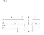
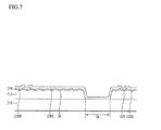
- Figs. 4 to 7 illustrate sectional views of the trans-reflective LCD shown in Fig. 3 during a manufacturing process of the trans-reflective LCD.
- the organic layer 215 is formed on the insulating substrate 210.
- the embossing 50 is formed in the surface of the organic layer 215 by photolithography.
- the reflection layer 218 is formed on the embossed organic layer 215 with a metal such as, but not limited to, Cr or Al.
- portions of the reflection layer 218, which are corresponding to transmission area TA, are removed, such as by a photo-etching process by using a photoresist layer 55 and a photo-mask 1000.
- the organic layer 215 is exposed through the removed portions of the reflection layer 218.
- the exposed portions of the organic layer 215 are removed to expose the insulating substrate 210.
- a step profile of the organic layer 215 is formed by simultaneous patterning of the organic layer 215 and the reflection layer 218. Accordingly, an LCD having multi cell gap is manufactured without using additional photo-etching process for forming the step profile of the organic layer 215. As a result, the manufacturing method of LCD having multi cell gap is simplified. Additionally, the LCD does not need an overcoating layer.
- the red, green, and blue color filters 230R, 230G, and 230B are formed on the light blocking layer.
- the color filters 230R, 230G, and 230B are disposed on both of the transmission area TA and the reflection area RA
- the common electrode 270 made of a transparent conductor such as Indium tin oxide (ITO) or Indium zinc oxide (IZO) is formed on the color filters 230R, 230G, and 230B and the light blocking layer 220
- the trans-reflection layer 218 is formed on the color filter panel that includes the color filters 230R, 230G, and 230B.
- the color filter panel is disposed as a lower panel and the thin film transistor array panel is disposed as an upper panel.
- This trans-reflective LCD structure allows manufacturing a trans-reflective LCD with using the same number of manufacturing steps with a transmission type LCD.
- the overcoating layer 250 formed on the trans-reflection layer 218 of the lower panel 200 has different thicknesses between the transmission area TA and the reflection area RA, a trans-reflective type LCD which has no phase difference between the transmission area TA and the reflection area RA without phase shifting films can advantageously be made. Production cost is lowered by omitting phase shifting films.
- the trans-reflective LCD according to an embodiment of the present invention shows an improved display quality.
- a step profile of the organic layer is formed by simultaneous patterning of the organic layer and the reflection layer. Accordingly, an LCD having multi cell gap is manufactured without using additional photo-etching process for forming the step profile of the organic layer As a result, the manufacturing method of LCD having multi cell gap is simplified. Additionally, the LCD of this embodiment advantageously does not require an overcoating layer.
- a stepped layer, whether an overcoating layer or an organic layer has a first thickness within the reflection area that is greater than a second thickness within the transmission area. In some embodiments, the second thickness may be zero.
Landscapes
- Physics & Mathematics (AREA)
- Nonlinear Science (AREA)
- Mathematical Physics (AREA)
- Chemical & Material Sciences (AREA)
- Crystallography & Structural Chemistry (AREA)
- General Physics & Mathematics (AREA)
- Optics & Photonics (AREA)
- Engineering & Computer Science (AREA)
- Microelectronics & Electronic Packaging (AREA)
- Liquid Crystal (AREA)
- Optical Filters (AREA)
Abstract
Description
Claims (25)
- A panel for an LCD device comprising:wherein a thickness of a portion of the overcoating layer corresponding to the reflection area is greater than that of a portion of the overcoating layer corresponding to the transmission area.a substrate;an organic layer formed on the substrate;a trans-reflection layer formed on the organic layer and having a reflection area reflecting a portion of incidence light from an exterior of the panel and a transmission area transmitting another portion of the incidence light;color filters formed on the trans-reflection layer;an overcoating layer formed on the color filters; anda common electrode formed on the overcoating layer,
- The panel for an LCD device of claim 1, wherein the overcoating layer is disposed at least on a portion of the trans-reflective layer corresponding to the reflection area.
- The panel for an LCD device of claim 1, further comprising an adhesion layer disposed between the overcoating layer and the common electrode.
- A panel for an LCD device comprising:wherein a thickness of a portion of the organic layer corresponding to the reflection area is greater than that of a portion of the organic layer corresponding to the transmission area.a substrate;an organic layer formed on the substrate;a trans-reflection layer formed on the organic layer and having a reflection area reflecting a portion of incidence light from an exterior of the panel and a transmission area transmitting another portion of the incidence light;color filters formed on the trans-reflection layer; anda common electrode formed on the color filters,
- The panel for an LCD device of claim 4, wherein the organic layer is disposed on the substrate at least within an area corresponding to the reflection area.
- The panel for an LCD device of any one of claims 1 or 4, wherein the trans-reflection layer is made of aluminum or chromium.
- The panel for an LCD device of any one of claims 1 or 4, wherein the organic layer has an embossed surface.
- The panel for an LCD device of any one of claims 1 or 4, wherein the color filters have light holes.
- A manufacturing method of a panel for an LCD device comprising:forming an organic layer on a substrate;embossing a surface of the organic layer;forming a reflection layer on the organic layer;removing a portion of the reflection layer to form a trans-reflection layer; andremoving a portion of the organic layer that is exposed through the portion of the reflection layer that is removed.
- The method of claim 9, wherein the portion of the reflection layer that is removed and the portion of the organic layer that is removed correspond to a transmission area.
- The method of claim 9, further comprising
forming color filters on the trans-reflection layer; and
forming a common electrode on the color filters. - The method of claim 9, wherein the removing a portion of the reflection layer to form a trans-reflection layer includes using a photo-etching process.
- An LCD device comprising:a first panel according to any one of claim 1 or claim 4;a second panel including a second substrate facing the first substrate; a plurality of thin film transistors formed on the second substrate; and a plurality of pixel electrodes connected to the thin film transistors, wherein the second panel is separated from the first panel by a selected gap; anda liquid crystal layer disposed between the first panel and the second panel.
- The LCD device of claim 13, wherein the overcoating layer is disposed at least on the portion of the trans-reflective layer corresponding to the reflection area.
- The LCD device of claim 13, wherein the organic layer is disposed on the first substrate at least within an area corresponding to the reflection area.
- The LCD device of claim 14 or claim 15, wherein the gap within the transmission area is larger than that within the reflection area.
- A panel for an LCD device comprising:a reflection area for reflecting within the panel a portion of incidence light from an exterior of the panel;a transmission area for transmitting through the panel another portion of the incidence light;a substrate; and,a stepped layer on the substrate, the stepped layer allowing the passage of the incidence light therethrough; wherein the stepped layer has a first thickness within the reflection area, and a second thickness within the transmission area, and wherein the first thickness is greater than the second thickness.
- The panel of claim 17, further comprising a trans-reflection layer including a reflection layer within the reflection area of the panel, the reflection layer reflecting the incidence light passing through the reflection area.
- The panel of claim 18, wherein the stepped layer is an organic layer formed on the substrate, and wherein the trans-reflection layer is formed on the organic layer.
- The panel of claim 19, wherein the organic layer includes an embossed surface for receiving the trans-reflection layer.
- The panel of claim 17, wherein the second thickness of the stepped layer is zero mm.
- The panel of claim 18, further comprising an organic layer disposed between the substrate and the trans-reflective layer, wherein the stepped layer is an overcoating layer formed upon a color filter layer on the trans-reflective layer.
- An LCD device comprising:wherein the gap has a first thickness within the reflection area and a second thickness within the transmission area, wherein the first thickness is less than the second thickness.a first panel;a second panel, the second panel separated from the first panel by a selected gap;a reflection area for reflecting within the first and second panels a portion of incidence light from an exterior of the first and second panels; and,a transmission area for transmitting through the first and second panels another portion of the incidence light;
- The LCD device of claim 23, wherein the first panel includes a common electrode and the second panel includes at least one thin film transistor and at least one pixel electrode connected to the thin film transistor.
- The LCD device of claim 23, further comprising a trans-reflection layer within the first panel, wherein the trans-reflection layer includes a reflection layer within the reflection area and a transmission layer within the transmission area.
Applications Claiming Priority (4)
| Application Number | Priority Date | Filing Date | Title |
|---|---|---|---|
| KR20040032643 | 2004-05-10 | ||
| KR2004032643 | 2004-05-10 | ||
| KR2004088309 | 2004-11-02 | ||
| KR1020040088309A KR20050107728A (en) | 2004-05-10 | 2004-11-02 | Lower display panel and liquid crystal display having the same |
Publications (2)
| Publication Number | Publication Date |
|---|---|
| EP1596244A2 true EP1596244A2 (en) | 2005-11-16 |
| EP1596244A3 EP1596244A3 (en) | 2006-03-29 |
Family
ID=34939769
Family Applications (1)
| Application Number | Title | Priority Date | Filing Date |
|---|---|---|---|
| EP05103891A Withdrawn EP1596244A3 (en) | 2004-05-10 | 2005-05-10 | Display panel and liquid crystal display device having the same |
Country Status (3)
| Country | Link |
|---|---|
| US (1) | US7830478B2 (en) |
| EP (1) | EP1596244A3 (en) |
| JP (1) | JP4712402B2 (en) |
Families Citing this family (4)
| Publication number | Priority date | Publication date | Assignee | Title |
|---|---|---|---|---|
| EP2261729B1 (en) | 2005-10-18 | 2014-05-07 | Semiconductor Energy Laboratory Co, Ltd. | Liquid crystal display device and electronic apparatus |
| KR20090050835A (en) * | 2007-11-16 | 2009-05-20 | 삼성전자주식회사 | Thin film transistor array panel and manufacturing method thereof |
| JP2010231178A (en) * | 2009-03-05 | 2010-10-14 | Seiko Epson Corp | Electro-optical device substrate, electro-optical device, and electronic apparatus |
| KR20150083684A (en) | 2014-01-10 | 2015-07-20 | 삼성디스플레이 주식회사 | Display device and fabrication method thereof |
Citations (2)
| Publication number | Priority date | Publication date | Assignee | Title |
|---|---|---|---|---|
| JP2004271723A (en) * | 2003-03-06 | 2004-09-30 | Seiko Epson Corp | Display device and electronic equipment |
| US20040201804A1 (en) * | 2003-04-09 | 2004-10-14 | Toppoly Optoelectronics Corp. | Transflective liquid crystal display device |
Family Cites Families (15)
| Publication number | Priority date | Publication date | Assignee | Title |
|---|---|---|---|---|
| JP2000098371A (en) | 1998-09-17 | 2000-04-07 | Omron Corp | Reflective image display device and display device substrate |
| JP3649075B2 (en) | 2000-02-29 | 2005-05-18 | 株式会社日立製作所 | Liquid crystal display |
| US6812978B2 (en) * | 2000-02-29 | 2004-11-02 | Lg.Philips Lcd Co., Ltd. | Method for fabricating transflective color LCD device and the transflective color LCD device with thick and thin regions of color filter layer |
| JP2002162645A (en) * | 2000-09-14 | 2002-06-07 | Sony Corp | Transflective liquid crystal display |
| JP2002311424A (en) * | 2001-04-12 | 2002-10-23 | Hitachi Ltd | Liquid crystal display |
| JP3675427B2 (en) | 2001-09-25 | 2005-07-27 | セイコーエプソン株式会社 | Transflective liquid crystal device and electronic equipment using the same |
| JP4302385B2 (en) * | 2001-10-22 | 2009-07-22 | 三星電子株式会社 | Liquid crystal display device for improving reflectivity and manufacturing method thereof |
| KR100858295B1 (en) * | 2002-02-26 | 2008-09-11 | 삼성전자주식회사 | Reflective-transmissive liquid crystal display and manufacturing method thereof |
| KR100790357B1 (en) * | 2002-02-26 | 2008-01-02 | 엘지.필립스 엘시디 주식회사 | Color filter substrate for reflective transmissive liquid crystal display and manufacturing method |
| JP4082106B2 (en) | 2002-06-26 | 2008-04-30 | 凸版印刷株式会社 | Color filter for transflective LCD and method for manufacturing the same |
| TWI259923B (en) * | 2002-08-01 | 2006-08-11 | Boe Hyids Technology Co Ltd | Liquid crystal display |
| JP4182748B2 (en) * | 2002-12-20 | 2008-11-19 | セイコーエプソン株式会社 | Liquid crystal display device and electronic device |
| JP4181905B2 (en) * | 2003-03-25 | 2008-11-19 | アルプス電気株式会社 | Liquid crystal display panel and liquid crystal display device |
| KR101012494B1 (en) * | 2003-04-04 | 2011-02-08 | 엘지디스플레이 주식회사 | Reflective type liquid crystal display device |
| JP4317705B2 (en) * | 2003-04-24 | 2009-08-19 | シャープ株式会社 | Liquid crystal display |
-
2005
- 2005-01-28 JP JP2005021057A patent/JP4712402B2/en not_active Expired - Lifetime
- 2005-05-10 EP EP05103891A patent/EP1596244A3/en not_active Withdrawn
- 2005-05-10 US US11/125,669 patent/US7830478B2/en active Active
Patent Citations (2)
| Publication number | Priority date | Publication date | Assignee | Title |
|---|---|---|---|---|
| JP2004271723A (en) * | 2003-03-06 | 2004-09-30 | Seiko Epson Corp | Display device and electronic equipment |
| US20040201804A1 (en) * | 2003-04-09 | 2004-10-14 | Toppoly Optoelectronics Corp. | Transflective liquid crystal display device |
Also Published As
| Publication number | Publication date |
|---|---|
| US7830478B2 (en) | 2010-11-09 |
| JP4712402B2 (en) | 2011-06-29 |
| EP1596244A3 (en) | 2006-03-29 |
| US20050248703A1 (en) | 2005-11-10 |
| JP2005321756A (en) | 2005-11-17 |
Similar Documents
| Publication | Publication Date | Title |
|---|---|---|
| US8035779B2 (en) | Thin film transistor display panel, liquid crystal display having the same, and method of manufacturing liquid crystal display | |
| US6879359B1 (en) | Reflection type liquid crystal display provided with reflective layer, coplanar gate electrode, color filter layer and transparent pixel electrode and manufacture method thereof | |
| US7977679B2 (en) | Thin film transistor array panel | |
| US8274616B2 (en) | Array substrate for liquid crystal display device and method of manufacturing the same | |
| US8842248B2 (en) | Display device | |
| US8896790B2 (en) | Liquid crystal display with opposing protrusions in a pixel | |
| KR20100020140A (en) | Thin film transistor display panel and method of manufacturing of the same | |
| KR101293561B1 (en) | Thin film transistor panel and manufacturing method thereof | |
| US20060131581A1 (en) | Thin film transistor array panel and method for manufacturing the same | |
| US8085366B2 (en) | Thin film transistor display panel and method of manufacturing the same | |
| JP2006301089A (en) | Liquid crystal display and its manufacturing method | |
| US8017947B2 (en) | Thin film transistor array panel, display device including the same, and method thereof | |
| US20070126958A1 (en) | Liquid crystal display and panel therefor | |
| US20050264722A1 (en) | Liquid crystal display and manufacturing method thereof | |
| US7876402B2 (en) | Liquid crystal display device | |
| US7847889B2 (en) | Panel for display device with light blocking on blue color filter and liquid crystal display | |
| US20060157705A1 (en) | Thin film transistor array panel | |
| CN100517034C (en) | Display device and thin film transistor array panel and manufacturing method thereof | |
| US20040257500A1 (en) | Liquid crystal display | |
| US7714964B2 (en) | Transflective liquid crystal display | |
| US20040114071A1 (en) | Color filter panel, manufacturing method thereof and transflective liquid crystal display including the same | |
| US7830478B2 (en) | Display panel and liquid crystal display device having the same | |
| CN1702535B (en) | Display panel and liquid crystal display device having the display panel | |
| US8685770B2 (en) | Thin film transistor array panel and method for manufacturing the same | |
| KR20060017964A (en) | Transflective type liquid crystal display device and transflective type liquid crystal display device |
Legal Events
| Date | Code | Title | Description |
|---|---|---|---|
| PUAI | Public reference made under article 153(3) epc to a published international application that has entered the european phase |
Free format text: ORIGINAL CODE: 0009012 |
|
| AK | Designated contracting states |
Kind code of ref document: A2 Designated state(s): AT BE BG CH CY CZ DE DK EE ES FI FR GB GR HU IE IS IT LI LT LU MC NL PL PT RO SE SI SK TR |
|
| AX | Request for extension of the european patent |
Extension state: AL BA HR LV MK YU |
|
| RIN1 | Information on inventor provided before grant (corrected) |
Inventor name: PARK, SANG-WOO Inventor name: JEON, YONG-JE Inventor name: KIM, BONG-JU Inventor name: HIRAI, AKIRA Inventor name: LEE, HO-JUNG Inventor name: LEE, EUNG-SANG |
|
| PUAL | Search report despatched |
Free format text: ORIGINAL CODE: 0009013 |
|
| AK | Designated contracting states |
Kind code of ref document: A3 Designated state(s): AT BE BG CH CY CZ DE DK EE ES FI FR GB GR HU IE IS IT LI LT LU MC NL PL PT RO SE SI SK TR |
|
| AX | Request for extension of the european patent |
Extension state: AL BA HR LV MK YU |
|
| 17P | Request for examination filed |
Effective date: 20060601 |
|
| AKX | Designation fees paid |
Designated state(s): FR IT |
|
| REG | Reference to a national code |
Ref country code: DE Ref legal event code: 8566 |
|
| 17Q | First examination report despatched |
Effective date: 20110221 |
|
| RAP1 | Party data changed (applicant data changed or rights of an application transferred) |
Owner name: SAMSUNG ELECTRONICS CO., LTD. |
|
| RAP1 | Party data changed (applicant data changed or rights of an application transferred) |
Owner name: SAMSUNG DISPLAY CO., LTD. |
|
| RAP1 | Party data changed (applicant data changed or rights of an application transferred) |
Owner name: SAMSUNG DISPLAY CO., LTD. |
|
| STAA | Information on the status of an ep patent application or granted ep patent |
Free format text: STATUS: THE APPLICATION IS DEEMED TO BE WITHDRAWN |
|
| 18D | Application deemed to be withdrawn |
Effective date: 20190409 |