EP1591826A1 - Spread illuminating apparatus - Google Patents
Spread illuminating apparatus Download PDFInfo
- Publication number
- EP1591826A1 EP1591826A1 EP05005456A EP05005456A EP1591826A1 EP 1591826 A1 EP1591826 A1 EP 1591826A1 EP 05005456 A EP05005456 A EP 05005456A EP 05005456 A EP05005456 A EP 05005456A EP 1591826 A1 EP1591826 A1 EP 1591826A1
- Authority
- EP
- European Patent Office
- Prior art keywords
- prisms
- conductive plate
- light
- light conductive
- illuminating apparatus
- Prior art date
- Legal status (The legal status is an assumption and is not a legal conclusion. Google has not performed a legal analysis and makes no representation as to the accuracy of the status listed.)
- Granted
Links
- 230000003746 surface roughness Effects 0.000 claims description 5
- 238000009826 distribution Methods 0.000 description 24
- 238000012986 modification Methods 0.000 description 12
- 230000004048 modification Effects 0.000 description 12
- 238000005520 cutting process Methods 0.000 description 10
- 238000003754 machining Methods 0.000 description 10
- 229920005989 resin Polymers 0.000 description 10
- 239000011347 resin Substances 0.000 description 10
- 238000012360 testing method Methods 0.000 description 8
- 239000004973 liquid crystal related substance Substances 0.000 description 7
- 238000000465 moulding Methods 0.000 description 7
- 230000001788 irregular Effects 0.000 description 6
- 239000000463 material Substances 0.000 description 6
- CERQOIWHTDAKMF-UHFFFAOYSA-M Methacrylate Chemical compound CC(=C)C([O-])=O CERQOIWHTDAKMF-UHFFFAOYSA-M 0.000 description 4
- 230000000052 comparative effect Effects 0.000 description 4
- 229920005668 polycarbonate resin Polymers 0.000 description 4
- 239000004431 polycarbonate resin Substances 0.000 description 4
- 238000009792 diffusion process Methods 0.000 description 3
- 230000000694 effects Effects 0.000 description 3
- 229920002799 BoPET Polymers 0.000 description 2
- 230000003247 decreasing effect Effects 0.000 description 2
- 229920005672 polyolefin resin Polymers 0.000 description 2
- 230000005540 biological transmission Effects 0.000 description 1
- 230000001413 cellular effect Effects 0.000 description 1
- 230000007547 defect Effects 0.000 description 1
- 230000000593 degrading effect Effects 0.000 description 1
- 230000003292 diminished effect Effects 0.000 description 1
- 230000002708 enhancing effect Effects 0.000 description 1
- 239000003822 epoxy resin Substances 0.000 description 1
- NBVXSUQYWXRMNV-UHFFFAOYSA-N fluoromethane Chemical compound FC NBVXSUQYWXRMNV-UHFFFAOYSA-N 0.000 description 1
- 238000001746 injection moulding Methods 0.000 description 1
- 238000005304 joining Methods 0.000 description 1
- 238000004519 manufacturing process Methods 0.000 description 1
- 230000003287 optical effect Effects 0.000 description 1
- 229920000647 polyepoxide Polymers 0.000 description 1
- 229920001225 polyester resin Polymers 0.000 description 1
- 239000004645 polyester resin Substances 0.000 description 1
- 229920005990 polystyrene resin Polymers 0.000 description 1
Images





Classifications
-
- G—PHYSICS
- G02—OPTICS
- G02B—OPTICAL ELEMENTS, SYSTEMS OR APPARATUS
- G02B6/00—Light guides; Structural details of arrangements comprising light guides and other optical elements, e.g. couplings
- G02B6/0001—Light guides; Structural details of arrangements comprising light guides and other optical elements, e.g. couplings specially adapted for lighting devices or systems
- G02B6/0011—Light guides; Structural details of arrangements comprising light guides and other optical elements, e.g. couplings specially adapted for lighting devices or systems the light guides being planar or of plate-like form
- G02B6/0033—Means for improving the coupling-out of light from the light guide
- G02B6/005—Means for improving the coupling-out of light from the light guide provided by one optical element, or plurality thereof, placed on the light output side of the light guide
- G02B6/0053—Prismatic sheet or layer; Brightness enhancement element, sheet or layer
-
- G—PHYSICS
- G02—OPTICS
- G02B—OPTICAL ELEMENTS, SYSTEMS OR APPARATUS
- G02B6/00—Light guides; Structural details of arrangements comprising light guides and other optical elements, e.g. couplings
- G02B6/0001—Light guides; Structural details of arrangements comprising light guides and other optical elements, e.g. couplings specially adapted for lighting devices or systems
- G02B6/0011—Light guides; Structural details of arrangements comprising light guides and other optical elements, e.g. couplings specially adapted for lighting devices or systems the light guides being planar or of plate-like form
- G02B6/0033—Means for improving the coupling-out of light from the light guide
- G02B6/0035—Means for improving the coupling-out of light from the light guide provided on the surface of the light guide or in the bulk of it
- G02B6/0038—Linear indentations or grooves, e.g. arc-shaped grooves or meandering grooves, extending over the full length or width of the light guide
-
- G—PHYSICS
- G02—OPTICS
- G02F—OPTICAL DEVICES OR ARRANGEMENTS FOR THE CONTROL OF LIGHT BY MODIFICATION OF THE OPTICAL PROPERTIES OF THE MEDIA OF THE ELEMENTS INVOLVED THEREIN; NON-LINEAR OPTICS; FREQUENCY-CHANGING OF LIGHT; OPTICAL LOGIC ELEMENTS; OPTICAL ANALOGUE/DIGITAL CONVERTERS
- G02F1/00—Devices or arrangements for the control of the intensity, colour, phase, polarisation or direction of light arriving from an independent light source, e.g. switching, gating or modulating; Non-linear optics
- G02F1/01—Devices or arrangements for the control of the intensity, colour, phase, polarisation or direction of light arriving from an independent light source, e.g. switching, gating or modulating; Non-linear optics for the control of the intensity, phase, polarisation or colour
- G02F1/13—Devices or arrangements for the control of the intensity, colour, phase, polarisation or direction of light arriving from an independent light source, e.g. switching, gating or modulating; Non-linear optics for the control of the intensity, phase, polarisation or colour based on liquid crystals, e.g. single liquid crystal display cells
- G02F1/133—Constructional arrangements; Operation of liquid crystal cells; Circuit arrangements
- G02F1/1333—Constructional arrangements; Manufacturing methods
- G02F1/1335—Structural association of cells with optical devices, e.g. polarisers or reflectors
- G02F1/1336—Illuminating devices
- G02F1/133615—Edge-illuminating devices, i.e. illuminating from the side
Definitions
- the present invention relates to a spread illuminating apparatus as a lighting means for a liquid crystal display apparatus, and more specifically to a side light type illuminating apparatus using a point light source.
- LCD liquid crystal display
- a transmission type LCD apparatus requires a lighting means for illuminating its liquid crystal panel, and also a semi-transmission type LCD apparatus which utilizes outside light must have an auxiliary lighting means for enabling a usage in the dark.
- a side light type illuminating apparatus mainly comprises a light conductive plate and a light source disposed at a side surface of the light conductive plate, readily enables its profile to be lowered, and therefore can be suitably used as a lighting means for the LCD apparatus, for which a cold cathode tube, that is a line light source, is conventionally used.
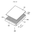
- Fig. 12 is an exploded perspective view of a conventional side light type spread illuminating apparatus 100 having such a light converging means as described above.
- the spread illuminating apparatus 100 comprises a light conductive plate 101 defining a light entrance surface 101c, a light reflection surface 101b and a light exit surface 101a, a line light source 102 disposed at the light entrance surface 101c of the light conductive plate 101, and a prism sheet 103 disposed on the light exit surface 101a of the light conductive plate 101.
- the light conductive plate 101 is formed of a transparent resin material, such as methacrylate resin, polycarbonate resin, and the like.
- a plurality of triangular prisms are formed which are shaped identical with one another, extend in a direction orthogonal to the light entrance surface 101c, and which are arrayed at a regular interval.
- a diffuse or regular reflecting means (not shown) is provided which reflects light toward the light exit surface 101a so that the light impinges on the light exit surface 101a at an angle less than an critical angle.
- the prism sheet 103 is formed of a transparent resin material, for example a PET film, and has, on a major surface (prism surface) 103a thereof, a plurality of triangular prisms which are formed of a transparent resin material, such as methacrylate resin, polycarbonate resin, and the like, and which extend in one same direction.
- the prism sheet 103 is disposed on the light conductive plate 101 such that the prism surface 103a faces the light exit surface 101a with their respective triangular prisms extending orthogonally to each other.
- a direction orthogonal to the light entrance surface 101c of the light conductive plate 101 is defined as an X-axis direction
- a direction normal to the light exit surface 101a of the light conductive plate 101 is defined as a Z-axis direction
- a direction perpendicular to both the X-axis and Z-axis directions is defined as a Y-axis direction.
- planes defined by the coordinate axes (X, Y, Z) shown in Fig. 12 are referred to as an XY plane, a YZ plane, and an XZ plane, which will be used also for any planes parallel thereto.
- light emitted from the line light source 102 is introduced into the light conductive plate 101 through the light entrance surface 101c thereof, then partly exits out from the light exit surface 101a while traveling inside the light conductive plate 101 with repeated reflections at the light reflection surface 101b and the light exit surface 101a, and finally illuminates a liquid crystal panel, or the like as an object illuminated.
- the YZ plane directivity of the light is compensated with respect to the XZ plane by means of the triangular prisms formed on the light exit surface 101a, and then the XZ plane directivity of the light is compensated with respect to the YZ plane by means of the triangular prisms formed on the prism surface 103a of the prism sheet 103, whereby brightness for the Z-axis direction neighborhood, which is the front brightness, is enhanced.
- This arrangement is advantageous compared with an arrangement in which two prism sheets are disposed on a light exit surface of a light conductive plate with their respective prisms extending orthogonally to each other such that their respective plain surfaces opposite to the prism surfaces face toward the light exit surface of the light conductive plate, in that the number of expensive prism sheets is reduced, and in that light exiting out the light conductive plate is not reflected at the plane surfaces of the prism sheets so as to go back to the light conductive plate.
- the light reflection surface 101b is provided with a regular reflecting means comprising, for example, V-shaped grooves extending in the Y-axis direction so that light reflected by such a reflecting means falls incident on the light exit surface 101a at an angle slightly smaller than a critical angle, then the light exits out from the light exit surface 101a with a narrow directivity inclined in the X-axis direction within the ZX plane, whereby the light converging efficiency is improved resulting in further enhanced brightness.
- a white light emitting diode (LED) with enhanced performance is increasingly used as a point light source in a spread illuminating apparatus for the purpose of downsizing and lowering power consumption.
- a line light source emits light with comparatively uniform brightness along its length direction
- a plurality of point light sources which are disposed in a line and parallel to a light entrance surface of a light conductive plate, have respective different brightness distributions with their peaks positioned at the front direction, which causes light outgoing from the apparatus to involve brightness variation unless a uniformizing means is provided.
- a uniformizing means is provided.
- the present inventor proposed previously in Japanese Patent Application No. 2002-368805 a spread illuminating apparatus which incorporates a light diffusing means.
- the light diffusing means disclosed therein comprises a plurality of prisms of various kinds extending in the direction orthogonal to a light entrance surface of a light conductive plate.
- the prisms include circular arcs in cross-section taken along a line perpendicular to the extension direction, and the maximum tangential angles of respective circular arcs with respect to a principal virtual plane are different from one another.
- the prisms which constitute the light diffusing means of the light conductive plate in the spread illuminating apparatus disclosed in the aforementioned Japanese Patent Application No. 2002-368805, may have their respective heights differing from one another, and therefore a prism sheet to be disposed on the light conductive plate is supported only partly by some of the prisms of the light diffusing means that have relatively large heights, rather than entirely by all of the prisms. Consequently, when the illuminating apparatus is subjected to vibration or change of ambient temperature, the contact portions of both the light conductive plate and the prism sheet may have scratches, and the scratches are viewed as emission lines (defects) thus degrading the display quality on the object illuminated.
- the present invention has been made in light of the above problem, and it is an object of the present invention to provide a side light type spread illuminating apparatus with a light conductive plate which incorporates a light diffusing means while preventing scratches.
- a spread illuminating apparatus comprising: a light conductive plate having a light exit surface provided with a plurality of prisms which define one extension direction; at least one point light source disposed at a side surface of the light conductive plate; and a prism sheet which has a prism surface provided with a plurality of prisms defining one extension direction, and which is disposed on the light conductive plate such that the prism surface faces the light exit surface of the light conductive plate, and that the extension direction of the prisms of the prism sheet is oriented substantially orthogonal to the extension direction of the prisms of the light conductive plate, the plurality of prisms of the light conductive plate have respective configurations different from one another in cross section taken along a line orthogonal to the extension direction, and respective ridges of the plurality of prisms are located on a common virtual plane.
- the prisms of the light conductive plate have the same height, and therefore the prisms of the prism sheet disposed on the light conductive plate are supported evenly by all of the prisms of the light conductive plate, which results in that the load of the prism sheet gives reduced pressure to each of the prisms, and also that the prism sheet sits stably on the light conductive plate, whereby the light conductive plate is better prevented from getting scratched.
- the extension direction of the prisms of the light conductive plate may be substantially orthogonal to the side surface of the light conductive plate, at which the at least one point light source is disposed. Consequently, light exiting out from the light exit surface of the light conductive plate is diffused in the direction parallel to the side surface of the light conductive plate thereby reducing the non-uniformity of brightness distribution of the light.
- the prisms of the light conductive plate may be arrayed such that distances each defined between apexes of adjacent two of the prisms differ irregularly from one another. Consequently, the non-uniformity of the light brightness distribution is further reduced, and Moire fringes resulting from interference with the pixel period of a liquid crystal panel can be better prevented from occurring.
- the prisms of the light conductive plate may have respective circular arc configurations with a common curvature in cross section taken the line orthogonal to the extension direction thereof, and two tangential angles at respective butting ends of adjacent two of the prisms of the light conductive plate may be equal to each other. Consequently, a molding die for forming the light conductive plate can be produced by using only one kind cutting tool and setting the cutting depth, only requiring control of transfer distance. This contributes to decreasing the cost of the molding die.
- overall tangential angles at respective ends of the prisms of the light conductive plate may be arranged to vary irregularly within a range of 40 to 70 degrees.
- the prisms of the light conductive plate may have respective circular arc configurations with a common curvature in cross section taken the line orthogonal to the extension direction thereof, and the prisms of the light conductive plate may be arrayed such that distances each defined between apexes of adjacent two of the prisms of the light conductive plate differ irregularly from one another within a range of 10 to 200 ⁇ m.
- the prisms of the light conductive plate may have their surfaces roughened with micro ridges and grooves extending in one direction parallel to the extension direction of the prisms of the light conductive plate. Consequently, the non-uniformity of the light brightness distribution can be markedly reduced.
- the roughened surfaces of the prisms of the light conductive plate may have an average surface roughness of 0.1 to 1.0 ⁇ m.
- a spread illuminating apparatus 10 comprises a light conductive plate 11, a plurality (three in the figure) of point light sources 12, and a prism sheet 13.
- the point light sources 12 are white LED's
- the light conductive plate 11 is formed of a transparent resin material, such as methacrylate resin, polycarbonate resin, polystyrene resin, polyolefin resin, amorphous polyolefin resin, polyester resin, transparent fluorocarbon resin, and epoxy resin.
- the prism sheet 13 is composed of, for example, a PET film based material, and defines a prism surface 13a provided with a plurality of prisms which are formed of methacrylate resin, polycarbonate resin, or the like, have a triangular cross section, and which extend in one same direction.
- the point light sources 12 are disposed parallel to a light entrance surface 11c of the light conductive plate 11, and the prism sheet 13 is placed on one major surface (light exit surface) 11a of the light conductive plate 11 with the prism surface 13a facing the light exit surface 11a.
- the light exit surface 11a of the light conductive plate 11 is provided with a plurality of prisms extending in the direction orthogonal to the light entrance surface 11c, and the prism sheet 13 is disposed with the extension direction of its prisms oriented perpendicular to the extension direction of the plurality of prisms formed at the light exit surface 11a of the light conductive plate 11.
- the prisms at the light exit surface 11a are schematically illustrated as a group of straight lines in Fig. 1 and will be detailed later.
- the other major surface (light reflection surface) 11b of the light conductive plate 11 is provided with a regular reflecting means comprising a plurality of prisms, which are each composed of inclined surfaces 14a and 14b, extend in the direction parallel to the light entrance surface 11c, and which are arrayed in the direction orthogonal to the light entrance surface 11c.
- the areas and inclination angles of the inclined surfaces 14a and 14b and the intervals of the prism array are appropriately determined in consideration of the uniformity of brightness distribution depending on the distance from the light entrance surface 11c.
- the light conductive plate 11 does not have to use the regular reflecting means as shown in Fig. 1 but may alternatively use a diffuse reflecting means with a dot pattern composed of a plurality of dots.
- the light conductive plate 11 in Fig. 1 is shaped into wedge configuration with its thickness decreasing from the light entrance surface 11c toward the other surface opposite thereto, but may alternatively be a simple plate with a constant thickness all the way.
- a plane defined as a reference surface for the prisms is referred to as a "principal virtual plane" of a light conductive plate.
- a direction orthogonal to the light entrance surface 11c is referred to as an X-axis direction
- a direction normal to the principal virtual plane is referred to as a Z-axis direction
- a direction orthogonal to both the X-axis and Z-axis directions is referred to as a Y-axis direction.
- XY plane 1 are referred to as an XY plane, a YZ plane, and an XZ plane, which will also apply to any planes oriented parallel thereto.
- the peak point of each prism in the Z-axis direction is referred to as an "apex”, and a straight line formed by continuously connecting the apexes in the X-axis direction is referred to as a "ridge”.
- Fig. 2A is a cross-sectional view (partly omitted) of the light conductive plate 11 taken along a line parallel to the light entrance surface 11c (the section is referred to as YZ section), and Fig. 2B is an enlarged view of a portion of the cross section shown in Fig. 2A.
- a plurality of circular prisms C 1 to C N are formed so as to have a circular arc with an identical curvature in the YZ section.
- Apexes of the circular prisms C 1 to C N are aligned to a virtual straight line shown by a dashed line m, and any virtual straight line shifted in the X-axis direction is included in one virtual plane.
- the circular prisms C 1 to C N are formed with their respective ridges located on a common virtual plane. Accordingly, in the spread illuminating apparatus 10, the prism sheet 13 is disposed on the light exit surface 11a of the light conductive plate 11 in such a manner that each of the prisms of the prism sheet 13 extending in the Y-axis direction is supported entirely by all of the circular prisms C 1 to C N .
- the virtual plane on which the ridges of the circular prisms C 1 to C N are located, is oriented parallel to the principal plane which is a reference plane for the height of each of the circular prisms C 1 to C N , that is to say, the circular prisms C 1 to C N define respective cylindrical surfaces, and all have one same height (dimension in the Z-axis direction) that keeps constant in the X-axis direction, but the present invention is not limited thereto and the virtual plane does not have to be oriented parallel to the principal virtual plane.
- Respective distances between the apexes of adjacent two of the circular prisms C 1 to C N are defined as distances Wi to W N-1 between the ridges thereof, and are irregularly arranged.
- Each distance W k ( 1 ⁇ k ⁇ N-1 ) is appropriately set in consideration of brightness distribution uniformity, and workability in die machining to be described later, preferably to fall between 10 and 200 ⁇ m. Also, referring to Fig.
- the plurality of circular prisms which define respective tangential angles different from one another, and each of which has two different tangential angles ⁇ k and ⁇ k ( ⁇ 1 and ⁇ N are tangential angles at the extreme ends of the circular prisms arrayed) at its both circular arc ends, are arrayed at irregular intervals on the light exit surface 11a of the light conductive plate 11.
- Each of the tangential angles ⁇ k and ⁇ k (1 ⁇ k ⁇ N ) is appropriately set in consideration of brightness distribution uniformity, and workability in die machining to be described later, preferably to fall between 40 and 70 degrees.
- light emitted from each of the point light sources 12 is introduced into the light conductive plate 11 from the light entrance surface 11c, reflected at the light exit surface 11a and the light reflection surface 11b while traveling in the light conductive plate 11, exits out light conductive plate 11 when impinging on the light exit surface 11a at an angle smaller than a critical angle, and illuminates an object, for example, an LCD apparatus.
- the emission direction of the light in the XZ plane is corrected with respect to the YZ plane by means of the prisms of the prism sheet 13 extending in the Y-axis direction, thereby increasing the brightness in the Z-axis direction neighbor, that is, front brightness.
- the circular prisms C 1 to C N are arrayed at irregular intervals on the light exit surface 11a of the light conductive plate 11 with respect to the Y-axis direction so that the surfaces of the circular prisms C 1 to C N make various inclinations relative to the principal virtual plane, the emission direction of the light exiting out from the light exit surface 11a of the light conductive plate 11 is diffused effectively in the Y-axis direction, thereby reducing the non-uniformity of brightness distribution in the Y-axis direction. Also, since the ridges of the circular prisms C 1 to C N are located at a common virtual plane, the prism sheet 13 is supported evenly by all of the circular prisms C 1 to C N so as to stably sit on the light conductive plate 11.
- a light conductive plate 21 shown in the YZ section has a plurality of circular prisms divided into a plurality of units L repeatedly arrayed, each of which is composed of a plurality (three in the figure) of different circular prisms C 1 , C 2 and C 3 defining different distances W 1 and W 2 between their respective apexes.
- a dimension between the apexes of two abutting prisms of two adjacent units L is defined as a distance d, and respective distances d may be equal to one another or may alternatively differ from one another in a regular or irregular manner.
- the number of circular prisms constituting the unit L, and the distance between the apexes of the prisms are appropriately set in consideration of brightness distribution uniformity, and workability in die machining to be described later.
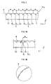
- a light conductive plate 31 has, at its light emit surface, a plurality of circular prisms C k ( 1 ⁇ k ⁇ N ) which have an identical cross section with one another, and each of which has its surface roughened by various micro ridges and grooves extending in the X-axis direction (refer to Fig. 4B).
- each prism surface has a plurality of micro prisms different from one another so that micro surfaces differently inclined relative to the principal virtual plane are irregularly arrayed in the Y-axis direction, whereby the emission direction of the light exiting out from the light exit surface of the light conductive plate 31 is diffused effectively in the Y-axis direction so as to reduce the non-uniformity of brightness distribution in the Y-axis direction.
- the average surface roughness is preferably set to range from 0.1 to 1.0 ⁇ m in terms of a center line average roughness Ra defined by JIS B 0601-1982.
- the distance W k and the tangential angles ( ⁇ k , ⁇ k ) about the circular prism C k are appropriately set in consideration of brightness distribution uniformity, and workability in die machining to be described later.
- This structure of roughened prism surfaces may be preferably combined with the light conductive plates 11 and 21 shown in Figs.2A and 2B, and Fig. 3, respectively, which will demonstrate an outstanding diffusion effect.
- a second embodiment of the present invention will be described with reference to Figs. 5A to 7B.
- a spread illuminating apparatus according to the second embodiment includes the same components as illustrated in Fig. 1 except a light conductive plate, and therefore an illustration thereof is omitted.
- any component parts corresponding to those in Fig. 1 are denoted by the same reference numerals except the light conductive plate and its relevant portions.
- Fig. 5A is a cross-sectional view (partly omitted) of a light conductive plate 41 taken along a line parallel to a light entrance surface 41c thereof (YZ section), and Fig. 5B is an enlarged view of a portion of the cross section shown in Fig. 5A.
- the light conductive plate 41 has, at a light exit surface 41a thereof, a plurality of triangular prisms T 1 to T N ( N is a predetermined positive integer) which have a isosceles triangular shape with respective different apex angles ⁇ 1 to ⁇ N in the YZ section, and which extend in the X-axis direction and are arrayed in a random sequence with respect to the Y-axis direction.
- Apexes of the triangular prisms T 1 to T N are aligned to a virtual straight line shown by a dashed line m, and any virtual straight line shifted in the X-axis direction is included in one virtual plane.
- the triangular prisms T 1 to T N are formed with their respective ridges located on a common virtual plane. Accordingly, in the spread illuminating apparatus 10, the prism sheet 13 is disposed on the light exit surface 41a of the light conductive plate 41 in such a manner that each of the prisms of the prism sheet 13 extending in the Y-axis direction is supported by all of the triangular prisms T 1 to T N .
- the virtual plane, on which the ridges of the triangular prisms T 1 to T N are located is oriented parallel to the principal plane which is a reference plane for the height of each of the triangular prisms T 1 to T N , that is to say, the triangular prisms T 1 to T N constitute respective triangular column, and all have one same height (dimension in the Z-axis direction) that keeps constant in the X-axis direction, but the present invention is not limited thereto and the virtual plane does not have to be oriented parallel to the principal virtual plane.
- Respective distances between the apexes of adjacent two of the triangular prisms T 1 to T N are defined as distances W 1 to W N-1 between the ridges thereof, and are irregularly arranged.
- Each distance W k ( 1 ⁇ k ⁇ N-1 ) is appropriately set in consideration of brightness distribution uniformity, and workability in die machining to be described later, preferably to fall between 10 and 200 ⁇ m.
- the apex angle ⁇ k ( 1 ⁇ k ⁇ N ) ranges from 50 to 160 degrees, preferably from 130 to 160 degrees.
- the triangular prisms T 1 to T N are formed to have an isosceles triangular cross section in the embodiment described above but do not have to be formed so, and may alternatively be formed in a triangle with its two inclined sides making respective different angles ⁇ k and ⁇ k with respect to the principal virtual plane.
- light emitted from each of the point light sources 12 is introduced into the light conductive plate 41 from the light entrance surface 41c, reflected at the light exit surface 41a and the light reflection surface 41b while traveling in the light conductive plate 41, exits out light conductive plate 41 when impinging on the light exit surface 41a at an angle smaller than a critical angle, and illuminates an object, for example, an LCD apparatus.
- the emission direction of the light in the XZ plane is corrected with respect to the YZ plane by means of the prisms of the prism sheet 13 extending in the Y-axis direction, thereby increasing the brightness in the Z-axis direction neighbor, that is, front brightness.
- the triangular prisms T 1 to T N which are shaped in isosceles triangle with respective different apex angles, are arrayed on the light exit surface 41a of the light conductive plate 41 in a random sequence with respect to the Y-axis direction so that a plurality of micro inclined surfaces with various inclinations relative to the principal virtual plane are provided irregularly in the Y-axis direction, the emission direction of the light exiting out from the light exit surface 41a of the light conductive plate 41 is diffused effectively in the Y-axis direction, thereby reducing the non-uniformity of brightness distribution in the Y-axis direction.
- the prism sheet 13 is supported evenly by all the triangular prisms T 1 to T N so as to stably sit on the light conductive plate 41.
- a light conductive plate 51 shown in the YZ section has a plurality of triangular prisms divided into a plurality of units L repeatedly arrayed, each of which is composed of a plurality (three in the figure) of different triangular prisms T 1 , T 2 and T 3 defining different distances W 1 and W 2 between their respective apexes.
- a dimension between the apexes of two abutting prisms of two adjacent units L is defined as a distance d, and respective distances d may be equal to one another or may alternatively differ from one another in a regular or irregular manner.
- the number of triangular prisms constituting the unit L, and the distance between the apexes of the prisms are appropriately set in consideration of brightness distribution uniformity, and workability in die machining to be described later.
- a light conductive plate 61 has, at its light emit surface, a plurality of triangular prisms T k ( 1 ⁇ k ⁇ N ) which have an identical cross section with one another, and each of which has its inclined surfaces roughened by various micro ridges and grooves extending in the X-axis direction (refer to Fig. 7B).
- each prism surface has a plurality of micro prisms different from one another so that micro surfaces differently inclined relative to the principal virtual plane are irregularly arrayed in the Y-axis direction, whereby the emission direction of the light exiting out from the light exit surface of the light conductive plate 61 is diffused effectively in the Y-axis direction so as to reduce the non-uniformity of brightness distribution in the Y-axis direction.
- the average surface roughness is preferably set to range from 0.1 to 1.0 ⁇ m in terms of a center line average roughness Ra defined by JIS B 0601-1982.
- the distance W k and the tangential angles ( ⁇ k , ⁇ k , ⁇ k ) about the triangular prism T k are appropriately set in consideration of brightness distribution uniformity, and workability in die machining to be described later.
- This structure of roughened prism surfaces may be preferably combined with the light conductive plates 41 and 51 shown in Figs.5A and 5B, and Fig. 6, respectively, which will demonstrate an outstanding diffusion effect.
- a third embodiment of the present invention will be described with reference to Figs. 8A to 10B.
- a spread illuminating apparatus according to the third embodiment includes the same components as illustrated in Fig. 1 except a light conductive plate, and therefore an illustration thereof is omitted.
- any component parts corresponding to those in Fig. 1 are denoted by the same reference numerals except the light conductive plate and its relevant portions.
- Fig. 8A is a cross-sectional view (partly omitted) of a light conductive plate 71 taken along a line parallel to a light entrance surface 71c thereof (YZ section), and Fig. 8B is an enlarged view of a portion of the cross section shown in Fig. 5A.
- the light conductive plate 71 has, at a light exit surface 71a thereof, a plurality of polygonal prisms Pi to P N ( N is a predetermined positive integer) which have respective different numbers n of sides, have respective different shapes in the YZ section, and which extend in the X-axis direction and are arrayed in a random sequence with respect to the Y-axis direction.
- Apexes of the polygonal prisms Pi to P N are aligned to a virtual straight line shown by a dashed line m, and any virtual straight line shifted in the X-axis direction is included in one virtual plane.
- the polygonal prisms Pi to P N are formed with their respective ridges located on a common virtual plane. Accordingly, in the spread illuminating apparatus 10, the prism sheet 13 is disposed on the light exit surface 71a of the light conductive plate 71 in such a manner that each of the prisms of the prism sheet 13 extending in the Y-axis direction is supported by all of the polygonal prisms Pi to P N .
- the virtual plane, on which the ridges of the polygonal prisms P 1 to P N are located is oriented parallel to the principal plane which is a reference plane for the height of each of the polygonal prisms Pi to P N , that is to say, the triangular prisms T 1 to T N constitute respective triangular column, and all have one same height (dimension in the Z-axis direction) that keeps constant in the X-axis direction, but the present invention is not limited thereto and the virtual plane does not have to be oriented parallel to the principal virtual plane.
- Respective distances between the apexes of adjacent two of the polygonal prisms Pi to P N are defined as distances Wi to W N-1 between the ridges thereof, and are irregularly arranged.
- Each distance W k ( 1 ⁇ k ⁇ N-1 ) is appropriately set in consideration of brightness distribution uniformity, and workability in die machining to be described later, preferably to fall between 10 and 200 ⁇ m.
- light emitted from each of the point light sources 12 is introduced into the light conductive plate 71 from the light entrance surface 71c, reflected at the light exit surface 71a and the light reflection surface 71b while traveling in the light conductive plate 71, exits out light conductive plate 71 when impinging on the light exit surface 71a at an angle smaller than a critical angle, and illuminates an object, for example, an LCD apparatus.
- the emission direction of the light in the XZ plane is corrected with respect to the YZ plane by means of the prisms of the prism sheet 13 extending in the Y-axis direction, thereby increasing the brightness in the Z-axis direction neighbor, that is, front brightness.
- the triangular prisms Pi to P N which have different numbers of sides and have respective different cross section, and which each define different angles made by sides with respect to the principal virtual plane, are arrayed on the light exit surface 41a of the light conductive plate 41 in a random sequence with respect to the Y-axis direction so that a plurality of inclined micro surfaces with various inclinations relative to the principal virtual plane are provided irregularly in the Y-axis direction, the emission direction of the light exiting out from the light exit surface 71a of the light conductive plate 71 is diffused effectively in the Y-axis direction, thereby reducing the non-uniformity of brightness distribution in the Y-axis direction.
- the prism sheet 13 is supported evenly by all of the polygonal prisms Pi to P N so as to stably sit on the light conductive plate 71.
- a light conductive plate 81 shown in YZ section has a plurality of polygonal prisms divided into a plurality of units L repeatedly arrayed, each of which is composed of a plurality (three in the figure) of different polygonal prisms P 1 , P 2 and P 3 defining different distances W 1 and W 2 between their respective apexes.
- a dimension between the apexes of two abutting prisms of two adjacent units L is defined as a distance d, and respective distances d may be equal to one another or may alternatively differ from one another in a regular or irregular manner.
- the number of polygonal prisms constituting the unit L, and the distance between the apexes of the prisms are appropriately set in consideration of brightness distribution uniformity, and workability in die machining to be described later.
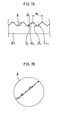
- a light conductive plate 71 has, at its light emit surface, a plurality of polygonal prisms P k ( 1 ⁇ k ⁇ N ) which have an identical cross section with one another, each of which has its inclined surfaces roughened by various micro ridges and grooves extending in the X-axis direction (refer to Fig. 10B).
- each prism surface has a plurality of micro prisms different from one another so that micro surfaces differently inclined relative to the principal virtual plane are irregularly arrayed in the Y-axis direction, whereby the emission direction of the light exiting out from the light exit surface of the light conductive plate 61 is diffused effectively in the Y-axis direction so as to reduce the non-uniformity of brightness distribution in the Y-axis direction.
- the average surface roughness is preferably set to range from 0.1 to 1.0 ⁇ m in terms of a center line average roughness Ra defined by JIS B 0601-1982.
- the distance W k and the inclination angles ( ⁇ k,1 , ⁇ k,2 , ⁇ k,3 and ⁇ k,4 ) of the sides constituting the polygonal prism P k are appropriately set in consideration of brightness distribution uniformity, and workability in die machining to be described later.
- This structure of roughened prism surfaces may be preferably combined with the light conductive plates 71 and 81 shown in Figs.8A and 8B, and Fig. 9, respectively, which will demonstrate an outstanding diffusion effect.
- a light conductive plate is usually formed of one of the aforementioned transparent resin materials, preferably, by injection molding, and a molding die is processed such that a portion for forming the prisms is cut by a cutting tool having an edge geometry corresponding to the prism configuration so as to meet the prism surface arrangement discussed above with a constant cutting depth from the reference surface based on the principal virtual plane.
- the cutting tool has an edge shaped circular with a predetermined curvature. If the cutting tool has a surface adapted to produce a predetermined center line average roughness Ra, the prim surfaces can be provided with micro ridges and grooves extending in one same direction.
- the prism sheet is disposed on the light conductive plate with their respective prism extension directions oriented orthogonal to each other, but their respective prism extension directions may alternatively be off the orthogonal arrangement by about 10 degrees or less.
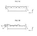
- a molding die for forming a light conductive plate was processed by a cutting tool which has an edge configured with a circular arc with a curvature radius of 35 ⁇ m such that a plurality of grooves are formed with a cutting depth kept constant at 35 ⁇ m from the reference plane and with a feeding distance varied irregularly within a range of 45 to 65 ⁇ m. Tangential angles at respective butting ends of two adjacent circular arcs are equal to each other while overall tangential angles vary irregularly so as to range from 40 to 70 degrees.
- a light conductive plate with its YZ section configured as shown in Fig. 11A was manufactured as an inventive sample. As shown in Fig.
- the prisms on the inventive sample have an identical height h of 35 ⁇ m from the principal virtual plane S.
- a spread illuminating apparatus was produced such that a prism sheet was placed on a light exit surface of the above-described light conductive plate with their respective prism extension directions oriented orthogonal to each other.
- Vibration test (amplitude: 1.5 mm; frequency range: 15 to 60 Hz; cycle: 15 minutes; testing time: 1 hour each in the X, Y and Z directions) and heat cycle test (temperature range: -40 to 85 degrees C; cycle: 1 hour; testing time: 100 hours) were conducted on the spread illuminating apparatus thus produced, and no scratches were found at any parts of the prisms of both the light conductive plate and the prism sheet, including the mutual contact portions thereof. And, it was found that the inventive sample described above shows optical characteristics, such as front brightness and brightness distribution uniformity, equivalent to those of a comparative sample described below.
- a molding die for forming a light conductive plate was processed by a cutting tool which has an edge configured with a circular arc with a curvature radius of 35 ⁇ m such that a plurality of grooves are formed with a cutting depth varied irregularly within a range of 25 to 35 ⁇ m from the reference plane and with a feeding distance varied irregularly within a range of 45 to 65 ⁇ m. Tangential angles at respective butting ends of adjacent two circular arcs are equal to each other while overall tangential angles vary irregularly so as to range from 40 to 70 degrees.
- a light conductive plate with its YZ section configured as shown in Fig. 11B was manufactured as a comparative sample. As shown in Fig.
- the prisms on the comparative sample have respective heights differing irregularly from one another between h1 and h2 (25 to 35 ⁇ m) from the principal virtual plane S.
- Another spread illuminating apparatus was produced such that a prism sheet was placed on a light exit surface of the above-described light conductive plate with their respective prism extension directions oriented orthogonal to each other.
- Vibration test (amplitude: 1.5 mm; frequency range: 15 to 60 Hz; cycle: 15 minutes; testing time: 1 hour each in the X, Y and Z directions) and heat cycle test (temperature range: -40 to 85 degrees C; cycle: 1 hour; testing time: 100 hours) were conducted on the spread illuminating apparatus thus produced, and the mutual contact portions of the prisms of both the light conductive plate and the prism sheet were found to be scratched.
Landscapes
- Physics & Mathematics (AREA)
- General Physics & Mathematics (AREA)
- Optics & Photonics (AREA)
- Planar Illumination Modules (AREA)
- Liquid Crystal (AREA)
- Light Guides In General And Applications Therefor (AREA)
- Optical Elements Other Than Lenses (AREA)
Abstract
Description
Claims (8)
- A spread illuminating apparatus (10) comprising:characterized in that the plurality of prisms of the light conductive plate (11) have respective configurations different from one another in cross section taken along a line orthogonal to the extension direction, wherein respective ridges of the plurality of prisms are located on a common virtual plane.a light conductive plate (11) having a light exit surface (11a) provided with a plurality of prisms which define one extension direction;at least one point light source (12) disposed at a side surface (11c) of the light conductive plate (11); anda prism sheet (13) having a prism surface (13a) provided with a plurality of prisms which define one extension direction, the prism sheet (13) being disposed on the light conductive plate (13) such that the prism surface (13a) faces the light exit surface (11a) of the light conductive plate (11), and that the extension direction of the prisms of the prism sheet (13) is oriented substantially orthogonal to the extension direction of the prisms of the light conductive plate (11),
- A spread illuminating apparatus (10) according to Claim 1, wherein the extension direction of the prisms of the light conductive plate (11) is substantially orthogonal to the side surface (11c) of the light conductive plate (11), at which the at least one point light source (12) is disposed.
- A spread illuminating apparatus (10) according to Claim 1 or 2, wherein the prisms of the light conductive plate (11) are arrayed such that distances each defined between apexes of adjacent two of the prisms differ irregularly from one another.
- A spread illuminating apparatus (10) according to Claim 1 or 2, wherein the prisms of the light conductive plate (11) have respective circular arc configurations with a common curvature in cross section taken the line orthogonal to the extension direction thereof, and wherein two tangential angles at respective butting ends of adjacent two of the prisms of the light conductive plate (11) are equal to each other.
- A spread illuminating apparatus (10) according to Claim 4, wherein overall tangential angles at respective ends of the prisms of the light conductive plate (11) are arranged to vary irregularly within a range of 40 to 70 degrees.
- A spread illuminating apparatus (10) according to Claim 1 or 2, wherein the prisms of the light conductive plate (11) have respective circular arc configurations with a common curvature in cross section taken the line orthogonal to the extension direction thereof, and wherein the prisms of the light conductive plate (11) are arrayed such that distances each defined between apexes of adjacent two of the prisms differ irregularly from one another within a range of 10 to 200 µm.
- A spread illuminating apparatus (10) according to any one of Claims 1 to 6, wherein the prisms of the light conductive plate (11) have their surfaces roughened with micro ridges and grooves extending in one direction parallel to the extension direction of the prisms of the light conductive plate (11).
- A spread illuminating apparatus (10) according to Claim 7, wherein the roughened surfaces of the prisms of the light conductive plate (11) have an average surface roughness of 0.1 to 1.0 µm.
Applications Claiming Priority (2)
| Application Number | Priority Date | Filing Date | Title |
|---|---|---|---|
| JP2004135915 | 2004-04-30 | ||
| JP2004135915A JP4432039B2 (en) | 2004-04-30 | 2004-04-30 | Surface lighting device |
Publications (2)
| Publication Number | Publication Date |
|---|---|
| EP1591826A1 true EP1591826A1 (en) | 2005-11-02 |
| EP1591826B1 EP1591826B1 (en) | 2006-08-16 |
Family
ID=34934241
Family Applications (1)
| Application Number | Title | Priority Date | Filing Date |
|---|---|---|---|
| EP05005456A Ceased EP1591826B1 (en) | 2004-04-30 | 2005-03-14 | Spread illuminating apparatus |
Country Status (4)
| Country | Link |
|---|---|
| US (1) | US7246933B2 (en) |
| EP (1) | EP1591826B1 (en) |
| JP (1) | JP4432039B2 (en) |
| DE (1) | DE602005000071T2 (en) |
Cited By (6)
| Publication number | Priority date | Publication date | Assignee | Title |
|---|---|---|---|---|
| EP1895334A3 (en) * | 2006-08-31 | 2009-09-16 | Rohm and Haas Denmark Finance A/S | Light redirecting film having varying optical elements |
| EP2141521A3 (en) * | 2008-05-15 | 2010-03-03 | LG Electronics Inc. | Light pipe and illuminating device having the same |
| US8057073B2 (en) | 2008-05-07 | 2011-11-15 | Lg Electronics Inc. | Light pipe and illuminating device having the same |
| CN101581435B (en) * | 2008-05-15 | 2011-11-30 | Lg电子株式会社 | Light pipe and illuminating device with the light pipe |
| US8075167B2 (en) | 2008-05-20 | 2011-12-13 | Lg Electronics Inc. | Optical film and illuminating device having the same |
| US8789992B2 (en) | 2008-05-08 | 2014-07-29 | Lg Electronics Inc. | Light pipe and illuminating device having the same |
Families Citing this family (40)
| Publication number | Priority date | Publication date | Assignee | Title |
|---|---|---|---|---|
| US7199868B2 (en) * | 2004-11-02 | 2007-04-03 | Identix Incorporated | High performance fingerprint imaging system |
| US8320645B2 (en) * | 2004-11-02 | 2012-11-27 | Identix Incorporated | High performance multi-mode palmprint and fingerprint scanning device and system |
| US7347610B2 (en) * | 2005-01-26 | 2008-03-25 | Radiant Opto-Electronics Corporation | Light guide plate having light diffusing entities on light entering side |
| TWI255924B (en) | 2005-03-16 | 2006-06-01 | Au Optronics Corp | Backlight module and brightness enhancement film thereof |
| CN101142442A (en) * | 2005-03-17 | 2008-03-12 | 富士通株式会社 | Lighting device and liquid crystal display device |
| TW200641414A (en) * | 2005-05-27 | 2006-12-01 | Innolux Display Corp | Light guide plate and backlight module using the same |
| CN1932602A (en) * | 2005-09-14 | 2007-03-21 | 鸿富锦精密工业(深圳)有限公司 | Light-conducting plate |
| TW200722852A (en) * | 2005-12-06 | 2007-06-16 | Nano Prec Corp | Edge-type backlight module |
| KR20070108794A (en) * | 2006-05-08 | 2007-11-13 | 미래나노텍(주) | Back light assembly of the liquid crystal display device provided with the optical sheet and the optical sheet |
| US20070291510A1 (en) * | 2006-06-15 | 2007-12-20 | Wintek Corporation | Backlight module and light guide plate thereof |
| EP2081059B1 (en) | 2006-11-09 | 2012-08-08 | Sharp Kabushiki Kaisha | Prism sheet and liquid crystal display |
| TW200837452A (en) * | 2007-03-12 | 2008-09-16 | Wintek Corp | Back light module |
| KR100838322B1 (en) * | 2007-03-28 | 2008-06-13 | 제일모직주식회사 | Light guide plate for backlight unit of liquid crystal display device having asymmetric front prism |
| KR100912260B1 (en) * | 2007-03-28 | 2009-08-17 | 제일모직주식회사 | Optical prism sheet for liquid crystal display device having constant roughness on the surface |
| KR100905241B1 (en) * | 2007-04-13 | 2009-07-01 | 엘지전자 주식회사 | Optical film including a plurality of structures and a backlight unit comprising the same |
| US7529461B1 (en) * | 2007-11-20 | 2009-05-05 | Radiant Opto-Electronics Corporation | Light guide plate with compensated emission light field |
| US8721153B2 (en) * | 2007-12-20 | 2014-05-13 | 3M Innovative Properties Company | Backlight reflectors having a prismatic structure |
| KR101421628B1 (en) * | 2008-01-11 | 2014-07-24 | 삼성디스플레이 주식회사 | Back light assembly |
| JP5486504B2 (en) * | 2008-10-22 | 2014-05-07 | 株式会社クラレ | Surface light source element and image display device having the same |
| TWI378300B (en) * | 2008-11-25 | 2012-12-01 | Au Optronics Corp | Light guide plate and backlight module |
| EP2416622B1 (en) | 2009-03-31 | 2019-01-30 | Toppan Printing Co., Ltd. | El panel, and illuminating device and display device using el panel |
| WO2011052739A1 (en) * | 2009-10-30 | 2011-05-05 | 大日本印刷株式会社 | Optical sheet, surface light source apparatus, and transmissive display apparatus |
| JP2012003971A (en) * | 2010-06-17 | 2012-01-05 | Dainippon Printing Co Ltd | Laminated body for plane light source device, plane light source device, and liquid crystal display |
| US8735791B2 (en) | 2010-07-13 | 2014-05-27 | Svv Technology Innovations, Inc. | Light harvesting system employing microstructures for efficient light trapping |
| JP2012068276A (en) * | 2010-09-21 | 2012-04-05 | Oji Paper Co Ltd | Light diffusion sheet |
| US8733999B2 (en) * | 2011-08-23 | 2014-05-27 | Reuven Rahamim | Method and apparatus pertaining to display backlighting |
| US8797480B2 (en) | 2011-10-18 | 2014-08-05 | Dai Nippon Printing Co., Ltd. | Light guide plate, surface light source device, and display device |
| TW201317675A (en) * | 2011-10-20 | 2013-05-01 | Qisda Corp | Backlight module |
| US9671547B2 (en) * | 2012-04-23 | 2017-06-06 | Sharp Kabushiki Kaisha | Illumination device and display device |
| KR102080276B1 (en) * | 2013-05-23 | 2020-02-21 | 엘지디스플레이 주식회사 | Back Light Unit and Liquid Crystal Display Device using the same |
| TW201426037A (en) * | 2012-12-26 | 2014-07-01 | Hon Hai Prec Ind Co Ltd | Light guide plate and making method thereof |
| TWI472817B (en) * | 2013-04-30 | 2015-02-11 | Radiant Opto Electronics Corp | A light guide means and a backlight module having the light guide means |
| EP3012519B1 (en) * | 2013-06-13 | 2017-11-29 | Kuraray Co., Ltd. | Lighting device |
| US9239420B2 (en) * | 2013-07-26 | 2016-01-19 | Dai Nippon Printing Co., Ltd. | Light guide plate, surface source device and transmission-type display device |
| JP5765647B2 (en) * | 2014-03-11 | 2015-08-19 | 大日本印刷株式会社 | Light guide plate, surface light source device and display device |
| US9798066B2 (en) * | 2014-08-18 | 2017-10-24 | New Optics, Ltd | Display device and light guide plate thereof |
| US9684116B2 (en) * | 2014-08-18 | 2017-06-20 | New Optics, Ltd | Light guide plate, and backlight unit and display device including the same |
| CN106523986A (en) * | 2016-10-31 | 2017-03-22 | 马瑞利汽车零部件(芜湖)有限公司 | Light curtain automobile tail light with gradual change effect |
| KR102079427B1 (en) * | 2017-10-25 | 2020-02-19 | 부산대학교 산학협력단 | Apparatus for making interference patterns on the inclined surface |
| JP7414621B2 (en) * | 2020-04-03 | 2024-01-16 | 株式会社ジャパンディスプレイ | Light emitting device and lighting device |
Citations (2)
| Publication number | Priority date | Publication date | Assignee | Title |
|---|---|---|---|---|
| JP2004006326A (en) * | 2002-04-22 | 2004-01-08 | Mitsubishi Rayon Co Ltd | Surface light source device and light guide used therein |
| US20040120139A1 (en) * | 2002-12-19 | 2004-06-24 | Minebea Co., Ltd. | Spread illuminating apparatus with light scattering means |
Family Cites Families (6)
| Publication number | Priority date | Publication date | Assignee | Title |
|---|---|---|---|---|
| JPH10253960A (en) | 1997-03-14 | 1998-09-25 | Enplas Corp | Sidelight type surface light source device and light control member |
| WO2000008494A1 (en) * | 1998-08-05 | 2000-02-17 | Mitsubishi Rayon Co., Ltd. | Lens sheet and method for producing the same |
| KR20020041431A (en) * | 2000-07-11 | 2002-06-01 | 미우라 아키라 | Surface light source device |
| JP2002050219A (en) * | 2000-07-25 | 2002-02-15 | Internatl Business Mach Corp <Ibm> | Planar light source device, light guide plate, display device |
| US6576887B2 (en) * | 2001-08-15 | 2003-06-10 | 3M Innovative Properties Company | Light guide for use with backlit display |
| US7052168B2 (en) * | 2003-12-17 | 2006-05-30 | 3M Innovative Properties Company | Illumination device |
-
2004
- 2004-04-30 JP JP2004135915A patent/JP4432039B2/en not_active Expired - Fee Related
-
2005
- 2005-03-09 US US11/074,700 patent/US7246933B2/en not_active Expired - Lifetime
- 2005-03-14 EP EP05005456A patent/EP1591826B1/en not_active Ceased
- 2005-03-14 DE DE602005000071T patent/DE602005000071T2/en not_active Expired - Lifetime
Patent Citations (2)
| Publication number | Priority date | Publication date | Assignee | Title |
|---|---|---|---|---|
| JP2004006326A (en) * | 2002-04-22 | 2004-01-08 | Mitsubishi Rayon Co Ltd | Surface light source device and light guide used therein |
| US20040120139A1 (en) * | 2002-12-19 | 2004-06-24 | Minebea Co., Ltd. | Spread illuminating apparatus with light scattering means |
Non-Patent Citations (1)
| Title |
|---|
| PATENT ABSTRACTS OF JAPAN vol. 2003, no. 12 5 December 2003 (2003-12-05) * |
Cited By (7)
| Publication number | Priority date | Publication date | Assignee | Title |
|---|---|---|---|---|
| EP1895334A3 (en) * | 2006-08-31 | 2009-09-16 | Rohm and Haas Denmark Finance A/S | Light redirecting film having varying optical elements |
| US8057073B2 (en) | 2008-05-07 | 2011-11-15 | Lg Electronics Inc. | Light pipe and illuminating device having the same |
| US8789992B2 (en) | 2008-05-08 | 2014-07-29 | Lg Electronics Inc. | Light pipe and illuminating device having the same |
| EP2141521A3 (en) * | 2008-05-15 | 2010-03-03 | LG Electronics Inc. | Light pipe and illuminating device having the same |
| US7748874B2 (en) | 2008-05-15 | 2010-07-06 | Lg Electronics Inc. | Light pipe and illuminating device having the same |
| CN101581435B (en) * | 2008-05-15 | 2011-11-30 | Lg电子株式会社 | Light pipe and illuminating device with the light pipe |
| US8075167B2 (en) | 2008-05-20 | 2011-12-13 | Lg Electronics Inc. | Optical film and illuminating device having the same |
Also Published As
| Publication number | Publication date |
|---|---|
| JP2005317435A (en) | 2005-11-10 |
| JP4432039B2 (en) | 2010-03-17 |
| DE602005000071T2 (en) | 2007-03-15 |
| US20050243575A1 (en) | 2005-11-03 |
| EP1591826B1 (en) | 2006-08-16 |
| DE602005000071D1 (en) | 2006-09-28 |
| US7246933B2 (en) | 2007-07-24 |
Similar Documents
| Publication | Publication Date | Title |
|---|---|---|
| EP1591826B1 (en) | Spread illuminating apparatus | |
| US7452120B2 (en) | Illumination apparatus and film | |
| KR100678850B1 (en) | Surface light source device, diffuser plate and liquid crystal display device | |
| US7775700B2 (en) | Turning film using array of roof prism structures | |
| KR101257674B1 (en) | Surface light source element and image display device provided with the surface light source element | |
| EP0940706B1 (en) | Transparent front-surface illuminating apparatus in a liquid crystal display | |
| US7458713B2 (en) | Illumination device and light guide plate | |
| US7972052B2 (en) | Backlight unit | |
| US20070274097A1 (en) | Backlight module and light guide plate thereof | |
| US20040161222A1 (en) | Optical waveguide, area light source device and liquid crystal display device | |
| KR20110086067A (en) | Surface light source element and image display apparatus provided with the same | |
| JP2010135326A (en) | Light guide plates, and backlight module | |
| JP2011100724A (en) | Image display device | |
| EP1602949B1 (en) | Spread illuminating apparatus | |
| US7139464B2 (en) | Surface light source and light guide used therefor | |
| US7178966B2 (en) | Light guide plate with nonuniformly oriented diffusing elements | |
| JPWO2008066154A1 (en) | Surface light source element and image display device including the same | |
| US20070223249A1 (en) | Light redirecting film | |
| KR20060043378A (en) | LGP, surface light emitting device using LGP and manufacturing method | |
| JPH1073820A (en) | Non-light-diffusing light guide plate, lens film, and surface light source device | |
| KR20030080764A (en) | A Direct-lighting Backlight Unit | |
| JP5644413B2 (en) | Light guide, surface light source device, and image display device | |
| JP2001210123A (en) | Surface light source device and method of manufacturing the same | |
| JP4984512B2 (en) | Surface light emitting device and liquid crystal display device | |
| JP2009140743A (en) | Light guide plate and surface light emitting device using the same |
Legal Events
| Date | Code | Title | Description |
|---|---|---|---|
| PUAI | Public reference made under article 153(3) epc to a published international application that has entered the european phase |
Free format text: ORIGINAL CODE: 0009012 |
|
| AK | Designated contracting states |
Kind code of ref document: A1 Designated state(s): AT BE BG CH CY CZ DE DK EE ES FI FR GB GR HU IE IS IT LI LT LU MC NL PL PT RO SE SI SK TR |
|
| AX | Request for extension of the european patent |
Extension state: AL BA HR LV MK YU |
|
| GRAP | Despatch of communication of intention to grant a patent |
Free format text: ORIGINAL CODE: EPIDOSNIGR1 |
|
| 17P | Request for examination filed |
Effective date: 20060112 |
|
| GRAS | Grant fee paid |
Free format text: ORIGINAL CODE: EPIDOSNIGR3 |
|
| AKX | Designation fees paid |
Designated state(s): DE FI FR GB |
|
| GRAA | (expected) grant |
Free format text: ORIGINAL CODE: 0009210 |
|
| AK | Designated contracting states |
Kind code of ref document: B1 Designated state(s): DE FI FR GB |
|
| REG | Reference to a national code |
Ref country code: GB Ref legal event code: FG4D |
|
| REF | Corresponds to: |
Ref document number: 602005000071 Country of ref document: DE Date of ref document: 20060928 Kind code of ref document: P |
|
| ET | Fr: translation filed | ||
| PLBE | No opposition filed within time limit |
Free format text: ORIGINAL CODE: 0009261 |
|
| STAA | Information on the status of an ep patent application or granted ep patent |
Free format text: STATUS: NO OPPOSITION FILED WITHIN TIME LIMIT |
|
| 26N | No opposition filed |
Effective date: 20070518 |
|
| REG | Reference to a national code |
Ref country code: FR Ref legal event code: PLFP Year of fee payment: 12 |
|
| REG | Reference to a national code |
Ref country code: FR Ref legal event code: PLFP Year of fee payment: 13 |
|
| REG | Reference to a national code |
Ref country code: DE Ref legal event code: R082 Ref document number: 602005000071 Country of ref document: DE Representative=s name: LEDERER & KELLER PATENTANWAELTE PARTNERSCHAFT , DE Ref country code: DE Ref legal event code: R081 Ref document number: 602005000071 Country of ref document: DE Owner name: MINEBEA MITSUMI INC., JP Free format text: FORMER OWNER: MINEBEA CO., LTD., MIYOTA-MACHI, NAGANO-GUN, JP |
|
| REG | Reference to a national code |
Ref country code: FR Ref legal event code: PLFP Year of fee payment: 14 |
|
| PGFP | Annual fee paid to national office [announced via postgrant information from national office to epo] |
Ref country code: DE Payment date: 20180227 Year of fee payment: 14 Ref country code: FI Payment date: 20180312 Year of fee payment: 14 Ref country code: GB Payment date: 20180314 Year of fee payment: 14 |
|
| PGFP | Annual fee paid to national office [announced via postgrant information from national office to epo] |
Ref country code: FR Payment date: 20180223 Year of fee payment: 14 |
|
| REG | Reference to a national code |
Ref country code: DE Ref legal event code: R119 Ref document number: 602005000071 Country of ref document: DE |
|
| PG25 | Lapsed in a contracting state [announced via postgrant information from national office to epo] |
Ref country code: FI Free format text: LAPSE BECAUSE OF NON-PAYMENT OF DUE FEES Effective date: 20190314 |
|
| GBPC | Gb: european patent ceased through non-payment of renewal fee |
Effective date: 20190314 |
|
| PG25 | Lapsed in a contracting state [announced via postgrant information from national office to epo] |
Ref country code: GB Free format text: LAPSE BECAUSE OF NON-PAYMENT OF DUE FEES Effective date: 20190314 Ref country code: DE Free format text: LAPSE BECAUSE OF NON-PAYMENT OF DUE FEES Effective date: 20191001 |
|
| PG25 | Lapsed in a contracting state [announced via postgrant information from national office to epo] |
Ref country code: FR Free format text: LAPSE BECAUSE OF NON-PAYMENT OF DUE FEES Effective date: 20190331 |