EP1589394A1 - Microprocesseur comprenant des moyens de détection d'erreur immunisés contre une attaque par injection d'erreur - Google Patents
Microprocesseur comprenant des moyens de détection d'erreur immunisés contre une attaque par injection d'erreur Download PDFInfo
- Publication number
- EP1589394A1 EP1589394A1 EP05007485A EP05007485A EP1589394A1 EP 1589394 A1 EP1589394 A1 EP 1589394A1 EP 05007485 A EP05007485 A EP 05007485A EP 05007485 A EP05007485 A EP 05007485A EP 1589394 A1 EP1589394 A1 EP 1589394A1
- Authority
- EP
- European Patent Office
- Prior art keywords
- signature
- execution
- circuit
- sequence
- signals
- Prior art date
- Legal status (The legal status is an assumption and is not a legal conclusion. Google has not performed a legal analysis and makes no representation as to the accuracy of the status listed.)
- Granted
Links
Images
Classifications
-
- G—PHYSICS
- G06—COMPUTING OR CALCULATING; COUNTING
- G06F—ELECTRIC DIGITAL DATA PROCESSING
- G06F21/00—Security arrangements for protecting computers, components thereof, programs or data against unauthorised activity
- G06F21/50—Monitoring users, programs or devices to maintain the integrity of platforms, e.g. of processors, firmware or operating systems
- G06F21/52—Monitoring users, programs or devices to maintain the integrity of platforms, e.g. of processors, firmware or operating systems during program execution, e.g. stack integrity ; Preventing unwanted data erasure; Buffer overflow
-
- G—PHYSICS
- G06—COMPUTING OR CALCULATING; COUNTING
- G06F—ELECTRIC DIGITAL DATA PROCESSING
- G06F21/00—Security arrangements for protecting computers, components thereof, programs or data against unauthorised activity
- G06F21/70—Protecting specific internal or peripheral components, in which the protection of a component leads to protection of the entire computer
- G06F21/71—Protecting specific internal or peripheral components, in which the protection of a component leads to protection of the entire computer to assure secure computing or processing of information
-
- G—PHYSICS
- G01—MEASURING; TESTING
- G01R—MEASURING ELECTRIC VARIABLES; MEASURING MAGNETIC VARIABLES
- G01R31/00—Arrangements for testing electric properties; Arrangements for locating electric faults; Arrangements for electrical testing characterised by what is being tested not provided for elsewhere
- G01R31/28—Testing of electronic circuits, e.g. by signal tracer
- G01R31/317—Testing of digital circuits
- G01R31/31719—Security aspects, e.g. preventing unauthorised access during test
Definitions
- the present invention relates to the protection of microprocessor integrated circuits against attacks by injection of error.
- the present invention relates more particularly a method for monitoring execution a sequence of code-instructions in a circuit integrated system comprising a central processing unit planned to execute such instruction codes, as well as an integrated circuit of the aforementioned type comprising means of monitoring the performance of at least one sequence of instruction codes comprising at least one instruction code.
- the detection of the injections of error is considered an essential measure to guarantee a high level of security to certain integrated circuits, particularly integrated circuits for smart cards.
- the present invention is based on the finding according to which the execution of instruction codes by the central processing unit (CPU) of an integrated circuit microprocessor involves various signals that are sometimes deterministic, ie predictable, and sometimes non-deterministic.
- the structure of microprocessor being known to the manufacturer and generally of the professional user, it is possible to draw up an inventory, for each code-instruction executed, signals that are of the deterministic type among all the signals of address, control or data involved in the execution of the code-instruction, and to produce signatures from such signals.
- operand type data read in a ROM as a ROM, or in areas write-protected erasable memory and programmable electrically are data deterministic.
- deterministic addresses traveling on an address bus during the execution of codes-instructions, including the reading addresses of the code-instructions themselves ("fetch" cycles), as well as operand addresses.
- deterministic control signals appearing in the microprocessor during execution instruction codes for example read / write, memory select signals or registers, and signals indicating that the unit Central performs a specific operation.
- a first idea of the present invention is to monitor the execution of a sequence of instruction codes comprising at least one code-instruction in producing cumulative signatures from a plurality of deterministic signals intervening in the execution of the instruction code (s), and to compare a final signature obtained at an expected signature.
- an expected signature can be determined by the programmer since it relies only on signals deterministic and on sequences of operations deterministic.
- the aim pursued by such monitoring of the execution of a program is, well heard, to issue an error signal with a value active when an anomaly is detected.
- active value the fact that the error signal, when presents this value, triggers operations necessary for the protection of the integrated circuit, example the application of a reset signal to the central unit, or the provision of a signal interrupt that switches the CPU into a determined subprogram, the destruction of data sensitive elements present in a memory, etc., these various protection operations are in themselves well known to the skilled person.
- a error signal is generated when the program reaches a final statement of verification of the signature, that closes the execution of the sequence of code-instructions under surveillance.
- the final instruction to verify the signature is not executed and the error signal is not output.
- a second idea of the present invention is to provide an error signal that defaults to the value active and can only be neutralized that a final signature obtained after the execution of a code sequence instructions equal to a signature expected.
- Such an error signal is masked during execution of operations to be controlled, and masking is lifted unconditionally after a lapse time corresponding substantially to the execution time operations to be controlled. If the error signal does not been neutralized by the appearance of a valid signature when the masking is lifted, it becomes active in the integrated circuit since it is no longer masked.
- the present invention provides a method for monitoring the execution of a sequence of instruction codes in an integrated circuit including a central processing unit intended for execute such instruction codes, including the steps of: during the execution of the sequence, produce common cumulative signatures that are function of logic signals taken from the circuit integrated, until, at the end of the execution of the sequence, a final cumulative signature; while execution of the sequence, produce an error signal default value is active and remains at the value active as long as the current cumulative signature is different from an expected signature; hide the signal error during a predetermined time interval corresponding substantially to the duration of execution presumed sequence, and unconditionally lift the hiding the error signal on the expiration of the predetermined time interval.
- the time interval predetermined is measured by a timer that is activated by the central unit before the start of execution of the sequence and that emits a signal that changes value when the timer has finished measuring the interval of time, and the masking of the error signal is ensured by a logic circuit that is transparent or non-transparent vis-à-vis the error signal according to the value of the signal issued by the timer.
- each signature cumulative current is produced in synchronization with a clock signal according to a signature previous cumulative and logical signals determinists of address, control or data involved in the execution of the sequence.
- the clock signal which rhythm the production of signatures is the signal clock of the CPU, and a signature cumulative current is produced at each clock cycle of the CPU during the execution of the sequence.
- the logic signals according to which current cumulative signatures are produced include all or part of the signals following: addresses applied to elements peripherals of the central unit, signals from control of peripheral elements, signals indicative of ongoing operations, data forming operands or code-instructions, and a signal is excluded from the calculation of a cumulative signature if it is not deterministic during the clock cycle during which the signature is produced.
- the signatures cumulative results are produced by means of a calculation of hard-wired logic signatures including parallel inputs connected to circuit points integrated, and inputs to the computing circuit of signatures are inhibited by means of a circuit of configurable wired logic masking, to exclude non-deterministic signals.
- the inputs of the signature calculation circuit are connected to a bus data, an address bus, and a control bus which conveys element control signals peripherals of the central unit.
- the calculation of cumulative signatures is made by means of a linear feedback shift register.
- the present invention also relates to a circuit integrated system comprising a central processing unit for execute a program including instruction codes, and means of monitoring the performance of at least a code-instruction sequence comprising at least one code-instruction, in which the means of supervision include a signature calculation circuit for produce common cumulative signatures that are function of logic signals taken from the circuit integrated, the signature calculation circuit providing, at the end of the execution of the sequence, a signature cumulative, a means of memorizing a expected signature, a timer to measure a predetermined time interval, means for produce an error signal that defaults to a value active from the beginning of the execution of the sequence, and staying at the active value as long as the signature cumulative current is different from the signature expected, and means to hide the error signal during the measurement of the time interval by the timer, and unconditionally lift the signal error when the time interval expires.
- the means of supervision include a signature calculation circuit for produce common cumulative signatures that are function of logic signals taken from the circuit integrated, the signature calculation circuit providing, at the end of the execution of the sequence
- the integrated circuit includes a logic signal masking circuit error, receiving on an input the error signal and on another input a signal provided by the timer, the masking logic circuit being transparent or not transparent to the error signal according to the value the signal emitted by the timer.
- the integrated circuit comprises a comparator receiving on an input current cumulative signature and on another entry the expected signature, and a memory element such a flip-flop to provide the error signal, arranged to disable the error signal when the output of the comparator indicates equal signatures.
- the integrated circuit comprises a comparator receiving on an input current cumulative signature and on another entry the expected signature, whose output provides the signal error, and means to execute an instruction of deactivation of the signature calculation circuit.
- the calculation circuit of signatures includes parallel entries connected in various points of the integrated circuit through which logical signals of address, control or data intervening in the execution of the sequence and to be deterministic, and a logical masking circuit wired configurable is arranged in front of the inputs of the signature calculation circuit to inhibit inputs likely to receive non-deterministic signals during the execution of the sequence.
- the circuit of configurable masking includes a register accessible to the less in writing to receive a string of bits forming a binary mask.
- the calculation circuit of signatures includes entries related to points of the integrated circuit where all or part of the following signals: addresses applied to elements peripherals of the central unit, signals from control of peripheral elements, signals indicative of ongoing operations, data forming operands or code-instructions.
- the calculation circuit of signatures includes inputs connected to a bus of data, inputs connected to an address bus, and inputs connected to a control bus on which transit element control signals peripherals of the central unit.
- the calculation circuit of signatures is clocked by a clock signal of the CPU, and calculates a cumulative signature current at each clock cycle, replacing each previous signature by a new signature, in a storage register of the current signature.
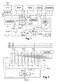
- Figure 1 shows the architecture of a circuit integrated microprocessor type IC or microcontroller, equipped with a monitoring device according to the invention.
- a monitoring device makes it possible to monitor the operation of the integrated circuit during the execution of a sequence of codes-instructions to detect, in particular, a error injection.
- the integrated circuit IC conventionally comprises a CPU (CPU) and elements CPU peripherals, here memories MEM1, MEM2, MEM3 and a REGBANK register bank. Other elements peripherals may be provided, not shown here, in particular a cryptographic calculation circuit.
- the memory MEM1 is for example a non-volatile memory of type ROM (read only memory), the memory MEM2 a memory electrically erasable and programmable type EEPROM, and the memory MEM3 a volatile memory type RAM.
- the memory MEM1 contains, for example, master programs (programs developed by the manufacturer: test, security management, authentication ...) and operands.
- the memory MEM2 comprises, for example application programs (programs developed by the user) and operands. These various programs are composed of instruction codes executable by the CPU.
- the memory MEM3 generally contains data application, which disappear when the integrated circuit is off.
- the REGBANK register bank can contain volatile data like variables, calculation results, flags, etc.
- Control bus is defined as a set of wires conveying selection or information signals issued by the CPU to the attention of peripheral elements, or vice versa.
- the CB bus carries signals in particular SEL1, SEL2, SEL3 for selecting memories MEM1, MEM2, MEM3, a signal SEL4 for selecting the bank of REGBANK registers, an R / W signal for reading or writing, as well as a FETCH signal issued by the CPU during the reading a code-instruction in one of the memories program MEM1, MEM2.
- the monitoring device comprises a signature production circuit 10 and a error detection circuit 20, delimited by dashed lines in Figure 1.
- Each circuit 10, 20 is in itself independent of the other and corresponds to a aspect of the present invention. So, like this will appear on reading the following, the circuit 10 can be combined with an error detection circuit other than the circuit 20 shown, and vice versa.
- the signature production circuit 10 firstly comprises a circuit calculation circuit SCCT hardwired logic.
- the circuit SCCT comprises parallel inputs I1, I2, I3 and is clocked by a clock signal CK1 which is preferably the clock signal of the CPU.
- the SCCT circuit is for example a conventional LSFR register (Linear Feedback Shift Register), or a linear feedback shift register.
- the circuit SCCT comprises a logic circuit PLCT and a signature register SREG with input and output of parallel type.
- the circuit PLCT executes a signature function Fs and comprises inputs I1, I2, I3 forming the inputs of the circuit SCCT, and an input I4 receiving a current cumulative signature CCS.
- the inputs I1, I2, I3 of the circuit SCCT are connected to various points of the integrated circuit through which address, control or data signals intervene in the execution of the instruction codes present in the memories MEM1. , MEM2, and receive groups G1, G2, G3 of signature generating signals.
- the input I1 is connected to the data bus DB
- the input I2 is connected to the address bus AB
- the input I3 is connected to the control bus CB.
- the group of signals G1 comprises N data bits d 0 , d 1 , .. d N-1 taken from the data bus, which are applied to N elementary inputs I1 0 , I1 1 , ... I1 N- 1 forming the input I1.
- the group of signals G2 comprises N address bits at 0 , a 1 ... a M-1 taken from the address bus and applied to N elementary inputs I2 0 , I2 1 , ... I2 M-1 forming the entry I2.
- the group of signals G3 comprises K control signals c 0 , c 1 ... C k-1 taken on the control bus and applied to N elementary inputs I3 0 , I3 1 , ... I3 k-1 forming the entry 13.
- FETCH read operation
- signals may also not be deterministic, in whole or in part.
- a variable calculated according to a given data or unpredictable event is a variable that is itself unpredictable.
- reading of such variable in a memory for example in the memory MEM3 (RAM) or in the register bank, although that not being deterministic with respect to the value of the variable itself, can be predictable with respect to the read address of the variable if this address was determined by the programmer and lies so fixed by the program, and does not depend on result of a calculation involving a parameter or unpredictable data.
- the signals taken from the data bus, ie the signals forming group G1 are not deterministic, while the address signals forming the group G2 and the signals of control group G3 are.
- the inputs I1, I2, I3 of the SSCT signature calculation circuit are connected to the buses DB, AB, CB via a masking circuit at configurable wired logic controller whose configuration is provided by a CONFREG register.
- the CONFREG register is accessible at least in writing, preferably in read / write, via the data bus DB, and is connected to the control bus for selection in reading and / or writing.
- the register CONFREG receives a string of bits forming a binary mask, constituted here of three distinct binary masks M1, M2, M3 concatenated.
- the mask M1 is designed to mask all or part of the elementary inputs of the input I1 and comprises N bits m1 0 ' m1 1 ... m1 N-1 .
- the mask M2 is designed to mask all or part of the elementary inputs of the input I2 and comprises M bits m2 0 , m2 1 ... m2 M-1 .
- the mask M3 is designed to mask all or part of the elementary inputs of the input I3 and comprises K bits m3 0 , m3 1 ... m3 K-1 .
- Each mask bit is thus associated with one of the signature generating signals d 0 to d N-1 , a 0 to a M-1 , C 0 to C k-1 , respectively, that it makes it possible to mask or not .
- the register CONFREG thus makes it possible to inhibit, among the N + M + K inputs of the circuit SCCT, those which receive, during a sequence of production of signatures, signature generating signals which are not deterministic.
- the masking is performed physically in the circuit CLM by means of a plurality of AND gates each receiving on one input one of the signals d 0 to d N-1 , a 0 to a M-1 , c 0 to c K- 1 and on another input the corresponding mask bit m1 0 to m1 N-1 , m2 0 to 2 M-1 , m3 0 to m3 k-1 , the output of each AND gate being applied to the corresponding elementary input I1 0 to I1 N-1 , I2 0 to I2 M-1 , I3 0 to I3 K-1 of the SCCT circuit.
- CCS Fs (PCS, G1 * M1, G2 * M2, G3 * M3) "*" here being the AND function
- a 0 bit in the bit mask inhibits the signal generator signature of corresponding rank in forcing its value to 0.
- Any other muting function combinatorics can however be used, for example the function OR, NO OR, NO AND, etc. Switches driven by the bits of the bit mask can also be used as means of inhibition.
- each deterministic sequence includes at least one instructional code or a predictable sequence of instruction codes.
- part of program including a conditional jump instruction which is a function of unpredictable data is not a deterministic sequence.
- Such a sequence must then to be divided into deterministic sequences of smaller cut.
- the execution of each sequence determinist uses signals of address, control or data some of which are deterministic and others are not, as explained above. he should not be confused deterministic of a sequence on which, for example, the described by EP 1 161 725, and the character deterministic signals involved in the execution of the deterministic sequence on which this invention.
- the bit mask loaded in the register CONFREG only has bits at 1 because the sequence at execute only includes deterministic signals, which he this is the read or write address of the operand, the value of the operand (operand known because present in ROM) or control signals.
- the resetting of the SREG register effect of placing in it an initial signature which form the starting value (or base value) for the calculation of cumulative signatures. This initial value can also be chosen non-zero, provided that it is known to the programmer so that he can determine the signature expected at the end of the execution of the sequence, as will be described later.
- the AD_code1 and AD_code2 addresses are the read addresses of the two instruction codes of the secure sequence, provided by a PC program counter of the central unit, not shown in the figures.
- the R / W signal is here to 1 to trigger a reading and to 0 for a write.
- the values marked "xxx" are default values of the data or address bus when a data or a code does not transit on the bus. Such default values are deterministic and are involved in the calculation of the current signature during the relevant clock cycle.
- control signals IN_ALU and OUT_ALU indicate that the CPU performs an internal operation of loading or respectively reading of operand in its arithmetic and logical unit ALU (not shown in the figures). Such control signals are not present on the control bus and are therefore not taken into account in the signature calculation. However, these signals, as well as other internal signals of the CPU, could also be "externalized” like the FETCH signal, in order to be taken into account in the signature calculation.
- a signature cumulative is produced.
- the final cumulative signature obtained is the CCS8 signature.
- This signature is predictable and is so presumed equal to an expected signature WS determined by the programmer at the time the program is designed, preferably by means of a software tool of signature calculation.
- the comparison of the signature final with the expected signature is provided by the error detection circuit 20 which will be now described.
- the AD2 address of loading the operand into the register bank depends on the result of a non-deterministic operation performed by a part of the program preceding the secure sequence. The sequence then becomes semi-deterministic.
- the signals on the address bus are not taken into account during cycles 1 to 8 for the computation of the cumulative signatures, because the address AD2 which is applied on the address bus during cycles 7 and 8 is not predictable.
- the semi-deterministic sequence can also be split into two secure sub-sequences individually, one being entirely deterministic and formed by cycles 1 to 4 (execution of the first code-instruction), the other being semi-deterministic and formed by cycles 5 to 8 (execution of the second code-instruction).
- a first cumulative final signature calculated during cycles 1 to 4 by bringing to 1 all mask bits, is produced at the end of cycle 4 and is compared to a first expected signature.
- a second final cumulative signature calculated during cycles 5 to 8 by setting to 0 the binary mask M2 and to 1 the masks M1, M3, is produced at the end of cycle 8 and is compared to a second expected signature.
- this first aspect of the present invention is susceptible various variants and embodiments, in particular as regards the extent, nature and number of signature generating signals taken into account for produce cumulative signatures.
- the method of the invention can also include stages of production of signatures clocked by a clock signal slower than the clock signal of the CPU, for example producing a signature every two or three clock cycles of the CPU.
- stages of production of signatures clocked by a clock signal slower than the clock signal of the CPU, for example producing a signature every two or three clock cycles of the CPU.
- the error detection circuit 20 shown in FIG. is a wired logic circuit that is autonomous vis-à-vis the CPU except for initialization and its activation.
- the error detection circuit 20 comprises a register REFREG, a comparator COMP, a rocker synchronous FF type flip-flop (or D flip-flop) and a timer TMR ("timer").
- the REFREG register is accessible in reading, from read / write preference, via the DB data bus, and is selected by means of a control bus wire CB. It is intended to receive the expected signature WS calculated by the programmer.
- the timer TMR is a down counter equipped with a CREG counting register accessible in writing, and read / write preference via the DB data bus.
- the timer is clocked by a clock signal CK0, for example a primary clock signal of the circuit integrated from which the clock signal CK1 is product.
- the timer is connected to the CB control bus for selecting the CREG read / write register as well as for activating the timer.
- the timer decrements the CREG register and provides a signal of TS output that is 0. This signal goes to 1 when the CREG register value reaches zero.
- the interval of measured time is thus equal to CVAL / T, T being the period the clock signal CK0.
- the COMP comparator has a first entry linked to the exit of the REFREG register, which receives the signature expected WS, and a second entry connected to the output of the SREG register of the production circuit of signatures 10, which receives the cumulative signature current CCS.
- the COMP comparator output is at 0 that the current signature is different from the signature expected, and goes to 1 when the signatures are equal.
- the flip-flop FF has an input D, an input of synchronization H, an inverted output / Q that provides a ERS error signal, and a reset RST input.
- Input D always receives logic value 1 and input H is connected to the output of comparator COMP.
- the output / Q copies the entry D inverting its value when a rising edge appears on input H.
- the input RST is connected to a CB control bus wire so that the resetting of the flip-flop FF intervenes automatically when an expected WS signature is loaded in the REFREG register.
- the value "1" of the error signal is an active value that causes a stop or reset zero of the CPU or any other known emergency measure of the skilled person. So, the error signal is by defaults to the active value and is not inhibited (change to 0) that if a current signature coincides, at a moment given, with the expected signature WS.
- the error signal ERS is applied to a circuit 30 error management via a door AG logic of type ET which forms a signal mask error.
- the gate AG receives the error signal ERS on one input and the timer signal TS on another input, and its output is applied by means of the error handling 30.
- the circuit 30 is of any known type, for example an interrupt decoder providing a signal of interruption, a circuit of reset of the circuit integrated, a device that automatically erases confidential data present in the EEPROM (MEM2), etc.
- the error signal ERS provides through the gate AG at circuit 30 is forced to 0 by the timer signal TS until the timer has finished counting down the CVAL instruction.
- the masking of the error signal is raised when the TS signal goes to 1.
- the output of the gate AG goes to 1 and the circuit 30 is activated.
- the parameterization and the activation of the error detection circuit 20 include the insertion of specific instructions in the program executed by the CPU, in particular instructions for loading the counting instruction.
- CVAL loading the expected signature WS and activating the timer.
- a sequence incorporating such instructions is for example as indicated below, taking again the example described above: ⁇ loading the counting instruction into the timer CREG register> [LOAD TMR] [CVAL] ⁇ timer activation> [TMR ON] ⁇ load the expected WS signature in the REFREG register> [LOAD REFREG] [WS] ⁇ loading masks M1, M2, M3 in the CONFREG register> [LOAD CONFREG] [M1, M2, M3] ⁇ setting the SREG register to 0> [RESET SREG] ⁇ execution of the secure sequence> [READ MEM1] [AD1] [WRITE REGBANK] [AD2]
- the CVAL counting instruction loaded into the timer is determined taking into account the time execution of the loading instructions of the WS signature, loading the M1-M3 masks and resetting the SREG signature register because these instructions interpose here between instruction timer activation and instructions forming secure sequence itself.
- the provision of error signal is immune to a possible program derailment.
- the secure sequence is not followed by a comparison instruction of signatures, such a comparison being made in time real and hardware. So, if an injection of fault derails the program during the execution of the secure sequence, the current signature is never equal to the expected signature and the management circuit error 30 is activated when the masking time is expired.
- the integrated circuit according to the invention is put by default in an error mode that is temporarily hidden by the timer, which is a potential error, and automatically switches to a unmasked error mode, an active error mode, when the time interval measured by the timer expires, unless in the meantime the current signature is become equal to the expected signature.
- the flip-flop FF is suppressed, the error signal ERS is supplied directly by the comparator COMP and start and stop means of the signature calculation circuit SCCT is provided.
- This means of starting and stopping is for example a switch means controlled by software, which makes it possible to inhibit the application of the clock signal CK1 to the circuit SCCT.
- Codes and instructions for starting and stopping the SCCT circuit are also provided, for example codes START SCCT and STOP SCCT, and are inserted into the program, respectively before and after the sequence to be secured.
- the calculation of the expected signature in this case take into account operations that the CPU performs before the actual stopping of the SCCT circuit. he These include the instructional reading cycles STOP SCCT (fetch cycles) that occur before the actual execution of the instruction code.
Landscapes
- Engineering & Computer Science (AREA)
- Computer Security & Cryptography (AREA)
- Theoretical Computer Science (AREA)
- Software Systems (AREA)
- Computer Hardware Design (AREA)
- Physics & Mathematics (AREA)
- General Engineering & Computer Science (AREA)
- General Physics & Mathematics (AREA)
- Mathematical Physics (AREA)
- Storage Device Security (AREA)
- Debugging And Monitoring (AREA)
Abstract
Description
- la figure 1 représente un circuit intégré à microprocesseur comprenant un dispositif de surveillance selon l'invention, représenté sous forme de blocs, et
- la figure 2 est une vue détaillée d'un circuit de production de signatures représenté sous forme de blocs en figure 1.
- la valeur de l'opérande qui est lue dans la mémoire, de sorte que les signaux apparaissant sur le bus de données (bits de l'opérande), formant le groupe G1, sont déterministes,
- l'adresse de lecture de l'opérande, de sorte que l'ensemble des signaux du groupe G2 apparaissant sur le bus d'adresse sont également déterministes, et
- le signal de sélection de la mémoire MEM1 et le signal de lecture R/W apparaissant sur le bus de contrôle, de sorte que l'ensemble des signaux du groupe G3 sont déterministes (les autres signaux de contrôle étant supposés inactifs, donc ayant également une valeur logique déterminée).
[READ MEM1] [AD1]
[WRITE REGBANK] [AD2]
<chargement des masques M1, M2, M3 dans le registre CONFREG>
[LOAD CONFREG][M1, M2, M3]
<mise à 0 du registre SREG>
[RESET SREG]
<séquence sécurisée>
[READ MEM1][AD1] <code-instruction 1>
[WRITE REGBANK][AD2] <code-instruction 2>
- Cycle 1 :
- adressage de la mémoire MEM1 (cycle "fetch"),
- Cycle 2 :
- lecture du code-instruction 1 (cycle "fetch"),
- Cycle 3 :
- adressage de la mémoire MEM1 à l'adresse AD1,
- Cycle 4 :
- lecture de l'opérande dans la mémoire MEM1 et chargement de l'opérande dans l'ALU du CPU,
- Cycle 5 :
- adressage de la mémoire MEM1 (cycle "fetch"),
- Cycle 6 :
- lecture du code-instruction 2 (cycle "fetch"),
- Cycle 7 :
- lecture de l'ALU et placement de l'opérande sur le bus de données, adressage et sélection du registre d'adresse AD2 dans la banque de registres REGBANK
- Cycle 8 :
- enregistrement de l'opérande dans le registre.
| Bus d'adresse | Bus de données | Bus de contrôle | Cycle | Signatures | |
| Lecture du code 1 | AD_code1 | [xxx] | SEL1=1 - FETCH=1 | 1 | CCS1 |
| AD_code1 | code 1 | SEL1=1 - FETCH=1 R/W=1 | 2 | CCS2 | |
| Exécution du code 1 | AD1 | [xxx] | SEL1=1 | 3 | CCS3 |
| AD1 | opérande | SEL1=1 - R/W=1 IN_ALU | 4 | CCS4 | |
| Lecture du code 2 | AD_code2 | [xxx] | SEL1=1 - FETCH=1 | 5 | CCS5 |
| AD_code2 | code 2 | SEL1=1 FETCH=1 R/W=1 | 6 | CCS6 | |
| Exécution du code 2 | AD2 | opérande | SEL4=1 - OUT ALU | 7 | CCS7 |
| AD2 | opérande | SEL4=1 - R/W=0 | 8 | CCS8 |
<chargement de la consigne de comptage dans le registre CREG de la minuterie>
[LOAD TMR] [CVAL]
<activation de la minuterie>
[TMR ON]
<chargement de la signature attendue WS dans le registre REFREG>
[LOAD REFREG] [WS]
<chargement des masques M1, M2, M3 dans le registre CONFREG>
[LOAD CONFREG][M1, M2, M3]
<mise à 0 du registre SREG>
[RESET SREG]
<exécution de la séquence sécurisée>
[READ MEM1][AD1]
[WRITE REGBANK] [AD2]
[LOAD TMR][CVAL]
[TMR ON]
[LOAD REFREG][WS]
[LOAD CONFREG][M1, M2, M3]
[RESET SREG]
<démarrage du circuit de calcul de signature>
[START SCCT]
[READ MEM1][AD1]
[WRITE REGBANK] [AD2]
<arrêt du circuit de calcul de signature>
[STOP SCCT]
Claims (17)
- Procédé pour surveiller l'exécution d'une séquence de codes-instructions dans un circuit intégré (IC) comprenant une unité centrale de traitement (CPU) prévue pour exécuter de tels codes-instructions, caractérisé en ce qu'il comprend les étapes consistant àpendant l'exécution de la séquence, produire des signatures cumulatives courantes (CCS) qui sont fonction de signaux logiques (G1, G2, G3) prélevés dans le circuit intégré, jusqu'à obtenir, au terme de l'exécution de la séquence, une signature cumulative finale,pendant l'exécution de la séquence, produire un signal d'erreur (ERS) ayant par défaut une valeur active et restant à la valeur active tant que la signature cumulative courante (CCS) est différente d'une signature attendue (WS),masquer le signal d'erreur pendant un intervalle de temps prédéterminé correspondant sensiblement à la durée d'exécution présumée de la séquence, etlever inconditionnellement le masquage du signal d'erreur à l'expiration de l'intervalle de temps prédéterminé.
- Procédé selon la revendication 1, dans lequel l'intervalle de temps prédéterminé est mesuré par une minuterie (TMR) qui est activée par l'unité centrale avant le commencement de l'exécution de la séquence et qui émet un signal (TS) qui change de valeur lorsque la minuterie a terminé de mesurer l'intervalle de temps, et dans lequel le masquage du signal d'erreur est assuré par un circuit logique (AG) qui est transparent ou non transparent vis-à-vis du signal d'erreur selon la valeur du signal (TS) émis par la minuterie.
- Procédé selon l'une des revendications 1 et 2, dans lequel chaque signature cumulative courante est produite en synchronisation avec un signal d'horloge (CK1) en fonction d'une signature cumulative précédente (PCS) et de signaux logiques déterministes (G1, G2, G3, a0 à aM-1, d0 à dN-1' c0 à cK-1) d'adresse, de contrôle ou de données intervenant dans l'exécution de la séquence.
- Procédé selon la revendication 3, dans lequel le signal d'horloge (CK1) qui rythme la production des signatures est le signal d'horloge de l'unité centrale, et dans lequel une signature cumulative courante (CCS) est produite à chaque cycle d'horloge de l'unité centrale, pendant l'exécution de la séquence.
- Procédé selon l'une des revendications 1 à 4, dans lequel les signaux logiques en fonction desquels les signatures cumulatives courantes sont produites comprennent tout ou partie des signaux suivants : des adresses (a0 à aM-1) appliquées à des éléments périphériques de l'unité centrale (MEM1-MEM3, REGBANK), des signaux (c0 à ck-1) de contrôle des éléments périphériques, des signaux indicatif d'opérations en cours (FETCH), des données (d0 à dN-1) formant des opérandes ou des codes-instructions, et dans lequel un signal est exclu du calcul d'une signature cumulative s'il n'est pas déterministe pendant le cycle d'horloge durant lequel la signature est produite.
- Procédé selon l'une des revendications 1 à 4, dans lequel les signatures cumulatives sont produites au moyen d'un circuit de calcul de signatures à logique câblée (SCCT) comprenant des entrées parallèles (Il, I2, I3) reliées à des points du circuit intégré, et dans lequel des entrées du circuit de calcul de signatures sont inhibées au moyen d'un circuit de masquage à logique câblée configurable (CLM), pour exclure des signaux non déterministes.
- Procédé selon la revendication 6, dans lequel les entrées (I1, I2, I3) du circuit de calcul de signatures sont connectées à un bus de données (DB), à un bus d'adresse (AB), et à un bus de contrôle (CB) qui véhicule des signaux de contrôle d'éléments périphériques de l'unité centrale.
- Procédé selon l'une des revendications 1 à 7, dans lequel le calcul des signatures cumulatives est effectué au moyen d'un registre à décalage à contre-réaction linéaire (SCCT, LFSR).
- Circuit intégré (IC) comprenant une unité centrale de traitement (CPU) pour exécuter un programme comprenant des codes-instructions, et des moyens de surveillance de l'exécution d'au moins une séquence de codes-instructions comportant au moins un code-instruction, caractérisé en ce que les moyens de surveillance comprennent :un circuit (SCCT) de calcul de signatures pour produire des signatures cumulatives courantes (CCS) qui sont fonction de signaux logiques (G1, G2, G3) prélevés dans le circuit intégré, le circuit de calcul de signatures fournissant, au terme de l'exécution de la séquence, une signature cumulative finale,un moyen (REFREG) de mémorisation d'une signature attendue (WS),une minuterie (TMR) pour mesurer un intervalle de temps prédéterminé,des moyens (COMP, FF) pour produire un signal d'erreur (ERS) ayant par défaut une valeur active dès le commencement de l'exécution de la séquence, et restant à la valeur active tant que la signature cumulative courante (CCS) est différente de la signature attendue (WS), etdes moyens (AG, TS) pour masquer le signal d'erreur pendant la mesure de l'intervalle de temps par la minuterie, et lever inconditionnellement le signal d'erreur à l'expiration de l'intervalle de temps.
- Circuit intégré selon la revendication 9, comprenant un circuit logique (AG) de masquage du signal d'erreur, recevant sur une entrée le signal d'erreur et sur une autre entrée un signal (TS) fournit par la minuterie, le circuit logique de masquage étant transparent ou non transparent vis-à-vis du signal d'erreur selon la valeur du signal (TS) émis par la minuterie.
- Circuit intégré selon l'une des revendications 9 et 10, comprenant :un comparateur (COMP) recevant sur une entrée la signature cumulative courante (CCS) et sur une autre entrée la signature attendue (WS), etun élément à mémoire tel une bascule (FF) pour fournir le signal d'erreur, agencé pour désactiver le signal d'erreur lorsque la sortie du comparateur indique une égalité de signatures.
- Circuit intégré selon l'une des revendications 9 et 10, comprenant :un comparateur (COMP) recevant sur une entrée la signature cumulative courante (CCS) et sur une autre entrée la signature attendue (WS), dont la sortie fournit le signal d'erreur, etdes moyens (CPU) pour exécuter une instruction (STOP SCCT) de désactivation du circuit (SCCT) de calcul de signatures.
- Circuit intégré (IC) selon l'une des revendication 9 à 12, dans lequel le circuit (SCCT) de calcul de signatures comprend des entrées parallèles (Il, I2, I3) reliées en divers points du circuit intégré (DB, AB, CB) où transitent des signaux logiques (G1, G2, G3, a0 à aM-1, d0 à dN-1, c0 à ck-1) d'adresse, de contrôle ou de données intervenant dans l'exécution de la séquence et pouvant être déterministes, et dans lequel un circuit de masquage à logique câblée configurable (CLM) est agencé devant les entrées du circuit de calcul de signatures pour inhiber les entrées susceptibles de recevoir des signaux non déterministes pendant l'exécution de la séquence.
- Circuit intégré selon la revendication 13, dans lequel le circuit de masquage configurable (CLM) comprend un registre (CONFREG) accessible au moins en écriture pour recevoir une chaíne de bits (M1, M2, M3) formant un masque binaire.
- Circuit intégré selon l'une des revendications 9 à 14, dans lequel le circuit de calcul de signatures comprend des entrées reliées à des points du circuit intégré où transitent tout ou partie des signaux suivants : des adresses (a0 à aM-1) appliquées à des éléments périphériques (MEM1-MEM3, REGBANK) de l'unité centrale, des signaux (c0 à cK-1) de contrôle des éléments périphériques, des signaux indicatif d'opérations en cours (FETCH), des données (d0 à dN-1) formant des opérandes ou des codes-instructions.
- Circuit intégré selon l'une des revendications 9 à 15, dans lequel le circuit de calcul de signatures comprend des entrées (I1) reliées à un bus de données (DB), des entrées (I2) reliées à un bus d'adresse (AD), et des entrées (I3) reliées à un bus de contrôle (CB) sur lequel transitent des signaux de contrôle d'éléments périphériques (MEM1-MEM3, REGBANK) de l'unité centrale.
- Circuit intégré selon l'une des revendications 9 à 15, dans lequel le circuit de calcul de signatures (SCCT) est cadencé par un signal d'horloge (CK1) de l'unité centrale, et calcule une signature cumulative courante à chaque cycle d'horloge, en remplaçant chaque signature précédente par une nouvelle signature, dans un registre (SREG) de mémorisation de la signature courante.
Applications Claiming Priority (2)
| Application Number | Priority Date | Filing Date | Title |
|---|---|---|---|
| FR0404184 | 2004-04-21 | ||
| FR0404184A FR2869429A1 (fr) | 2004-04-21 | 2004-04-21 | Microcompresseur comprenant des moyens de detection d'erreur immunises contre une attaque par injection d'erreur |
Publications (2)
| Publication Number | Publication Date |
|---|---|
| EP1589394A1 true EP1589394A1 (fr) | 2005-10-26 |
| EP1589394B1 EP1589394B1 (fr) | 2006-11-22 |
Family
ID=34934790
Family Applications (1)
| Application Number | Title | Priority Date | Filing Date |
|---|---|---|---|
| EP20050007485 Expired - Lifetime EP1589394B1 (fr) | 2004-04-21 | 2005-04-06 | Microprocesseur comprenant des moyens de détection d'erreur immunisés contre une attaque par injection d'erreur |
Country Status (3)
| Country | Link |
|---|---|
| EP (1) | EP1589394B1 (fr) |
| DE (1) | DE602005000271T2 (fr) |
| FR (1) | FR2869429A1 (fr) |
Citations (3)
| Publication number | Priority date | Publication date | Assignee | Title |
|---|---|---|---|---|
| US6038667A (en) * | 1997-02-13 | 2000-03-14 | Helbig, Sr.; Walter A. | Method and apparatus enhancing computer system security |
| EP1376367A2 (fr) * | 2002-06-26 | 2004-01-02 | STMicroelectronics S.A. | Vérification d'intégrité d'un code logiciel exécuté par un processeur intégré |
| US20040034823A1 (en) * | 2002-08-13 | 2004-02-19 | Lsi Logic Corporation | Embedded sequence checking |
-
2004
- 2004-04-21 FR FR0404184A patent/FR2869429A1/fr not_active Withdrawn
-
2005
- 2005-04-06 EP EP20050007485 patent/EP1589394B1/fr not_active Expired - Lifetime
- 2005-04-06 DE DE200560000271 patent/DE602005000271T2/de not_active Expired - Lifetime
Patent Citations (3)
| Publication number | Priority date | Publication date | Assignee | Title |
|---|---|---|---|---|
| US6038667A (en) * | 1997-02-13 | 2000-03-14 | Helbig, Sr.; Walter A. | Method and apparatus enhancing computer system security |
| EP1376367A2 (fr) * | 2002-06-26 | 2004-01-02 | STMicroelectronics S.A. | Vérification d'intégrité d'un code logiciel exécuté par un processeur intégré |
| US20040034823A1 (en) * | 2002-08-13 | 2004-02-19 | Lsi Logic Corporation | Embedded sequence checking |
Also Published As
| Publication number | Publication date |
|---|---|
| EP1589394B1 (fr) | 2006-11-22 |
| DE602005000271T2 (de) | 2007-06-14 |
| DE602005000271D1 (de) | 2007-01-04 |
| FR2869429A1 (fr) | 2005-10-28 |
Similar Documents
| Publication | Publication Date | Title |
|---|---|---|
| US8341475B2 (en) | Microprocessor comprising signature means for detecting an attack by error injection | |
| US10762210B2 (en) | Firmware protection and validation | |
| US7152193B2 (en) | Embedded sequence checking | |
| EP2656268A1 (fr) | Protection des applets contre les analyses par canaux caches | |
| EP4086801B1 (fr) | Procédé d'exécution d'une fonction, sécurisé par désynchronisation temporelle | |
| FR2883998A1 (fr) | Coprocesseur securise comprenant un circuit de detection d'un evenement | |
| EP2158557B1 (fr) | Procédé et dispositif de détection de sauts erronés au cours de l'éxecution d'un programme | |
| EP1748374A1 (fr) | Procédé et dispositif de protection d'une mémoire contre les attaques par injection d'erreur | |
| EP1108249B1 (fr) | Procede de securisation du traitement d'une information sensible dans un module de securite monolithique, et module de securite associe | |
| FR2765361A1 (fr) | Microprocesseur ou microcalculateur imprevisible | |
| EP1589394B1 (fr) | Microprocesseur comprenant des moyens de détection d'erreur immunisés contre une attaque par injection d'erreur | |
| EP1939745B1 (fr) | Procédé et dispostif pour sécuriser la lecture d'une mémoire | |
| EP1589395B1 (fr) | Microprocesseur comprenant des moyens de signature pour détecter une attaque par injection d'erreur | |
| EP1710700A2 (fr) | Coprocesseur sécurisé comprenant des moyens pour empêcher l'accès à un organe du coprocesseur | |
| FR3120717A1 (fr) | Procédé d'exécution d'un code binaire d'un programme d'ordinateur par un microprocesseur | |
| WO2016166445A1 (fr) | Procédé de sécurisation de l' exécution d'un programme | |
| FR2867325A1 (fr) | Dispositif de protection contre l'injection d'erreur dans un bloc logique asynchrone d'un module logique elementaire | |
| EP1571754B1 (fr) | Dispositif de protection contre l'injection d'erreur dans une bascule synchrone d'un module logique élémentaire | |
| EP1986122A1 (fr) | Unite de traitement securisee | |
| EP3295297A1 (fr) | Procede de securisation d'une comparaison de donnees lors de l'execution d'un programme | |
| FR3140186A1 (fr) | Procédé de détection d’une tentative d’extraction linéaire du contenu d’une mémoire | |
| WO2012172245A1 (fr) | Transfert securise entre memoire non-volatile et memoire volatile | |
| EP4430503A1 (fr) | Procédé de détection d'une tentative d'extraction linéaire du contenu d'une mémoire | |
| FR3137988A1 (fr) | Procédé et circuit pour la vérification de l’intégrité d’un logiciel | |
| FR3010822A1 (fr) | Circuit a memoire comprenant des moyens de detection d'une injection d'erreur |
Legal Events
| Date | Code | Title | Description |
|---|---|---|---|
| PUAI | Public reference made under article 153(3) epc to a published international application that has entered the european phase |
Free format text: ORIGINAL CODE: 0009012 |
|
| AK | Designated contracting states |
Kind code of ref document: A1 Designated state(s): AT BE BG CH CY CZ DE DK EE ES FI FR GB GR HU IE IS IT LI LT LU MC NL PL PT RO SE SI SK TR |
|
| AX | Request for extension of the european patent |
Extension state: AL BA HR LV MK YU |
|
| GRAP | Despatch of communication of intention to grant a patent |
Free format text: ORIGINAL CODE: EPIDOSNIGR1 |
|
| 17P | Request for examination filed |
Effective date: 20060331 |
|
| RIC1 | Information provided on ipc code assigned before grant |
Ipc: G06F 21/02 20060101AFI20060504BHEP |
|
| AKX | Designation fees paid |
Designated state(s): DE FR GB IT |
|
| GRAS | Grant fee paid |
Free format text: ORIGINAL CODE: EPIDOSNIGR3 |
|
| GRAA | (expected) grant |
Free format text: ORIGINAL CODE: 0009210 |
|
| AK | Designated contracting states |
Kind code of ref document: B1 Designated state(s): DE FR GB IT |
|
| PG25 | Lapsed in a contracting state [announced via postgrant information from national office to epo] |
Ref country code: IT Free format text: LAPSE BECAUSE OF FAILURE TO SUBMIT A TRANSLATION OF THE DESCRIPTION OR TO PAY THE FEE WITHIN THE PRESCRIBED TIME-LIMIT;WARNING: LAPSES OF ITALIAN PATENTS WITH EFFECTIVE DATE BEFORE 2007 MAY HAVE OCCURRED AT ANY TIME BEFORE 2007. THE CORRECT EFFECTIVE DATE MAY BE DIFFERENT FROM THE ONE RECORDED. Effective date: 20061122 |
|
| REG | Reference to a national code |
Ref country code: GB Ref legal event code: FG4D Free format text: NOT ENGLISH |
|
| REF | Corresponds to: |
Ref document number: 602005000271 Country of ref document: DE Date of ref document: 20070104 Kind code of ref document: P |
|
| GBT | Gb: translation of ep patent filed (gb section 77(6)(a)/1977) |
Effective date: 20070222 |
|
| PLBE | No opposition filed within time limit |
Free format text: ORIGINAL CODE: 0009261 |
|
| STAA | Information on the status of an ep patent application or granted ep patent |
Free format text: STATUS: NO OPPOSITION FILED WITHIN TIME LIMIT |
|
| 26N | No opposition filed |
Effective date: 20070823 |
|
| PGFP | Annual fee paid to national office [announced via postgrant information from national office to epo] |
Ref country code: GB Payment date: 20120328 Year of fee payment: 8 |
|
| PGFP | Annual fee paid to national office [announced via postgrant information from national office to epo] |
Ref country code: DE Payment date: 20130322 Year of fee payment: 9 |
|
| PGFP | Annual fee paid to national office [announced via postgrant information from national office to epo] |
Ref country code: FR Payment date: 20130603 Year of fee payment: 9 |
|
| GBPC | Gb: european patent ceased through non-payment of renewal fee |
Effective date: 20130406 |
|
| PG25 | Lapsed in a contracting state [announced via postgrant information from national office to epo] |
Ref country code: GB Free format text: LAPSE BECAUSE OF NON-PAYMENT OF DUE FEES Effective date: 20130406 |
|
| REG | Reference to a national code |
Ref country code: DE Ref legal event code: R119 Ref document number: 602005000271 Country of ref document: DE |
|
| REG | Reference to a national code |
Ref country code: DE Ref legal event code: R079 Ref document number: 602005000271 Country of ref document: DE Free format text: PREVIOUS MAIN CLASS: G06F0021020000 Ipc: G06F0021000000 |
|
| REG | Reference to a national code |
Ref country code: FR Ref legal event code: ST Effective date: 20141231 |
|
| PG25 | Lapsed in a contracting state [announced via postgrant information from national office to epo] |
Ref country code: DE Free format text: LAPSE BECAUSE OF NON-PAYMENT OF DUE FEES Effective date: 20141101 |
|
| REG | Reference to a national code |
Ref country code: DE Ref legal event code: R079 Ref document number: 602005000271 Country of ref document: DE Free format text: PREVIOUS MAIN CLASS: G06F0021020000 Ipc: G06F0021000000 Effective date: 20141223 Ref country code: DE Ref legal event code: R119 Ref document number: 602005000271 Country of ref document: DE Effective date: 20141101 |
|
| PG25 | Lapsed in a contracting state [announced via postgrant information from national office to epo] |
Ref country code: FR Free format text: LAPSE BECAUSE OF NON-PAYMENT OF DUE FEES Effective date: 20140430 |