EP1587119A2 - Liquid metal switch and method of manufacture therefor - Google Patents
Liquid metal switch and method of manufacture therefor Download PDFInfo
- Publication number
- EP1587119A2 EP1587119A2 EP04027442A EP04027442A EP1587119A2 EP 1587119 A2 EP1587119 A2 EP 1587119A2 EP 04027442 A EP04027442 A EP 04027442A EP 04027442 A EP04027442 A EP 04027442A EP 1587119 A2 EP1587119 A2 EP 1587119A2
- Authority
- EP
- European Patent Office
- Prior art keywords
- substrates
- heater element
- heater
- liquid metal
- nitride
- Prior art date
- Legal status (The legal status is an assumption and is not a legal conclusion. Google has not performed a legal analysis and makes no representation as to the accuracy of the status listed.)
- Withdrawn
Links
Images



Classifications
-
- H—ELECTRICITY
- H01—ELECTRIC ELEMENTS
- H01H—ELECTRIC SWITCHES; RELAYS; SELECTORS; EMERGENCY PROTECTIVE DEVICES
- H01H29/00—Switches having at least one liquid contact
- H01H29/30—Switches having at least one liquid contact with level of surface of contact liquid displaced by expansion or evaporation thereof
-
- B—PERFORMING OPERATIONS; TRANSPORTING
- B81—MICROSTRUCTURAL TECHNOLOGY
- B81C—PROCESSES OR APPARATUS SPECIALLY ADAPTED FOR THE MANUFACTURE OR TREATMENT OF MICROSTRUCTURAL DEVICES OR SYSTEMS
- B81C1/00—Manufacture or treatment of devices or systems in or on a substrate
- B81C1/00015—Manufacture or treatment of devices or systems in or on a substrate for manufacturing microsystems
- B81C1/00261—Processes for packaging MEMS devices
- B81C1/00269—Bonding of solid lids or wafers to the substrate
-
- H—ELECTRICITY
- H01—ELECTRIC ELEMENTS
- H01H—ELECTRIC SWITCHES; RELAYS; SELECTORS; EMERGENCY PROTECTIVE DEVICES
- H01H11/00—Apparatus or processes specially adapted for the manufacture of electric switches
- H01H11/02—Apparatus or processes specially adapted for the manufacture of electric switches for mercury switches
-
- H—ELECTRICITY
- H01—ELECTRIC ELEMENTS
- H01H—ELECTRIC SWITCHES; RELAYS; SELECTORS; EMERGENCY PROTECTIVE DEVICES
- H01H29/00—Switches having at least one liquid contact
- H01H29/28—Switches having at least one liquid contact with level of surface of contact liquid displaced by fluid pressure
-
- H—ELECTRICITY
- H01—ELECTRIC ELEMENTS
- H01H—ELECTRIC SWITCHES; RELAYS; SELECTORS; EMERGENCY PROTECTIVE DEVICES
- H01H29/00—Switches having at least one liquid contact
- H01H2029/008—Switches having at least one liquid contact using micromechanics, e.g. micromechanical liquid contact switches or [LIMMS]
-
- H—ELECTRICITY
- H01—ELECTRIC ELEMENTS
- H01H—ELECTRIC SWITCHES; RELAYS; SELECTORS; EMERGENCY PROTECTIVE DEVICES
- H01H61/00—Electrothermal relays
- H01H2061/006—Micromechanical thermal relay
Definitions
- the present invention relates to liquid metal switches.
- a reed micro-relay which is a small, mechanical contact type of electrical micro-relay device.
- a reed micro-relay has two reeds made of a magnetic alloy sealed in an inert gas inside a glass vessel surrounded by an electromagnetic driver coil. When current is not flowing in the coil, the tips of the reeds are biased to break contact and the device is switched off. When current is flowing in the coil, the tips of the reeds attract each other to make contact and the device is switched on.
- the reed micro-relay has problems related to its large size and relatively short service life.
- the reeds not only require a relatively large space, but also do not perform well during high frequency switching due to their size and electromagnetic response.
- the flexing of the reeds due to biasing and attraction causes mechanical fatigue, which can lead to breakage of the reeds after extended use.
- the reeds were tipped with contacts composed of rhodium (Rh) or tungsten (W), or were plated with rhodium (Rh) or gold (Au) for conductivity and electrical arcing resistance when making and breaking contact between the reeds.
- these contacts would fail over time.
- This problem with the contacts has been improved with one type of reed micro-relay called a "wet" relay.
- a wet relay a liquid metal such as mercury (Hg) is used to make the contact. This solved the problem of contact failure, but the problem of mechanical fatigue of the reeds remained unsolved.
- liquid metal devices In an effort to solve these problems, electrical micro-relay devices have been proposed that make use of the liquid metal in a channel between two micro-relay electrodes without the use of reeds.
- the liquid metal acts as the contact connecting the two micro-relay electrodes when the device is switched ON.
- the liquid metal is separated between the two micro-relay electrodes by a fluid non-conductor when the device is switched OFF.
- the fluid non-conductor is generally high-purity nitrogen or some other such inert gas.
- the liquid metal devices are generally manufactured by joining together two substrates with a heater in between to heat the gas.
- the gas expands to separate the liquid metal to open and close a circuit.
- the heaters were inline resistors patterned directly on the surface of one of the substrates.
- the substrates were of materials such as glass, quartz, and gallium arsenide upon which the heater layer was deposited and etched. Since only isotropic etching could be used, the heater element would consist of surface wiring. The major drawback of surface wiring would be loss of heat due to thermal transfer into the underlying substrate.
- a suspended heater refers to a configuration in which the heating elements are positioned with a portion directly supported by the silicon substrate and the remaining portion supported over an opening so that the remaining portion can be completely surrounded by the gas.
- the present invention provides a switch device and method for manufacturing the switch device in which substrates are provided collectively having defined therein a liquid metal switch and a sub-channel connected to the liquid metal switch.
- a cavity filled with sacrificial material is formed in a first one of the substrates.
- a heater element is formed at least in part over the sacrificial material and conductive vias are formed extending through one of the substrates to the heater element. The sacrificial material is removed and the substrates are joined with an adhesive seal.
- a liquid metal switch device 100 in an intermediate stage of manufacture in accordance with one embodiment of the present invention.
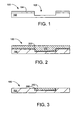
- a first substrate 102 is provided with a heater cavity etch mask 104 thereon, which is used to form a heater cavity 106 therein.
- the first substrate 102 may be a silicon wafer in which a large number of heater cavities, such as the heater cavity 106, are formed to allow making a large number of liquid metal switch devices at one time using semiconductor-type processing and multiple wafers.
- horizontal as used herein is defined as a plane parallel to a substrate or wafer.
- vertical refers to a direction perpendicular to the horizontal as just defined. Terms, such as “on”, “above”, “below”, “bottom”, “top”, “side” (as in “sidewall”), “higher”, “lower”, “over”, and “under”, are defined with respect to the horizontal plane.
- processing as used herein includes deposition of material or photoresist, patterning, exposure, development, etching, cleaning, and/or removal of the material or photoresist as required in forming a described structure.
- forming as used herein includes processes such as depositing, growing, building, chemically combining, or other processes for forming layers, films, and structures.
- the first substrate 102 may be of silicon (Si), and the barrier layer 200 may be of silicon oxide (SiO 2 ), other oxides or nitrides, e.g., silicon nitride could be used. Also, other materials may be used, and in fact, may enhance the performance, e.g. gold (provided there is additionally a sealing layer to prevent gold-mercury interaction), platinum (which will need a seed layer, such as chrome or nickel chromium), chrome, silver, nickel, or titanium.
- SiO 2 silicon oxide
- other materials may be used, and in fact, may enhance the performance, e.g. gold (provided there is additionally a sealing layer to prevent gold-mercury interaction), platinum (which will need a seed layer, such as chrome or nickel chromium), chrome, silver, nickel, or titanium.
- the sacrificial layer 202 can be any material that can be removed by an etching process that does not negatively affect the heater and other elements after construction. Two examples would be PSG (phospho-silicate glass) or aluminum, if a hydrofluoric acid wet etch is acceptable.
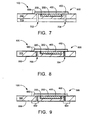
- FIG. 10 therein is shown the structure of FIG. 9 after processing of the via metalization 900 to form the pad/vias 1000 and 1002 and removal of the via masks 902 and 904.
- the pad/vias 1000 and 1002 provide the electrical connections to the heater layer 402.
- Sub-channels 1330 and 1332 are connected to the main channel 1320 between the electrodes 1322 and 1324 and between the electrodes 1324 and 1326, respectively.
- the sub-channels 1330 and 1332 also respectively connect to chambers 106 and 108 of heater units 1210 and 1212.
- Different elements of the present invention such as the channels, chambers, recesses, electrodes, seals, and heater elements, can be on different substrates and still provide an operational device.
- the first substrate 102 has the main channel 1320 filled with a liquid metal 1342, such as mercury (Hg), and a fluid non-conductor 1343, such as argon (Ar), nitrogen (N), or air.
- a liquid metal 1342 such as mercury (Hg)
- a fluid non-conductor 1343 such as argon (Ar), nitrogen (N), or air.
- the second substrate 1100 overlays the first substrate 102, and the liquid metal 1342 and the fluid non-conductor 1343 are sealed in the main channel 1320, the sub-channels 1330 and 1332, and the chambers 106 and 108 by the adhesive seals 1004.
- the fluid non-conductor 1343 is capable of being expanded by the heater elements 500 and 502 to cause divisions in the liquid metal 1342.
- the materials of the first and second substrates 102 and 1100 and of the adhesive seals 1004 are selected to avoid chemical reaction with and wetting by the liquid metal 1342. Chemical reactions may render the liquid metal 1342 incapable of conducting current or may compromise hermeticity of the seals, and wetting may make proper switching movement of the liquid metal 1342 impossible; i.e., an OFF state may not be achievable because the electrical path between the electrodes 1322, 1324, and 1326 cannot be interrupted.
- the sub-channels 1330 and 1332, the chambers 106 and 108, and portions of the main channel 1320 are filled with the fluid non-conductor 1343.
- the fluid non-conductor 1343 is capable of separating the liquid metal 1342 into discrete portions. The process will either connect the electrodes 1322 and 1324 or the electrodes 1324 and 1326 depending on whether the heater element 502 or the heater element 500 is respectively actuated.
- the method 1400 includes: providing substrates collectively having defined therein a liquid metal switch and a sub-channel connected to the liquid metal switch in a block 1402; forming in a first one of the substrates a cavity filled with sacrificial material and connected to the sub-channel in a block 1404; forming a heater element at least in part over the sacrificial material in a block 1406; forming conductive vias extending through one of the substrates to the heater element in a block 1408; removing the sacrificial material in a block 1410; and joining the substrates with an adhesive seal in a block 1412.
- the sequence of the method 1400 is not critical.
- the forming of the vias in block 1408 may be performed after removing the sacrificial material in block 1410.
Landscapes
- Engineering & Computer Science (AREA)
- Manufacturing & Machinery (AREA)
- Microelectronics & Electronic Packaging (AREA)
- Physics & Mathematics (AREA)
- Fluid Mechanics (AREA)
- Micromachines (AREA)
- Manufacture Of Switches (AREA)
Abstract
Description
Claims (10)
- A method for manufacturing a switch device comprising:providing substrates (102, 1100) collectively having defined therein a liquid metal switch (1320,1322,1324,1342) and a sub-channel (1330) connected to the liquid metal switch (1320,1322,1324,1342);forming in a first one of the substrates (102, 1100) a cavity (106) filled with sacrificial material (202) and connected to the sub-channel (1330);forming a heater element (500) at least in part over the sacrificial material (202);forming conductive vias (702, 704) extending through one of the substrates (102, 1100) to the heater element (500);removing the sacrificial material (202); andjoining the substrates (102, 1100) with an adhesive seal (1004).
- The method of claim 1 additionally comprising:forming a barrier layer (200) in the cavity (106) and on a surface of the first one of the substrates (102, 1100); andremoving the barrier layer (200) from the surface of the first one of the substrates (102, 1100).
- The method of claim 1 wherein:forming the cavity (106) comprises depositing sacrificial material (202) over the first one of the substrates (102, 1100); andplanarizing the sacrificial material (202) to be co-planar with the surface of the first one of the substrates (102, 1100).
- The method as claimed in claim 1 wherein forming the heater element (500) comprises:depositing a seed layer (200) over the sacrificial material (202);depositing a heater material layer (402) on the seed layer (200); anddefining the heater element (500) in the seed layer (200) and the heater material layer (402).
- The method as claimed in claim 1 additionally comprising:depositing passivation material (400) prior to forming the heater element (500).
- A switch device comprising:substrates (102, 1100) collectively having defined therein a liquid metal switch (1320,1322,1324,1342), a cavity (106) and a sub-channel (1330) extending between the cavity (106) and the liquid metal switch (1320,1322,1324,1342);a heater element (500) spaced from the substrates (102, 1100) in the cavity (106), the heater element (500) comprising a refractory nitride, tungsten silicon nitride, tantalum nitride, platinum, or a combination thereof;conductive vias (702, 704) electrically connected to the heater element (500); andan adhesive seal (1004) joining the substrates (102, 1100).
- The device as claimed in claim 6 additionally comprising:a barrier layer (200) comprising silicon nitride, aluminum nitride, titanium nitride, aluminum, nickel chromium, chrome, platinum, silver, gold, nickel, titanium, or a combination thereof in the cavity (106).
- The device as claimed in claim 6 wherein:the heater element (500) comprises:a seed layer (200) comprising silicon nitride, titanium nitride, aluminum nitride, chrome, nickel chrome, or a combination thereof; andheater material layer (402) on the seed layer (200); andthe heater element (500) is defined in the seed layer (200) and the heater material layer (402).
- The device as claimed in claim 6 additionally comprising:passivation material (400) comprising titanium nitride, aluminum nitride, silicon nitride, silicon dioxide, platinum or a combination thereof between the heater element (500) and one of the substrates (102, 1100).
- The device as claimed in claim 6 additionally comprising:passivation material (400) comprising titanium nitride, aluminum nitride, silicon nitride, silicon dioxide, platinum or a combination thereof over the heater element (500).
Applications Claiming Priority (2)
| Application Number | Priority Date | Filing Date | Title |
|---|---|---|---|
| US826248 | 2004-04-16 | ||
| US10/826,248 US6822176B1 (en) | 2004-04-16 | 2004-04-16 | Liquid metal switch and method of manufacture therefor |
Publications (2)
| Publication Number | Publication Date |
|---|---|
| EP1587119A2 true EP1587119A2 (en) | 2005-10-19 |
| EP1587119A3 EP1587119A3 (en) | 2005-12-21 |
Family
ID=33435678
Family Applications (1)
| Application Number | Title | Priority Date | Filing Date |
|---|---|---|---|
| EP04027442A Withdrawn EP1587119A3 (en) | 2004-04-16 | 2004-11-18 | Liquid metal switch and method of manufacture therefor |
Country Status (3)
| Country | Link |
|---|---|
| US (1) | US6822176B1 (en) |
| EP (1) | EP1587119A3 (en) |
| JP (1) | JP2005310773A (en) |
Families Citing this family (9)
| Publication number | Priority date | Publication date | Assignee | Title |
|---|---|---|---|---|
| JP2004199887A (en) * | 2002-12-16 | 2004-07-15 | Agilent Technol Inc | Electrical contact switching device using conductive fluid and method of manufacturing the same |
| JP2004227858A (en) * | 2003-01-21 | 2004-08-12 | Agilent Technol Inc | Electric contact switchgear and method for manufacturing electric contact switchgear |
| US7071432B2 (en) * | 2003-04-14 | 2006-07-04 | Agilent Technologies, Inc. | Reduction of oxides in a fluid-based switch |
| US6924443B2 (en) * | 2003-04-14 | 2005-08-02 | Agilent Technologies, Inc. | Reducing oxides on a switching fluid in a fluid-based switch |
| US7019236B2 (en) * | 2004-03-11 | 2006-03-28 | Agilent Technologies, Inc. | Switch with lid |
| US7358452B2 (en) * | 2005-06-30 | 2008-04-15 | Agilent Technlolgies, Inc. | Architecture and method of fabrication for a liquid metal microswitch (LIMMS) |
| US7211754B2 (en) * | 2005-08-01 | 2007-05-01 | Avago Technologies Ecbu Ip (Singapore) Pte. Ltd. | Fluid-based switch, and method of making same |
| ES2637381T3 (en) * | 2007-10-31 | 2017-10-13 | F. Hoffmann-La Roche Ag | Electrical standards for biosensors and manufacturing procedure |
| JP2009117078A (en) * | 2007-11-02 | 2009-05-28 | Yokogawa Electric Corp | relay |
Family Cites Families (10)
| Publication number | Priority date | Publication date | Assignee | Title |
|---|---|---|---|---|
| US6323447B1 (en) * | 1998-12-30 | 2001-11-27 | Agilent Technologies, Inc. | Electrical contact breaker switch, integrated electrical contact breaker switch, and electrical contact switching method |
| JP4183817B2 (en) * | 1998-12-30 | 2008-11-19 | アジレント・テクノロジーズ・インク | Electrical contact switchgear |
| JP2001185017A (en) * | 1999-12-22 | 2001-07-06 | Agilent Technol Inc | Switch device |
| US6689976B1 (en) * | 2002-10-08 | 2004-02-10 | Agilent Technologies, Inc. | Electrically isolated liquid metal micro-switches for integrally shielded microcircuits |
| US6457815B1 (en) | 2001-01-29 | 2002-10-01 | Hewlett-Packard Company | Fluid-jet printhead and method of fabricating a fluid-jet printhead |
| US6720507B2 (en) * | 2002-06-14 | 2004-04-13 | Agilent Technologies, Inc. | Multi-seal fluid conductor electrical switch device |
| US20040007449A1 (en) * | 2002-07-10 | 2004-01-15 | Dove Lewis R. | Add-on, suspended heater for liquid metal micro-switch |
| US6559420B1 (en) * | 2002-07-10 | 2003-05-06 | Agilent Technologies, Inc. | Micro-switch heater with varying gas sub-channel cross-section |
| JP2004074514A (en) * | 2002-08-14 | 2004-03-11 | Seiko Epson Corp | Wiping member, liquid ejecting device, ink jet recording device |
| US6743991B1 (en) * | 2003-04-14 | 2004-06-01 | Agilent Technologies, Inc. | Polymeric liquid metal switch |
-
2004
- 2004-04-16 US US10/826,248 patent/US6822176B1/en not_active Expired - Fee Related
- 2004-11-18 EP EP04027442A patent/EP1587119A3/en not_active Withdrawn
-
2005
- 2005-04-13 JP JP2005115442A patent/JP2005310773A/en active Pending
Also Published As
| Publication number | Publication date |
|---|---|
| EP1587119A3 (en) | 2005-12-21 |
| JP2005310773A (en) | 2005-11-04 |
| US6822176B1 (en) | 2004-11-23 |
Similar Documents
| Publication | Publication Date | Title |
|---|---|---|
| TW564448B (en) | Monolithic single pole double throw RF MEMS switch | |
| JP3989860B2 (en) | Semiconductor microelectromechanical (MEM) switch | |
| US6559420B1 (en) | Micro-switch heater with varying gas sub-channel cross-section | |
| US7675162B2 (en) | Interconnect structure using through wafer vias and method of fabrication | |
| JP4489651B2 (en) | Semiconductor device and manufacturing method thereof | |
| KR100766028B1 (en) | Light Emitting Diode Package And Process Of Making The Same | |
| US6822176B1 (en) | Liquid metal switch and method of manufacture therefor | |
| US20090115565A1 (en) | Liquid metal relay | |
| TW200406015A (en) | Electrically isolated liquid metal micro-switches for integrally shielded microcircuits | |
| US6806431B2 (en) | Liquid metal micro-relay with suspended heaters and multilayer wiring | |
| US6734513B2 (en) | Semiconductor device and microrelay | |
| KR101272359B1 (en) | Switch and method of manufacture thereof and relay | |
| JP4701136B2 (en) | Fluid switch and manufacturing method thereof | |
| KR20080097023A (en) | RF MEMS switch and its manufacturing method | |
| JP2004200151A (en) | Contact switch and device with contact switch | |
| CN109037175A (en) | power device and its packaging method | |
| KR100618343B1 (en) | A manufacturing method of a packaging substrate and a packaging method using the same. | |
| EP1391903B1 (en) | Micro-relay device | |
| US6872903B2 (en) | Surface joined multi-substrate liquid metal switching device | |
| US6927350B2 (en) | Multi-substrate liquid metal high-frequency switching device | |
| CN1708821A (en) | Micromechanical relays with inorganic insulation | |
| US6765162B2 (en) | Multi-seal fluid conductor electrical switch device and method of manufacture therefor | |
| EP1589553B1 (en) | A method and apparatus for producing a liquid metal switch device. | |
| US7137412B2 (en) | Relay | |
| US7358452B2 (en) | Architecture and method of fabrication for a liquid metal microswitch (LIMMS) |
Legal Events
| Date | Code | Title | Description |
|---|---|---|---|
| PUAI | Public reference made under article 153(3) epc to a published international application that has entered the european phase |
Free format text: ORIGINAL CODE: 0009012 |
|
| AK | Designated contracting states |
Kind code of ref document: A2 Designated state(s): AT BE BG CH CY CZ DE DK EE ES FI FR GB GR HU IE IS IT LI LU MC NL PL PT RO SE SI SK TR |
|
| AX | Request for extension of the european patent |
Extension state: AL HR LT LV MK YU |
|
| PUAL | Search report despatched |
Free format text: ORIGINAL CODE: 0009013 |
|
| AK | Designated contracting states |
Kind code of ref document: A3 Designated state(s): AT BE BG CH CY CZ DE DK EE ES FI FR GB GR HU IE IS IT LI LU MC NL PL PT RO SE SI SK TR |
|
| AX | Request for extension of the european patent |
Extension state: AL HR LT LV MK YU |
|
| 17P | Request for examination filed |
Effective date: 20060421 |
|
| AKX | Designation fees paid |
Designated state(s): DE FR GB |
|
| RAP1 | Party data changed (applicant data changed or rights of an application transferred) |
Owner name: AGILENT TECHNOLOGIES, INC. |
|
| STAA | Information on the status of an ep patent application or granted ep patent |
Free format text: STATUS: THE APPLICATION IS DEEMED TO BE WITHDRAWN |
|
| 18D | Application deemed to be withdrawn |
Effective date: 20090603 |