EP1583393B1 - Method and system for data logging in a listening device - Google Patents
Method and system for data logging in a listening device Download PDFInfo
- Publication number
- EP1583393B1 EP1583393B1 EP05006950.9A EP05006950A EP1583393B1 EP 1583393 B1 EP1583393 B1 EP 1583393B1 EP 05006950 A EP05006950 A EP 05006950A EP 1583393 B1 EP1583393 B1 EP 1583393B1
- Authority
- EP
- European Patent Office
- Prior art keywords
- voltage
- memory
- dsp
- entity
- level
- Prior art date
- Legal status (The legal status is an assumption and is not a legal conclusion. Google has not performed a legal analysis and makes no representation as to the accuracy of the status listed.)
- Expired - Lifetime
Links
Images

Classifications
-
- H—ELECTRICITY
- H04—ELECTRIC COMMUNICATION TECHNIQUE
- H04R—LOUDSPEAKERS, MICROPHONES, GRAMOPHONE PICK-UPS OR LIKE ACOUSTIC ELECTROMECHANICAL TRANSDUCERS; ELECTRIC HEARING AIDS; PUBLIC ADDRESS SYSTEMS
- H04R25/00—Electric hearing aids
- H04R25/30—Monitoring or testing of hearing aids, e.g. functioning, settings, battery power
- H04R25/305—Self-monitoring or self-testing
-
- H—ELECTRICITY
- H04—ELECTRIC COMMUNICATION TECHNIQUE
- H04R—LOUDSPEAKERS, MICROPHONES, GRAMOPHONE PICK-UPS OR LIKE ACOUSTIC ELECTROMECHANICAL TRANSDUCERS; ELECTRIC HEARING AIDS; PUBLIC ADDRESS SYSTEMS
- H04R2225/00—Details of deaf aids covered by H04R25/00, not provided for in any of its subgroups
- H04R2225/39—Aspects relating to automatic logging of sound environment parameters and the performance of the hearing aid during use, e.g. histogram logging, or of user selected programs or settings in the hearing aid, e.g. usage logging
-
- H—ELECTRICITY
- H04—ELECTRIC COMMUNICATION TECHNIQUE
- H04R—LOUDSPEAKERS, MICROPHONES, GRAMOPHONE PICK-UPS OR LIKE ACOUSTIC ELECTROMECHANICAL TRANSDUCERS; ELECTRIC HEARING AIDS; PUBLIC ADDRESS SYSTEMS
- H04R2460/00—Details of hearing devices, i.e. of ear- or headphones covered by H04R1/10 or H04R5/033 but not provided for in any of their subgroups, or of hearing aids covered by H04R25/00 but not provided for in any of its subgroups
- H04R2460/03—Aspects of the reduction of energy consumption in hearing devices
Definitions
- This invention relates to signal processing technology, and more particularly, to a method and system for data logging in a listening device.
- US 6 236 731 B1 discloses the features of the preamble of claim 1.
- Digital hearing aids have been developed in recent years. For example, in digital hearing aids for "In-The-Ear” (ITE) and “Behind-The-Ear” (BTE) applications, an audio signal is processed according to some processing scheme and subsequently transmitted to the user of the hearing aid through a hearing aid loud speaker (i.e. a hearing aid receiver).
- ITE In-The-Ear
- BTE Behind-The-Ear
- information such as parameters related to input and output signals or other signals may be stored in non-volatile memory during normal hearing aid operation.
- Such storing is known as data logging.
- the present invention is now described for a hearing aid.
- the present invention may be applied to different devices, such as, but not limited to, listening devices (e.g., headsets), or devices having a digital signal processor (DSP) entity and a non-volatile (NV) memory.
- listening devices e.g., headsets
- DSP digital signal processor
- NV non-volatile
- data logging is defined as the process of monitoring data (such as, but not limited to, parameters related to input and output signals or other signals like operating time) and storing data associated with the data into a NV memory.
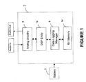
- FIG. 1 shows one example of a hearing aid system 2 to which a data logging manager 8 in accordance with an embodiment of the present invention is suitably applied.
- the hearing aid system 2 includes one or more digital signal processors (DSPs) or other audio processing entities (e.g., DSP entities).
- DSPs digital signal processors
- the hearing aid system 2 further includes analog circuitry 6 for analog signal processing, a data logging manager 8 and a NV memory 14.
- the DSP entity 12 and NV memory 14 communicate with each other.
- the DSP entity 12 executes real time processing including audio processing.
- the NV memory 14 is used to store logged data as described below.
- the data logging manager 8 manages data logging process during a normal hearing aid operation. Data are transferred between the NV memory 14 and the DSP entity 12 through the data logging manager 8.
- the data logging manager 8 may be automatically or manually enabled and disabled by the DSP entity 12.
- the NV memory 14 may also be used for storage of application code and information relevant to a specific application, such as fitting information.
- the application code represents signal processing algorithms and other system processing, and is the code that the DSP entity 12 executes during operation.
- the fitting information is used to configure the algorithm in order to provide the signal enhancement for a specific hearing impaired user or range of users. In most cases, the fitting information is different for each user, and is stored on a per-user basis, but this is not a requirement.
- the information relevant to a specific application may include manufacturing information related to tracking the origin of a given hearing aid system in case of the return of a defect part.
- the NV memory 14 may include an EEPROM, flash memory, other similar NV memory, such as storage elements/modules/memories for storing data in non-volatile manner, or combinations thereof.
- the data logging manager 8 is provided separately from the DSP entity 12 and the NV memory 14. However, the data logging manager 8 may be incorporated into the DSP entity, the NV memory 14 or a combination thereof.
- the analog circuitry 6, the DSP entity 12 and the data logging manager 8 may be comprised of one or several interconnected integrated circuits that form a circuitry.
- a battery 1 supplies power to the hearing aid system 2.
- the battery 1 is shown as separated from the hearing aid system 2. However, the battery 1 may be provided within the hearing aid system 2.
- the data logging manager 8 may includes a level translating element or module (30) for level translation between the DSP entity 12 and the NV memory 14 as described below.
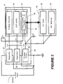
- FIG. 2 shows a detailed example of the hearing aid system 2 for data logging.
- the hearing aid system 2 of Figure 2 includes a subsystem 10 and a NV storage module 20.
- "16" corresponds to the DSP entity 12 in Figure 1
- "24" corresponds to the NV memory 14 in Figure 1 .
- the subsystem 10 contains a DSP entity 16, in which the signal processing is performed, and one or more input/output (I/O) pads 18.
- the I/O pads 18 incorporate the level translating element 30.
- the subsystem 10 may be an integrated circuit or several interconnected integrated circuits forming a circuitry.
- the NV storage module 20 includes a NV memory 24 and one or more I/O pads 22.
- the DSP entity 16 and the NV memory 24 communicate with each other through the I/O pads 18 and the I/O pads 22.
- the NV memory 24 is provided separately from the subsystem 10. However, the NV memory 24 may also be embedded in the subsystem 10.
- the level translating element 30 performs level translation to communication signals transmitted between the DSP entity 16 and the NV memory 24.
- the level translating element 30 allows communication signals from the DSP entity 16 to be voltage-translated to the voltage at which the NV storage module 20 requires for communication.
- the level translating element 30 allows signals from the NV storage module 20 to be voltage-translated to the same voltage at which the DSP entity 16 required for communication.
- the level translation may be automatically reenabled under automatic or manual control of the DSP entity 16 whenever data logging is needed.
- level translating element 30 is contained within the NV storage module 20, such as I/O pads 22, is also possible and that this configuration is functionally equivalent to the configuration described above.
- the level translating element 30 utilizes voltages generated by a set of voltage generators, such as charge pumps, regulators, or similar units for converting voltage from the battery 1 into a plurality of operating voltages.
- a set of voltage generators such as charge pumps, regulators, or similar units for converting voltage from the battery 1 into a plurality of operating voltages.
- voltage regulators 26 and 27, and a charge pump 28 are provided for converting voltage.
- the voltage regulators 26 and 27 are connected to the battery 1.
- the voltage regulator 26 provides a regulated voltage V1 to the DSP entity 16 and to the level translating element 30.
- the voltage regulator 27 provides a regulated voltage VA to the analog circuitry 6.
- the charge pump 28 boosts the regulated voltage VA to a voltage V2, which is sufficiently high to operate the NV storage module 20, and provides the voltage V2 to the level translating element 30 and the NV storage module 20.
- the regulated voltage V1 is filtered by a filtering capacitor C1.
- the filtering capacitor C1 is provided to the V1 to obtain a low-noise voltage at node N1, to which the DSP entity 16 and the level translating element 30 are connected.
- the voltage V2 is filtered by a filtering capacitor C2.
- the filtering capacitor C2 is provided to the V2 to obtain a low-noise voltage at node N2, to which the level translating element 30 and the NV storage module 20 are connected.
- the level translating element 30 has two ports; a first port and a second port.
- the first port communicates with the DSP entity 16 via bi-directional communication signals that are level translated as described above.
- the second port communicates with the I/O pad 22 via bi-directional communication signals that are level translated as described above.
- the V1 voltage at node N1 is supplied to the first port in the level translating element 30.
- the V2 voltage at node N2 is supplied to the second port in the level translating element 30.
- the level translating element 30 translates a signal (P1) with the voltage V1, which is provided on the first port, to the same signal (P1) with the voltage V2, which is provided on the second port.
- the signal (P1) with the voltage V2 is then provided to the I/O pads 22.
- the level translating element 30 translates a signal (P2) with the voltage V2, which is provided on the second port, to the same signal (P2) with the voltage V1, which is provided on the first port.
- the signal (P2) with the voltage V1 is then provided to the DSP entity 16.
- the level translating element 30 may have a circuitry or a number of interconnected circuitries.
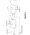
- FIG 3 shows one example of the level translating element 30 of Figure 2 .
- “40" represents the first port which communicates with the DSP entity 16
- "42" represents a second port which communicates with the I/O pad 22.
- the level translating element 30 may include two circuitries 44 and 46.
- the circuitry 44 is embedded in the first port 40 that operates at the low voltage V1.
- the circuitry 46 is embedded in the second port 42 that operates at the higher voltage V2.
- the circuitries 44 and 46 are interconnected to each other. Each circuitry is enabled during data logging for voltage level translation.
- the interconnected circuitries 44 and 46 convert a signal S1 with an input voltage V1 to a signal S2 with an output voltage V2.
- the interconnected circuitries 44 and 46 convert a signal S2 with an input voltage V2 to a signal S1 with an output voltage V1.
- the methodology described above only performs voltage conversion of signals delivered to the I/O pads 18.
- the level translating element 30 may be implemented outside the actual I/O pad (leaving the pad to constitute a connection between the DSP entity 16 and the I/O pad 22 in the NV storage module 20 only).
- An alternative way of logging data would be to perform switching of operating voltage whenever data logging is required.
- the voltage of the node N1 is switched from the V1 voltage to the voltage V2.
- the voltage switching allows the DSP entity 16 and the NV storage module 20 to communicate with each other at the same voltage V2.
- this approach requires the whole subsystem (entity) 10 including I/O pads 18 to operate at the voltage V2.
- Operating the whole entity 10 on the voltage V2 causes undesirable audio artifacts.
- the filtering capacitor C1 would need additional charge to change the V1 voltage to the V2 voltage. This will cause the charge pump voltage to drop, and will cause audible side effects on the signal chain in the analog circuitry 6, since the charge pump voltage is generated from the VA.
- the VA is a voltage sensitive to variations since it supplies the noise-critical analog circuitry 6.
- the level translating element 30 operates on the voltage V2.
- the subsystem 10 does not require any transfer of charge between the filtering capacitors C1 and C2 to access the NV storage module 20 since no switching of operating voltages are performed. Thus, no audible side effects are present during data logging when performing the voltage level translation.
- More circuitry operates at a higher operating voltage when the voltage switching is employed for data logging, as compared to the level translation. Further, it is well known to a person skilled in the art that power consumed is proportional to the square of operating voltage. Thus, the voltage level translation also results in less power consumption than that of the switching.
- examples 1)-2) of use for a data logging application are described below. It is noted that the use of a data logging application is not limited to any of these examples 1)-2).
- information related to an incoming signal or other part of the signal chain, or other statistics may be provided from the DSP entity (e.g., 12 of Figure 1 , 16 of Figure 2 ) or other part of the signal chain, and is stored in the NV memory (e.g., 14 of Figure 1 , 24 of Figure 2 ).
- the DSP entity can perform signal processing including data logging without interrupting or corrupting the overall audio quality of the audio signal.
- parameters representing a surrounding sound environment may be extracted from an input signal as part of the signal processing in the DSP entity. These parameters are stored in the NV memory at discrete time intervals during normal hearing aid audio processing as shown in Figure 4 .
- Figure 4 is a flow chart showing one example of a system operation for the hearing aid system 2 of Figure 2 .
- step S2 when the hearing aid system 2 is turned on (step S2), the hearing aid system 2, under automatic or manual control of the DSP entity 16, enables the level translation mode (step S4).
- the level translating element 30 is turned on.
- Data logging is started (step S6).
- the DSP entity 16 stores data to be logged in the NV memory 24. After waiting a pre-determined or random time, it is determined whether there are any data to be logged (step S8). If the hearing aid system 2 does not need any more data to be logged, then the level translation mode is turned off (step S10). If yes, the system goes to step S6
- the level translation is performed to the communication signals, which are related to data-logging and are transferred between a DSP entity and a storage element or module.
- the logged data is stored in a non-volatile (NV) manner. This prevents audible side effects associated with data logging, i.e. read/write to and from the NV memory and the DSP entity, and also reduces the power consumed during data logging.
- NV non-volatile
- logged data such as information/parameters
- NV memory during a normal hearing aid operation. This prevents the logged parameters from being erased upon power down or reset of the hearing aid system.
- the data logging manager of the present invention may be implemented by any hardware, software or a combination of hardware and software having the above described functions.
- the software code either in its entirety or a part thereof, may be stored in a computer readable medium.
- a computer data signal representing the software code which may be embedded in a carrier wave may be transmitted via a communication network.
- Such a computer readable medium and, a computer data signal and carrier wave are also within the scope of the present invention, as well as the hardware, software and the combination thereof.
Landscapes
- Health & Medical Sciences (AREA)
- General Health & Medical Sciences (AREA)
- Otolaryngology (AREA)
- Neurosurgery (AREA)
- Physics & Mathematics (AREA)
- Engineering & Computer Science (AREA)
- Acoustics & Sound (AREA)
- Signal Processing (AREA)
- Measurement Of Current Or Voltage (AREA)
- Debugging And Monitoring (AREA)
Description
- This invention relates to signal processing technology, and more particularly, to a method and system for data logging in a listening device.
US 6 236 731 B1 discloses the features of the preamble ofclaim 1. - Digital hearing aids have been developed in recent years. For example, in digital hearing aids for "In-The-Ear" (ITE) and "Behind-The-Ear" (BTE) applications, an audio signal is processed according to some processing scheme and subsequently transmitted to the user of the hearing aid through a hearing aid loud speaker (i.e. a hearing aid receiver).
- For the signal processing, information such as parameters related to input and output signals or other signals may be stored in non-volatile memory during normal hearing aid operation. Such storing is known as data logging.
- Because of current consumption limitations and audio artifacts that can be inadvertently caused, currently available hearing aids cannot perform data logging during the normal hearing aid operation (i.e., when the hearing aid is reproducing audio) without audible side-effects and excessive current drain.
- Therefore, there is a need for providing a new method and system, which can execute data logging during normal hearing aid operation without audible side-effects and also provide reduced current drain.
- It is an object of the invention to provide a novel method and system that obviates or mitigates at least one of the disadvantages of existing systems. The apparatus and method of the present invention are defined in the independent claims.
- Other aspects and features of the present invention will be readily apparent to those skilled in the art from a review of the following detailed description of preferred embodiments in conjunction with the accompanying drawings.
- This summary of the invention does not necessarily describe all features of the invention.
- These and other features of the invention will become more apparent from the following description in which reference is made to the appended drawings wherein:
-
Figure 1 is a block diagram showing one example of a hearing aid system to which a data logging manager in accordance with an embodiment of the present invention is suitably applied; -
Figure 2 is a schematic diagram showing a detailed example of the hearing aid system ofFigure 1 ; -
Figure 3 is a schematic diagram showing an example of the level translating element ofFigure 2 ; and -
Figure 4 is a flow chart showing one example of a system operation for the hearing aid system ofFigure 2 . - The embodiment of the present invention is now described for a hearing aid. However, the present invention may be applied to different devices, such as, but not limited to, listening devices (e.g., headsets), or devices having a digital signal processor (DSP) entity and a non-volatile (NV) memory.
- In the embodiment of the present invention, data logging is defined as the process of monitoring data (such as, but not limited to, parameters related to input and output signals or other signals like operating time) and storing data associated with the data into a NV memory.
-
Figure 1 shows one example of ahearing aid system 2 to which adata logging manager 8 in accordance with an embodiment of the present invention is suitably applied. Thehearing aid system 2 includes one or more digital signal processors (DSPs) or other audio processing entities (e.g., DSP entities). InFigure 1 , oneDSP entity 12 is shown. Thehearing aid system 2 further includesanalog circuitry 6 for analog signal processing, adata logging manager 8 and aNV memory 14. - The
DSP entity 12 andNV memory 14 communicate with each other. TheDSP entity 12 executes real time processing including audio processing. TheNV memory 14 is used to store logged data as described below. Thedata logging manager 8 manages data logging process during a normal hearing aid operation. Data are transferred between theNV memory 14 and theDSP entity 12 through thedata logging manager 8. Thedata logging manager 8 may be automatically or manually enabled and disabled by theDSP entity 12. - The
NV memory 14 may also be used for storage of application code and information relevant to a specific application, such as fitting information. The application code represents signal processing algorithms and other system processing, and is the code that theDSP entity 12 executes during operation. The fitting information is used to configure the algorithm in order to provide the signal enhancement for a specific hearing impaired user or range of users. In most cases, the fitting information is different for each user, and is stored on a per-user basis, but this is not a requirement. The information relevant to a specific application may include manufacturing information related to tracking the origin of a given hearing aid system in case of the return of a defect part. - The
NV memory 14 may include an EEPROM, flash memory, other similar NV memory, such as storage elements/modules/memories for storing data in non-volatile manner, or combinations thereof. - In
Figure 1 , thedata logging manager 8 is provided separately from theDSP entity 12 and theNV memory 14. However, thedata logging manager 8 may be incorporated into the DSP entity, theNV memory 14 or a combination thereof. Theanalog circuitry 6, theDSP entity 12 and thedata logging manager 8 may be comprised of one or several interconnected integrated circuits that form a circuitry. - A
battery 1 supplies power to thehearing aid system 2. InFigure 1 , thebattery 1 is shown as separated from thehearing aid system 2. However, thebattery 1 may be provided within thehearing aid system 2. - The
data logging manager 8 may includes a level translating element or module (30) for level translation between theDSP entity 12 and theNV memory 14 as described below. -
Figure 2 shows a detailed example of thehearing aid system 2 for data logging. Thehearing aid system 2 ofFigure 2 includes asubsystem 10 and aNV storage module 20. InFigure 2 , "16" corresponds to theDSP entity 12 inFigure 1 , and "24" corresponds to theNV memory 14 inFigure 1 . - The
subsystem 10 contains aDSP entity 16, in which the signal processing is performed, and one or more input/output (I/O)pads 18. The I/O pads 18 incorporate thelevel translating element 30. Thesubsystem 10 may be an integrated circuit or several interconnected integrated circuits forming a circuitry. - The
NV storage module 20 includes aNV memory 24 and one or more I/O pads 22. TheDSP entity 16 and theNV memory 24 communicate with each other through the I/O pads 18 and the I/O pads 22. InFigure 2 , theNV memory 24 is provided separately from thesubsystem 10. However, theNV memory 24 may also be embedded in thesubsystem 10. - The
level translating element 30 performs level translation to communication signals transmitted between theDSP entity 16 and theNV memory 24. Thelevel translating element 30 allows communication signals from theDSP entity 16 to be voltage-translated to the voltage at which theNV storage module 20 requires for communication. Similarly, thelevel translating element 30 allows signals from theNV storage module 20 to be voltage-translated to the same voltage at which theDSP entity 16 required for communication. The level translation may be automatically reenabled under automatic or manual control of theDSP entity 16 whenever data logging is needed. - It is recognized that an equivalent arrangement where the
level translating element 30 is contained within theNV storage module 20, such as I/O pads 22, is also possible and that this configuration is functionally equivalent to the configuration described above. - One example of the
level translating element 30 is now described in detail. Thelevel translating element 30 utilizes voltages generated by a set of voltage generators, such as charge pumps, regulators, or similar units for converting voltage from thebattery 1 into a plurality of operating voltages. - In
Figure 2 ,voltage regulators charge pump 28 are provided for converting voltage. Thevoltage regulators battery 1. Thevoltage regulator 26 provides a regulated voltage V1 to theDSP entity 16 and to thelevel translating element 30. Thevoltage regulator 27 provides a regulated voltage VA to theanalog circuitry 6. Thecharge pump 28 boosts the regulated voltage VA to a voltage V2, which is sufficiently high to operate theNV storage module 20, and provides the voltage V2 to thelevel translating element 30 and theNV storage module 20. - The regulated voltage V1 is filtered by a filtering capacitor C1. The filtering capacitor C1 is provided to the V1 to obtain a low-noise voltage at node N1, to which the
DSP entity 16 and thelevel translating element 30 are connected. The voltage V2 is filtered by a filtering capacitor C2. The filtering capacitor C2 is provided to the V2 to obtain a low-noise voltage at node N2, to which thelevel translating element 30 and theNV storage module 20 are connected. - In the example, the
level translating element 30 has two ports; a first port and a second port. The first port communicates with theDSP entity 16 via bi-directional communication signals that are level translated as described above. The second port communicates with the I/O pad 22 via bi-directional communication signals that are level translated as described above. The V1 voltage at node N1 is supplied to the first port in thelevel translating element 30. The V2 voltage at node N2 is supplied to the second port in thelevel translating element 30. Thelevel translating element 30 translates a signal (P1) with the voltage V1, which is provided on the first port, to the same signal (P1) with the voltage V2, which is provided on the second port. The signal (P1) with the voltage V2 is then provided to the I/O pads 22. Thelevel translating element 30 translates a signal (P2) with the voltage V2, which is provided on the second port, to the same signal (P2) with the voltage V1, which is provided on the first port. The signal (P2) with the voltage V1 is then provided to theDSP entity 16. Thelevel translating element 30 may have a circuitry or a number of interconnected circuitries. -
Figure 3 shows one example of thelevel translating element 30 ofFigure 2 . InFigure 3 , "40" represents the first port which communicates with theDSP entity 16, and "42" represents a second port which communicates with the I/O pad 22. As shown inFigure 3 , thelevel translating element 30 may include twocircuitries circuitry 44 is embedded in thefirst port 40 that operates at the low voltage V1. Thecircuitry 46 is embedded in thesecond port 42 that operates at the higher voltage V2. Thecircuitries interconnected circuitries interconnected circuitries O pads 18. - Different implementation schemes may exist. For example, the
level translating element 30 may be implemented outside the actual I/O pad (leaving the pad to constitute a connection between theDSP entity 16 and the I/O pad 22 in theNV storage module 20 only). - An alternative way of logging data would be to perform switching of operating voltage whenever data logging is required. Upon the switching, the voltage of the node N1 is switched from the V1 voltage to the voltage V2. The voltage switching allows the
DSP entity 16 and theNV storage module 20 to communicate with each other at the same voltage V2. However, this approach requires the whole subsystem (entity) 10 including I/O pads 18 to operate at the voltage V2. Operating thewhole entity 10 on the voltage V2 causes undesirable audio artifacts. In the voltage switching moment, the filtering capacitor C1 would need additional charge to change the V1 voltage to the V2 voltage. This will cause the charge pump voltage to drop, and will cause audible side effects on the signal chain in theanalog circuitry 6, since the charge pump voltage is generated from the VA. The VA is a voltage sensitive to variations since it supplies the noise-critical analog circuitry 6. - By contrast, in the embodiment of the present invention, only the
level translating element 30 operates on the voltage V2. Thesubsystem 10 does not require any transfer of charge between the filtering capacitors C1 and C2 to access theNV storage module 20 since no switching of operating voltages are performed. Thus, no audible side effects are present during data logging when performing the voltage level translation. - More circuitry operates at a higher operating voltage when the voltage switching is employed for data logging, as compared to the level translation. Further, it is well known to a person skilled in the art that power consumed is proportional to the square of operating voltage. Thus, the voltage level translation also results in less power consumption than that of the switching.
- Referring to
Figures 1 and2 , examples 1)-2) of use for a data logging application are described below. It is noted that the use of a data logging application is not limited to any of these examples 1)-2). - 1) In a data logging application, information related to an incoming signal or other part of the signal chain, or other statistics may be provided from the DSP entity (e.g., 12 of
Figure 1 , 16 ofFigure 2 ) or other part of the signal chain, and is stored in the NV memory (e.g., 14 ofFigure 1 , 24 ofFigure 2 ). Using the level translation, the DSP entity can perform signal processing including data logging without interrupting or corrupting the overall audio quality of the audio signal. - 2) In a data logging application, parameters representing a surrounding sound environment may be extracted from an input signal as part of the signal processing in the DSP entity. These parameters are stored in the NV memory at discrete time intervals during normal hearing aid audio processing as shown in
Figure 4 . -
Figure 4 is a flow chart showing one example of a system operation for thehearing aid system 2 ofFigure 2 . - Referring to
Figures 2 and4 , when thehearing aid system 2 is turned on (step S2), thehearing aid system 2, under automatic or manual control of theDSP entity 16, enables the level translation mode (step S4). Thelevel translating element 30 is turned on. Data logging is started (step S6). TheDSP entity 16 stores data to be logged in theNV memory 24. After waiting a pre-determined or random time, it is determined whether there are any data to be logged (step S8). If thehearing aid system 2 does not need any more data to be logged, then the level translation mode is turned off (step S10). If yes, the system goes to step S6 - According to the embodiment of the present invention, the level translation is performed to the communication signals, which are related to data-logging and are transferred between a DSP entity and a storage element or module. In the storage element or module, the logged data is stored in a non-volatile (NV) manner. This prevents audible side effects associated with data logging, i.e. read/write to and from the NV memory and the DSP entity, and also reduces the power consumed during data logging.
- According to the embodiment of the present invention, logged data, such as information/parameters, are stored in the NV memory during a normal hearing aid operation. This prevents the logged parameters from being erased upon power down or reset of the hearing aid system.
- The data logging manager of the present invention may be implemented by any hardware, software or a combination of hardware and software having the above described functions. The software code, either in its entirety or a part thereof, may be stored in a computer readable medium. Further, a computer data signal representing the software code which may be embedded in a carrier wave may be transmitted via a communication network. Such a computer readable medium and, a computer data signal and carrier wave are also within the scope of the present invention, as well as the hardware, software and the combination thereof.
- The present invention has been described with regard to one or more embodiments. However, it will be apparent to persons skilled in the art that a number of variations and modifications can be made without departing from the scope of the invention as defined in the claims.
Claims (17)
- A listening device (2) comprising:a digital signal processing, i.e. DSP, entity (12, 16) for performing real time system processing including audio processing, the DSP entity operating with a first voltage (V1);a non-volatile, i.e. NV, memory (14, 24) for communicating with the DSP entity and storing logged data during an operation of the listening device when it reproduces audio, the NV memory operating with a second voltage (V2) different from the first voltage (V1);characterized bya data logging manager (8, 26, 27, 30) for managing data logging to the NV memory during the reproduction of audio to prevent audible side effects associated with the data logging, the data logging manager including:a level translating module (30) connected to the first voltage (V1) and the second voltage (V2), for performing voltage level translation to communication signals including a first communication signal transferred from the DSP entity to the NV memory and a second communication signal transferred from the NV memory to the DSP entity;a first voltage regulator (26) connected to the DSP entity and the level translating module, for providing the first voltage (V1) to the DSP entity and the level translating module;a second voltage regulator (27) connected to a charge pump (28); andthe charge pump (28) connected to the level translating module (30) and the NV memory, for providing the second voltage (V2) to the level translating module and the NV memory.
- A device as claimed in claim 1, wherein the level translating module (30) includes:a first port (40) for communicating at the first voltage (V1) with the DSP entity (12, 16),a second port (42) for communicating at the second voltage (V2) with the NV memory (14, 24), anda converting module (44, 46) for converting a voltage of a communication signal on each of the first port and the second port,wherein the first communication signal provided on the first port from the DSP entity, is converted to the first communication signal with the second voltage (V2) and is provided to the second port, andwherein the second communication signal provided on the second port from the NV memory, is converted to the second communication signal with the first voltage (V1) and is provided to the first port.
- A device as claimed in claim 2, wherein the converting module includes a first circuitry (44) embedded in the first port and for being enabled at the data logging and performing voltage level conversion, and a second circuitry (46) embedded in the second port and for being enabled at the data logging and performing voltage level conversion, and wherein the first and second circuitries are interconnected to each other.
- A device as claimed in claim 3, wherein the first and second circuitries are enabled by the DSP entity (12, 16).
- A device as claimed in any one of claims 1 to 4, further comprising a subsystem which includes an audio circuitry for the audio signal processing, the DSP entity (12, 16), the NV memory (14, 24) or combinations thereof.
- A device as claimed in any one of claims 1 to 5, wherein the level translating module (30) is embedded in an input/output (I/O) pad (18) provided to the DSP entity (12, 16), an I/O pad (22) provided to the NV memory (14, 24) or a combination thereof.
- A device as claimed in claim 6, wherein the data logging manager is embedded in the DSP entity (12, 16), the NV memory (14, 24) or a combination thereof.
- A device as claimed in any one of claims 1 to 5, wherein the level translating module (30) is provided external to the DSP entity (12, 16) and the NV memory (14, 24) .
- A device as claimed in claim 8, wherein the data logging manager (8) is provided external to the DSP entity (12, 16) and the NV memory (14, 24) .
- A device as claimed in any one of claims 1 to 9, further comprising an analog circuitry (6) for performing analog signal processing, which is embedded into the same circuit as the DSP entity (12, 16).
- A device as claimed in any one of claims 1 to 10, wherein the NV memory (14, 24) includes an EEPROM, flash memory, other similar NV memory, or combinations thereof.
- A device as claimed in any one of claims 1 to 11, wherein the NV memory (14, 24) is embedded into the same circuit as the DSP entity (12, 16).
- A method of executing data logging during reproduction of audio in a listening device to prevent audible side effects associated with the data logging, the listening device comprising:a digital signal processing, i.e. DSP, entity (12, 16) for system processing including audio processing, the DSP entity operating with a first voltage (V1);a non-volatile, i.e. NV, memory (14, 24) for storing logged data, the NV memory operating with a second voltage (V2) different than the first voltage (V1);a level translating module (30) connected to the first voltage (V1) and the second voltage (V2), for performing voltage level translation to communication signals;a first voltage regulator (26) connected to the DSP entity and the level translating module, for providing the first voltage (V1) to the DSP entity and the level translating module;a second voltage regulator (27) connected to a charge pump (28); andthe charge pump (28) connected to the level translating module and the NV memory, for providing the second voltage (V2) to the level translating module and the NV memory,the method comprising the steps of:performing communication between the DSP entity and NV memory, including storing logged data at the NV memory during operation of the listening device when it reproduces audio, andmanaging data logging during the operation of the listening device, including:translating a voltage level of a first communication signal transferred from the DSP entity to the NV memory from the first voltage (V1) to the second voltage (V2); andtranslating a voltage level of a second communication signal transferred from the NV memory to the DSP entity from the second voltage (V2)to the first voltage (V1).
- A method as claimed in claim 13, wherein the translating step includes at least one of the following steps:performing voltage conversion of the first communication signal transferred from the DSP entity (12, 16) to the NV memory (14, 24); andperforming voltage conversion of the second communication signal transferred from the NV memory to the DSP entity.
- A method as claimed in claim 13, wherein the translating step includes the steps of:(a) performing a voltage level translation to the first communication signal with the first voltage (V1) from the DSP entity (12, 16) to provide the first communication signal with the second voltage (V2), and(b) performing a voltage level translation to the second communication signal with the second voltage (V2) from the NV memory (14, 24) to provide the second communication signal with the first voltage (V1).
- A method as claimed in any one of claims 13-15, further comprising the step of:enabling the voltage level translation by the DSP entity (12, 16) when turning on the listening device.
- A device as claimed in any one of claims 1 to 12, wherein the level translating module is enabled or disabled under the control of the DSP entity (12, 16).
Applications Claiming Priority (2)
| Application Number | Priority Date | Filing Date | Title |
|---|---|---|---|
| CA002462497A CA2462497A1 (en) | 2004-03-30 | 2004-03-30 | Method and system for data logging in a listening device |
| CA2462497 | 2004-03-30 |
Publications (3)
| Publication Number | Publication Date |
|---|---|
| EP1583393A2 EP1583393A2 (en) | 2005-10-05 |
| EP1583393A3 EP1583393A3 (en) | 2009-12-16 |
| EP1583393B1 true EP1583393B1 (en) | 2016-07-27 |
Family
ID=34865999
Family Applications (1)
| Application Number | Title | Priority Date | Filing Date |
|---|---|---|---|
| EP05006950.9A Expired - Lifetime EP1583393B1 (en) | 2004-03-30 | 2005-03-30 | Method and system for data logging in a listening device |
Country Status (5)
| Country | Link |
|---|---|
| US (1) | US7706902B2 (en) |
| EP (1) | EP1583393B1 (en) |
| CA (2) | CA2462497A1 (en) |
| DK (1) | DK1583393T3 (en) |
| WO (1) | WO2005096667A1 (en) |
Families Citing this family (3)
| Publication number | Priority date | Publication date | Assignee | Title |
|---|---|---|---|---|
| JP4704099B2 (en) * | 2004-05-21 | 2011-06-15 | ローム株式会社 | Power supply device and electronic device using the same |
| US9814879B2 (en) | 2013-05-13 | 2017-11-14 | Cochlear Limited | Method and system for use of hearing prosthesis for linguistic evaluation |
| US9923457B2 (en) * | 2015-04-23 | 2018-03-20 | Taiwan Semiconductor Manufacturing Company, Ltd. | Regulated power converter and method of operating the same |
Citations (2)
| Publication number | Priority date | Publication date | Assignee | Title |
|---|---|---|---|---|
| EP0114504A2 (en) * | 1982-12-29 | 1984-08-01 | Fujitsu Limited | Semiconductor memory device |
| EP0633576A2 (en) * | 1993-07-05 | 1995-01-11 | Mitsubishi Denki Kabushiki Kaisha | Semiconductor integrated circuit |
Family Cites Families (21)
| Publication number | Priority date | Publication date | Assignee | Title |
|---|---|---|---|---|
| US4731850A (en) * | 1986-06-26 | 1988-03-15 | Audimax, Inc. | Programmable digital hearing aid system |
| US4972487A (en) * | 1988-03-30 | 1990-11-20 | Diphon Development Ab | Auditory prosthesis with datalogging capability |
| US5410632A (en) * | 1991-12-23 | 1995-04-25 | Motorola, Inc. | Variable hangover time in a voice activity detector |
| US5197332A (en) * | 1992-02-19 | 1993-03-30 | Calmed Technology, Inc. | Headset hearing tester and hearing aid programmer |
| US5332928A (en) * | 1992-12-10 | 1994-07-26 | Threepenny Electronics Corporation | Battery drain reducer |
| US5742781A (en) * | 1996-08-09 | 1998-04-21 | Hitachi America, Ltd. | Decoded instruction buffer apparatus and method for reducing power consumption in a digital signal processor |
| US6259631B1 (en) * | 1996-09-13 | 2001-07-10 | Texas Instruments Incorporated | Row drive circuit equipped with feedback transistors for low voltage flash EEPROM memories |
| US6150837A (en) * | 1997-02-28 | 2000-11-21 | Actel Corporation | Enhanced field programmable gate array |
| US6236731B1 (en) * | 1997-04-16 | 2001-05-22 | Dspfactory Ltd. | Filterbank structure and method for filtering and separating an information signal into different bands, particularly for audio signal in hearing aids |
| US5896044A (en) * | 1997-12-08 | 1999-04-20 | Lucent Technologies, Inc. | Universal logic level shifting circuit and method |
| US6166960A (en) * | 1999-09-24 | 2000-12-26 | Microchip Technology, Incorporated | Method, system and apparatus for determining that a programming voltage level is sufficient for reliably programming an eeprom |
| AU768987B2 (en) * | 2000-01-07 | 2004-01-15 | Widex A/S | A digital hearing aid with a voltage converter |
| US20030112988A1 (en) | 2000-01-21 | 2003-06-19 | Graham Naylor | Method for improving the fitting of hearing aids and device for implementing the method |
| US6792582B1 (en) * | 2000-11-15 | 2004-09-14 | International Business Machines Corporation | Concurrent logical and physical construction of voltage islands for mixed supply voltage designs |
| US6904156B1 (en) * | 2001-08-03 | 2005-06-07 | Zarlink Semiconductor (U.S.) Inc. | System and method for reducing hearing aid squeal |
| DK1367857T3 (en) | 2002-05-30 | 2012-06-04 | Gn Resound As | Method of data recording in a hearing prosthesis |
| GB2389759A (en) | 2002-06-12 | 2003-12-17 | Zarlink Semiconductor Ltd | A signal processing system and method |
| US6820240B2 (en) * | 2002-09-25 | 2004-11-16 | International Business Machines Corporation | Voltage island chip implementation |
| EP1320282A3 (en) * | 2003-03-25 | 2004-01-07 | Phonak Ag | Method for recording of information in a hearing aid and such a hearing aid |
| US7075140B2 (en) * | 2003-11-26 | 2006-07-11 | Gregorio Spadea | Low voltage EEPROM memory arrays |
| US7324652B2 (en) * | 2003-12-30 | 2008-01-29 | Starkey Laboratories, Inc. | Hearing aid having a supply source providing multiple supply voltages |
-
2004
- 2004-03-30 CA CA002462497A patent/CA2462497A1/en not_active Abandoned
-
2005
- 2005-03-28 US US11/091,747 patent/US7706902B2/en not_active Expired - Lifetime
- 2005-03-29 CA CA2561878A patent/CA2561878C/en not_active Expired - Lifetime
- 2005-03-29 WO PCT/CA2005/000452 patent/WO2005096667A1/en not_active Ceased
- 2005-03-30 DK DK05006950.9T patent/DK1583393T3/en active
- 2005-03-30 EP EP05006950.9A patent/EP1583393B1/en not_active Expired - Lifetime
Patent Citations (2)
| Publication number | Priority date | Publication date | Assignee | Title |
|---|---|---|---|---|
| EP0114504A2 (en) * | 1982-12-29 | 1984-08-01 | Fujitsu Limited | Semiconductor memory device |
| EP0633576A2 (en) * | 1993-07-05 | 1995-01-11 | Mitsubishi Denki Kabushiki Kaisha | Semiconductor integrated circuit |
Also Published As
| Publication number | Publication date |
|---|---|
| US7706902B2 (en) | 2010-04-27 |
| US20050234572A1 (en) | 2005-10-20 |
| CA2462497A1 (en) | 2005-09-30 |
| DK1583393T3 (en) | 2016-11-14 |
| EP1583393A3 (en) | 2009-12-16 |
| EP1583393A2 (en) | 2005-10-05 |
| CA2561878A1 (en) | 2005-10-13 |
| CA2561878C (en) | 2011-07-12 |
| WO2005096667A1 (en) | 2005-10-13 |
Similar Documents
| Publication | Publication Date | Title |
|---|---|---|
| CN109863676A (en) | AC/DC power adapter with accessible internal memory | |
| EP4135303B1 (en) | Method for preventing missed calls, system, electronic device, and storage medium | |
| WO2021185105A1 (en) | Method for switching between sim card and esim card, and electronic device | |
| CN110742580A (en) | Sleep state identification method and device | |
| CN111145752B (en) | Intelligent audio device, method, electronic device and computer readable medium | |
| US20250080062A1 (en) | Method for Improving Sound Play Effect and Related Apparatus | |
| CN113391838A (en) | Microphone resource access method, operating system, terminal and virtual microphone | |
| US7706902B2 (en) | Method and system for data logging in a listening device | |
| US7552245B2 (en) | Communication card with three operational states | |
| CN113438643B (en) | Terminal capability reporting system, method, electronic equipment and storage medium | |
| US10993045B1 (en) | Hearing devices and methods for implementing automatic sensor-based on/off control of a hearing device | |
| US20200100038A1 (en) | Method of operating a hearing aid fitting system and a hearing aid fitting system | |
| CN117130975B (en) | Bus interface expansion method and related equipment | |
| CN110430105A (en) | Smart machine control method, system, computer equipment and readable storage medium storing program for executing | |
| EP2866471B1 (en) | Hearing instrument with interruptable microphone power supply | |
| US20050272416A1 (en) | Personalization of accessories coupled to a communications device | |
| CN114945176A (en) | Clipboard access control method, electronic device and storage medium | |
| KR100664138B1 (en) | External speaker device using SD card slot | |
| EP3530008A1 (en) | Wireless hearing device comprising split pairing tables | |
| CN117130959B (en) | Bus control method, electronic device and computer storage medium | |
| CN111797432A (en) | Convenient human health data sharing system based on Internet of things | |
| CN114786117B (en) | A kind of audio playing method and related equipment | |
| CN108810414A (en) | Image direct-reading terminal and terminal management method | |
| CN122049562A (en) | Training method of image generation model, image generation method, device and equipment | |
| CN118535941A (en) | Data management method, system, equipment and medium |
Legal Events
| Date | Code | Title | Description |
|---|---|---|---|
| PUAI | Public reference made under article 153(3) epc to a published international application that has entered the european phase |
Free format text: ORIGINAL CODE: 0009012 |
|
| 17P | Request for examination filed |
Effective date: 20050330 |
|
| AK | Designated contracting states |
Kind code of ref document: A2 Designated state(s): AT BE BG CH CY CZ DE DK EE ES FI FR GB GR HU IE IS IT LI LT LU MC NL PL PT RO SE SI SK TR |
|
| AX | Request for extension of the european patent |
Extension state: AL BA HR LV MK YU |
|
| RIN1 | Information on inventor provided before grant (corrected) |
Inventor name: HAUTIER, OLIVIER Inventor name: GRIESDORF, DUSTIN Inventor name: HEUBI, ALEXANDER Inventor name: NIELSEN, JAKOB Inventor name: SCHNEIDER, TODD |
|
| PUAL | Search report despatched |
Free format text: ORIGINAL CODE: 0009013 |
|
| AK | Designated contracting states |
Kind code of ref document: A3 Designated state(s): AT BE BG CH CY CZ DE DK EE ES FI FR GB GR HU IE IS IT LI LT LU MC NL PL PT RO SE SI SK TR |
|
| AX | Request for extension of the european patent |
Extension state: AL BA HR LV MK YU |
|
| AKX | Designation fees paid |
Designated state(s): AT BE BG CH CY CZ DE DK EE ES FI FR GB GR HU IE IS IT LI LT LU MC NL PL PT RO SE SI SK TR |
|
| 17Q | First examination report despatched |
Effective date: 20110429 |
|
| RAP1 | Party data changed (applicant data changed or rights of an application transferred) |
Owner name: SEMICONDUCTOR COMPONENTS INDUSTRIES, LLC |
|
| GRAP | Despatch of communication of intention to grant a patent |
Free format text: ORIGINAL CODE: EPIDOSNIGR1 |
|
| INTG | Intention to grant announced |
Effective date: 20160413 |
|
| RIN1 | Information on inventor provided before grant (corrected) |
Inventor name: HEUBI, ALEXANDER Inventor name: HAUTIER, OLIVIER Inventor name: GRIESDORF, DUSTIN Inventor name: NIELSEN, JAKOB Inventor name: SCHNEIDER, TODD |
|
| GRAS | Grant fee paid |
Free format text: ORIGINAL CODE: EPIDOSNIGR3 |
|
| GRAA | (expected) grant |
Free format text: ORIGINAL CODE: 0009210 |
|
| AK | Designated contracting states |
Kind code of ref document: B1 Designated state(s): AT BE BG CH CY CZ DE DK EE ES FI FR GB GR HU IE IS IT LI LT LU MC NL PL PT RO SE SI SK TR |
|
| REG | Reference to a national code |
Ref country code: GB Ref legal event code: FG4D |
|
| REG | Reference to a national code |
Ref country code: CH Ref legal event code: EP |
|
| REG | Reference to a national code |
Ref country code: AT Ref legal event code: REF Ref document number: 816652 Country of ref document: AT Kind code of ref document: T Effective date: 20160815 |
|
| REG | Reference to a national code |
Ref country code: IE Ref legal event code: FG4D |
|
| REG | Reference to a national code |
Ref country code: CH Ref legal event code: NV Representative=s name: INTELLECTUAL PROPERTY SERVICES GMBH, CH |
|
| REG | Reference to a national code |
Ref country code: DE Ref legal event code: R096 Ref document number: 602005049807 Country of ref document: DE |
|
| REG | Reference to a national code |
Ref country code: DK Ref legal event code: T3 Effective date: 20161110 |
|
| REG | Reference to a national code |
Ref country code: LT Ref legal event code: MG4D |
|
| REG | Reference to a national code |
Ref country code: NL Ref legal event code: MP Effective date: 20160727 |
|
| REG | Reference to a national code |
Ref country code: AT Ref legal event code: MK05 Ref document number: 816652 Country of ref document: AT Kind code of ref document: T Effective date: 20160727 |
|
| PG25 | Lapsed in a contracting state [announced via postgrant information from national office to epo] |
Ref country code: LT Free format text: LAPSE BECAUSE OF FAILURE TO SUBMIT A TRANSLATION OF THE DESCRIPTION OR TO PAY THE FEE WITHIN THE PRESCRIBED TIME-LIMIT Effective date: 20160727 Ref country code: IS Free format text: LAPSE BECAUSE OF FAILURE TO SUBMIT A TRANSLATION OF THE DESCRIPTION OR TO PAY THE FEE WITHIN THE PRESCRIBED TIME-LIMIT Effective date: 20161127 Ref country code: FI Free format text: LAPSE BECAUSE OF FAILURE TO SUBMIT A TRANSLATION OF THE DESCRIPTION OR TO PAY THE FEE WITHIN THE PRESCRIBED TIME-LIMIT Effective date: 20160727 Ref country code: IT Free format text: LAPSE BECAUSE OF FAILURE TO SUBMIT A TRANSLATION OF THE DESCRIPTION OR TO PAY THE FEE WITHIN THE PRESCRIBED TIME-LIMIT Effective date: 20160727 Ref country code: NL Free format text: LAPSE BECAUSE OF FAILURE TO SUBMIT A TRANSLATION OF THE DESCRIPTION OR TO PAY THE FEE WITHIN THE PRESCRIBED TIME-LIMIT Effective date: 20160727 |
|
| PG25 | Lapsed in a contracting state [announced via postgrant information from national office to epo] |
Ref country code: SE Free format text: LAPSE BECAUSE OF FAILURE TO SUBMIT A TRANSLATION OF THE DESCRIPTION OR TO PAY THE FEE WITHIN THE PRESCRIBED TIME-LIMIT Effective date: 20160727 Ref country code: BE Free format text: LAPSE BECAUSE OF FAILURE TO SUBMIT A TRANSLATION OF THE DESCRIPTION OR TO PAY THE FEE WITHIN THE PRESCRIBED TIME-LIMIT Effective date: 20160727 Ref country code: ES Free format text: LAPSE BECAUSE OF FAILURE TO SUBMIT A TRANSLATION OF THE DESCRIPTION OR TO PAY THE FEE WITHIN THE PRESCRIBED TIME-LIMIT Effective date: 20160727 Ref country code: PT Free format text: LAPSE BECAUSE OF FAILURE TO SUBMIT A TRANSLATION OF THE DESCRIPTION OR TO PAY THE FEE WITHIN THE PRESCRIBED TIME-LIMIT Effective date: 20161128 Ref country code: GR Free format text: LAPSE BECAUSE OF FAILURE TO SUBMIT A TRANSLATION OF THE DESCRIPTION OR TO PAY THE FEE WITHIN THE PRESCRIBED TIME-LIMIT Effective date: 20161028 Ref country code: PL Free format text: LAPSE BECAUSE OF FAILURE TO SUBMIT A TRANSLATION OF THE DESCRIPTION OR TO PAY THE FEE WITHIN THE PRESCRIBED TIME-LIMIT Effective date: 20160727 Ref country code: AT Free format text: LAPSE BECAUSE OF FAILURE TO SUBMIT A TRANSLATION OF THE DESCRIPTION OR TO PAY THE FEE WITHIN THE PRESCRIBED TIME-LIMIT Effective date: 20160727 |
|
| PG25 | Lapsed in a contracting state [announced via postgrant information from national office to epo] |
Ref country code: EE Free format text: LAPSE BECAUSE OF FAILURE TO SUBMIT A TRANSLATION OF THE DESCRIPTION OR TO PAY THE FEE WITHIN THE PRESCRIBED TIME-LIMIT Effective date: 20160727 Ref country code: RO Free format text: LAPSE BECAUSE OF FAILURE TO SUBMIT A TRANSLATION OF THE DESCRIPTION OR TO PAY THE FEE WITHIN THE PRESCRIBED TIME-LIMIT Effective date: 20160727 |
|
| REG | Reference to a national code |
Ref country code: DE Ref legal event code: R097 Ref document number: 602005049807 Country of ref document: DE |
|
| PG25 | Lapsed in a contracting state [announced via postgrant information from national office to epo] |
Ref country code: CZ Free format text: LAPSE BECAUSE OF FAILURE TO SUBMIT A TRANSLATION OF THE DESCRIPTION OR TO PAY THE FEE WITHIN THE PRESCRIBED TIME-LIMIT Effective date: 20160727 Ref country code: SK Free format text: LAPSE BECAUSE OF FAILURE TO SUBMIT A TRANSLATION OF THE DESCRIPTION OR TO PAY THE FEE WITHIN THE PRESCRIBED TIME-LIMIT Effective date: 20160727 Ref country code: BG Free format text: LAPSE BECAUSE OF FAILURE TO SUBMIT A TRANSLATION OF THE DESCRIPTION OR TO PAY THE FEE WITHIN THE PRESCRIBED TIME-LIMIT Effective date: 20161027 |
|
| PLBE | No opposition filed within time limit |
Free format text: ORIGINAL CODE: 0009261 |
|
| STAA | Information on the status of an ep patent application or granted ep patent |
Free format text: STATUS: NO OPPOSITION FILED WITHIN TIME LIMIT |
|
| 26N | No opposition filed |
Effective date: 20170502 |
|
| PG25 | Lapsed in a contracting state [announced via postgrant information from national office to epo] |
Ref country code: SI Free format text: LAPSE BECAUSE OF FAILURE TO SUBMIT A TRANSLATION OF THE DESCRIPTION OR TO PAY THE FEE WITHIN THE PRESCRIBED TIME-LIMIT Effective date: 20160727 |
|
| GBPC | Gb: european patent ceased through non-payment of renewal fee |
Effective date: 20170330 |
|
| PG25 | Lapsed in a contracting state [announced via postgrant information from national office to epo] |
Ref country code: MC Free format text: LAPSE BECAUSE OF FAILURE TO SUBMIT A TRANSLATION OF THE DESCRIPTION OR TO PAY THE FEE WITHIN THE PRESCRIBED TIME-LIMIT Effective date: 20160727 |
|
| REG | Reference to a national code |
Ref country code: IE Ref legal event code: MM4A |
|
| REG | Reference to a national code |
Ref country code: FR Ref legal event code: ST Effective date: 20171130 |
|
| PG25 | Lapsed in a contracting state [announced via postgrant information from national office to epo] |
Ref country code: FR Free format text: LAPSE BECAUSE OF NON-PAYMENT OF DUE FEES Effective date: 20170331 Ref country code: LU Free format text: LAPSE BECAUSE OF NON-PAYMENT OF DUE FEES Effective date: 20170330 |
|
| PG25 | Lapsed in a contracting state [announced via postgrant information from national office to epo] |
Ref country code: GB Free format text: LAPSE BECAUSE OF NON-PAYMENT OF DUE FEES Effective date: 20170330 Ref country code: IE Free format text: LAPSE BECAUSE OF NON-PAYMENT OF DUE FEES Effective date: 20170330 |
|
| PG25 | Lapsed in a contracting state [announced via postgrant information from national office to epo] |
Ref country code: HU Free format text: LAPSE BECAUSE OF FAILURE TO SUBMIT A TRANSLATION OF THE DESCRIPTION OR TO PAY THE FEE WITHIN THE PRESCRIBED TIME-LIMIT; INVALID AB INITIO Effective date: 20050330 |
|
| PG25 | Lapsed in a contracting state [announced via postgrant information from national office to epo] |
Ref country code: CY Free format text: LAPSE BECAUSE OF NON-PAYMENT OF DUE FEES Effective date: 20160727 |
|
| PG25 | Lapsed in a contracting state [announced via postgrant information from national office to epo] |
Ref country code: TR Free format text: LAPSE BECAUSE OF FAILURE TO SUBMIT A TRANSLATION OF THE DESCRIPTION OR TO PAY THE FEE WITHIN THE PRESCRIBED TIME-LIMIT Effective date: 20160727 |
|
| P01 | Opt-out of the competence of the unified patent court (upc) registered |
Effective date: 20230519 |
|
| PGFP | Annual fee paid to national office [announced via postgrant information from national office to epo] |
Ref country code: DE Payment date: 20240220 Year of fee payment: 20 |
|
| PGFP | Annual fee paid to national office [announced via postgrant information from national office to epo] |
Ref country code: DK Payment date: 20240220 Year of fee payment: 20 |
|
| PGFP | Annual fee paid to national office [announced via postgrant information from national office to epo] |
Ref country code: CH Payment date: 20240401 Year of fee payment: 20 |
|
| REG | Reference to a national code |
Ref country code: DE Ref legal event code: R071 Ref document number: 602005049807 Country of ref document: DE |
|
| REG | Reference to a national code |
Ref country code: CH Ref legal event code: PL Ref country code: DK Ref legal event code: EUP Expiry date: 20250330 |