EP1583244A1 - Low consumption and low noise analog-digital converter of the SAR type and method of employing it - Google Patents
Low consumption and low noise analog-digital converter of the SAR type and method of employing it Download PDFInfo
- Publication number
- EP1583244A1 EP1583244A1 EP04425241A EP04425241A EP1583244A1 EP 1583244 A1 EP1583244 A1 EP 1583244A1 EP 04425241 A EP04425241 A EP 04425241A EP 04425241 A EP04425241 A EP 04425241A EP 1583244 A1 EP1583244 A1 EP 1583244A1
- Authority
- EP
- European Patent Office
- Prior art keywords
- analog quantity
- clk
- duration
- timing pulses
- analog
- Prior art date
- Legal status (The legal status is an assumption and is not a legal conclusion. Google has not performed a legal analysis and makes no representation as to the accuracy of the status listed.)
- Granted
Links
- 238000000034 method Methods 0.000 title claims abstract description 17
- 239000003990 capacitor Substances 0.000 claims abstract description 30
- 238000006243 chemical reaction Methods 0.000 claims abstract description 14
- 238000013139 quantization Methods 0.000 claims abstract description 10
- 230000004044 response Effects 0.000 claims abstract description 5
- 230000003213 activating effect Effects 0.000 claims abstract 2
- 230000010355 oscillation Effects 0.000 description 5
- 230000004913 activation Effects 0.000 description 4
- 101710129178 Outer plastidial membrane protein porin Proteins 0.000 description 3
- 102100037820 Voltage-dependent anion-selective channel protein 1 Human genes 0.000 description 3
- 230000008901 benefit Effects 0.000 description 3
- 230000000694 effects Effects 0.000 description 3
- 230000009849 deactivation Effects 0.000 description 2
- 238000004519 manufacturing process Methods 0.000 description 2
- 230000004048 modification Effects 0.000 description 2
- 238000012986 modification Methods 0.000 description 2
- 244000045947 parasite Species 0.000 description 2
- 230000009467 reduction Effects 0.000 description 2
- 230000001105 regulatory effect Effects 0.000 description 2
- 230000001413 cellular effect Effects 0.000 description 1
- 230000003111 delayed effect Effects 0.000 description 1
- 238000005265 energy consumption Methods 0.000 description 1
- 238000005070 sampling Methods 0.000 description 1
- 239000002699 waste material Substances 0.000 description 1
Images




Classifications
-
- H—ELECTRICITY
- H03—ELECTRONIC CIRCUITRY
- H03M—CODING; DECODING; CODE CONVERSION IN GENERAL
- H03M1/00—Analogue/digital conversion; Digital/analogue conversion
- H03M1/002—Provisions or arrangements for saving power, e.g. by allowing a sleep mode, using lower supply voltage for downstream stages, using multiple clock domains or by selectively turning on stages when needed
-
- H—ELECTRICITY
- H03—ELECTRONIC CIRCUITRY
- H03M—CODING; DECODING; CODE CONVERSION IN GENERAL
- H03M1/00—Analogue/digital conversion; Digital/analogue conversion
- H03M1/12—Analogue/digital converters
- H03M1/34—Analogue value compared with reference values
- H03M1/38—Analogue value compared with reference values sequentially only, e.g. successive approximation type
- H03M1/46—Analogue value compared with reference values sequentially only, e.g. successive approximation type with digital/analogue converter for supplying reference values to converter
- H03M1/462—Details of the control circuitry, e.g. of the successive approximation register
Definitions
- the last trailing edge of the clock signal assures that the counter of the logic unit LOG will cause the signal RESOSC to switch to 1 (and also assure the transfer of the digital code resulting from the conversion to the bus OUTBUS and the deactivation of the circuits).
- the number of clock pulses for each phase depends on the circuit characteristics and parameters.
Landscapes
- Engineering & Computer Science (AREA)
- Theoretical Computer Science (AREA)
- Analogue/Digital Conversion (AREA)
Abstract
Description
- The present invention relates to an analog-digital converter of the SAR type as defined in the preamble of
Claim 1 hereinbelow and a method of employing it. - An analog-digital converter of the SAR (Successive Approximation Register) type is illustrated in a schematic manner by Figure 1. It comprises elements for the quantization of an analog input parameter to be converted, in the form of a digital-analog converter DAC (which includes a reference voltage source VREF) and a comparator COMP, and a logic unit LOG (which includes a register REG) with timing and control functions connected to the converter DAC and the comparator COMP by means of a control bus CTRLBUS. A signal of timing or clock pulses (CLOCK) is applied to a terminal CK of the logic unit. An input voltage to be converted VIN is applied to the converter DAC and a conversion request signal CONVREQ is applied to a starting terminal STR of the logic unit LOG. A sequence of clock-pulse timed signals activates the converter DAC and the comparator COMP and makes possible the loading of the sample VIN to be converted. The register REG is set to a digital value corresponding to the centre of the scale of the conversion range (10000000 in the case of an 8-bit register). The converter DAC therefore furnishes an output voltage of VDAC=VREF/2. The comparator COMP compares this voltage with the voltage VIN and provides the result of the comparison to the logic unit. When VIN>VDAC, the comparator output is a logic "1" and the most significant bit of the register remains at "1". But when VIN<VDAC, the output of the comparator is a logic "0" and the most significant bit of the register is switched to a logic "0". The next bit of the register is then set to "1", followed by another comparison with the same criterion, and this is continued until the least significant bit has been examined. At this point the conversion is finished and the register contains the digital code, in this example consisting of 8 bits, corresponding to the input voltage VIN. This code is available at the output OUTBUS of the logic unit LOG and the register REG, which is the output of the converter.
- A typical analog-digital converter of the SAR type uses a digital-analog converter DAC of the switched capacitor type, as shown in Figure 2. For simplicity of representation, the figure shows a converter having a resolution of only 5 bits, but it is well known that converters with a much larger number of bits are used in actual practice, 12 being a case in point. The converter of Figure 3 comprises an
array 10 of six capacitors b1-b6 with each of which there is associated a two-way switch SW1-SW6. The capacitors b5 to b1 are weighted in binary code, i.e. they have capacitances that increase in accordance with afactor 2i, where i may vary between 0 and 4. The sixth capacitor, b6, has a capacitance equal to that of the capacitor b5 and serves to assure that the sum of the capacitances of the array will be exactly double the capacitance of the capacitor b1. - One electrode of each of the capacitors is connected to a common terminal NS. The two-way switches serve to connect the other electrode of each of the capacitors selectively to a first terminal, indicated by NC, or a second terminal, indicated by the ground symbol. The terminal NS may be connected to ground or may be left free by means of a one way switch S2. By means of a two-way switch S1, the terminal NC may be selectively connected to an
input terminal 11 to which there is applied the input signal VIN of the analog-digital converter or to areference terminal 12 on which there is present the reference voltage VREF (provided by the voltage source included in the block DAC in the scheme of Figure 1) . - The terminal NS is connected to the non-inverting input terminal of an
operational amplifier 13 that performs the function of the comparator COMP of Figure 1. The inverting input terminal of theoperational amplifier 13 is connected to ground. The output OutCmp of the comparator is connected to the logic unit LOG. The bus CTRLBUS issuing from the logic unit LOG carries control signals for the two-way switches SW1-SW6, the one-way switch S2 and the two-way switch S1 to operate them in accordance with a predetermined timing programme and as a function of the comparator output. It is to be understood that the two-way switches and the one-way switch are in practice constituted by controllable electronic connection devices, for example MOS transistors or combinations of MOS transistors. The logic unit LOG records the position of the switches SW1-SW5 in the register REG in order to furnish on the output OUTBUS a digital code corresponding to the analog input signal VIN. - Briefly described, the converter functions as follows:
- in a first phase, the sampling phase, the switches
are controlled by the logic unit LOG in such a manner as
to be in the positions shown in Figure 2, i.e. with the
terminal NC connected by means of the switch S1 to the
input terminal 11, to which there is applied the signal VIN to be converted, with the terminal NS connected by means of the switch S2 to ground and with all the lower electrodes of the capacitors connected by means of the switches SW1-SW6 associated with them to the terminal NC, so that all the capacitors are charged to the voltage VIN (referred to ground); - in the subsequent phase, the storage phase, the
logic unit LOG causes the switch S2 to open and then
causes the switches SW1-SW6 to switch and thus to
connect the lower electrodes of all the capacitors to
ground, with the result that the common terminal NS of
the
array 10 will assume the voltage -VIN (referred to ground); - at this point the logic unit LOG commences the operations typical of SAR technique to identify by means of successive attempts the values of the bits that make up the binary code that represents the sample of the analog input voltage; each "attempt" is carried out in one period of the clock signal; more particularly,
- during the high-level part of the clock signal,
with a view to finding the most significant bit (first
"attempt"), the lower electrode of the capacitor b1 of
greater capacitance (C) is connected to the
terminal 12, which is at the reference voltage VREF, by means of the switching of the switches SW1 and S1: this causes the voltage of the terminal NS to rise from -VIN to - VIN+VREF/2; the reference voltage VREF is chosen in such a way as to have a value equal to the maximum voltage VIN that can be converted; - during the low-level part of the clock signal the
comparator COMP carries out a comparison: when the
voltage -VIN+REF/2 is negative, the comparator COMP will
have a low output signal and the logic unit LOG will
maintain the switch SW1 in the position in which the
lower electrode of the capacitor b1 is connected to the
reference terminal 12 (VREF) and will transmit this
position information to the register REG as
corresponding to
bit 1; - on the other hand, when the voltage -VIN+VREF/2 is
positive, the comparator COMP will have a high output
signal and the logic unit LOG will bring the switch SW1
back into the position in which the lower electrode of
the capacitor b1 is connected to ground and will
transmit this position information to the register REG
as corresponding to a
bit 0; - the same operation is carried out for the capacitor b2 in a subsequent period of the clock signal to find the second bit (second "attempt") and then repeated for all the remaining capacitors, excluding only the last, b6, which remains connected to ground for the entire duration of the SAR operations;
- at the end the register REG will contain five bits that represent the final position of the switches SW1-SW5 and the binary code corresponding to the value of the sample input voltage VIN.
- In the realization of a switched-capacitor converter of the type described above the source of the reference voltage VREF is in practice constituted by a buffer connected to a biasing circuit. This circuit is made in such a way as to generate a stable and precise reference voltage, substantially insensitive to temperature variations, supply voltage fluctuations of the integrated circuit and the variability of the manufacturing parameters. The buffer is typically constituted by an operational amplifier having a pass band sufficiently wide to satisfy the switching speed requirements of the converter and a capacity of supplying current such as to satisfy the power requirements of the converter.
- Considering the functioning of a typical switched-capacitor converter in accordance with Figure 2, one should note that the phase of charging the capacitors of the converter DAC in the subsequent operations (or "attempts") to determine the values of the bits to be sent to the output register is decisive for the purposes of dimensioning the reference voltage buffer. In particular, the buffer must be capable of charging the capacitors during one clock pulse, i.e. during the high part of the clock signal, which in the case of a typical clock signal with a duty cycle of 50% is half the period. The time available for charging the capacitors may be even shorter in actual practice if one bears in mind the fact that when one sets out to fabricate an integrated circuit containing a clock generator designed for a nominal duty cycle of 50%, one may obtain a real duty cycle comprised between 40% and 60% due to the effect of the variability of the manufacturing parameters. The designer must therefore take account of this uncertainty regarding the value of the duty cycle and dimension the buffer for the worst possible conditions.
- A typical field of application of analog-digital converters of the type described above is that of cellular telephones. A strongly felt need when designing these telephones, as also many other types of battery-operated portable equipment, is to reduce the consumption of electric energy to a minimum. Analog-digital converters are among the devices that make a significant contribution to the consumption of the equipment. In particular, the contribution that the buffer makes to the overall consumption of the integrated circuit of which it forms part is always considerable and, in many cases, constitutes the greater part of the consumption of the converter.
- The principal object of the present invention is to propose an analog-digital converter of the SAR type and a method of employing such a converter that will make possible a low consumption of electric energy.
- Another object is to propose an analog-digital converter of the SAR type and a method of employing such a converter that will make it possible to eliminate or at least reduce the noise generated by the converter the while it functions.
- These and other objects are attained by realizing the converter defined in general terms in
Claim 1 and putting into practice the method set out in general terms inClaim 2. - The invention will be more clearly understood from the following detailed description of some of its embodiments, which are given by way of example and are not to be considered limitative in any way, the description making reference to the attached drawings, of which:
- Figure 1 schematically illustrates a known analog-digital converter of the SAR type,
- Figure 2 shows a known analog-digital converter of the SAR type with switched capacitors,
- Figures 3 and 4 show the schematic layouts of two analog-digital converters of the SAR type in accordance with a first and a second embodiment of the invention, and
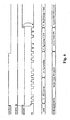
- Figures 5 to 8 each show some waveforms that illustrate different modes of functioning of the converter of Figure 4.
- The converter of Figure 3 comprises the same functional blocks (DAC, COMP, LOG) of the converter of Figure 1, but differs from the latter by virtue of the fact that the timing pulses that arrive at the terminal CK of the logic unit LOG come from a unit, indicated by CLK-MOD, that is capable of modifying the clock pulses arriving from the system clock (CLOCK) in response to control signals provided by the logic unit LOG via a bus indicated by REGBUS. More particularly, these control signals modify the period and/or the duty cycle of the clock pulses in a discrete manner, in steps equal to half a clock period, and on the basis of criteria defined in the logic unit.
- The converter of Figure 4 once again comprises some functional blocks equal to those of the converter of Figure 1, namely the blocks LOG, DAC and COMP, and also a clock pulse generator CLK-GEN, a generator of single pulses, in this example a monostable analog circuit MONOST, and an OR logic gate. It should only be noted that the logic unit LOG is provided with an additional output RESOSC for a signal that will stop the generator CLK-GEN and two outputs, REGBUS0 and REGBUS1, for regulating the operating parameters of the generator. It should also be noted that the logic unit LOG has a starting terminal, here indicated by RES, that also performs a resetting function, as will be explained further on. A converter equal to the one of Figure 4 is described in a patent application filed by the applicants on the same day as the present application and entitled "Analog-digital converter".
- The generator CLK-GEN has an output terminal OUT connected to the clock terminal CK of the logic unit LOG, an input activation terminal STOP connected to the output of the OR gate and two inputs connected to the logic unit by means of the two buses REGBUS0 and REGBUS1. The monostable circuit has an input terminal to which there is applied the conversion request signal CONVREQ and an output terminal GENRES connected to the starting and resetting input terminal RES of the logic unit and to an input terminal of the OR gate. The latter has a second input terminal connected to the output terminal RESOSC of the logic unit.
- The generator CLK-GEN and the quantization elements DAC and COMP are incorporated in one and the same integrated circuit. Preferably, the other circuit blocks of Figure 4 will also form part of the same integrated circuit.
- The generator CLK-GEN is a pulse generator that becomes active when a binary signal applied to its input STOP finds itself in a predetermined state of its two logic states and on its output terminal OUT produces an oscillation that can immediately be used because it is not affected by transitory phenomena. Furthermore, when the signal at its input terminal STOP switches to the other of the two logic states, it stops in a known condition, i.e. all its nodes always have the same predetermined binary values; therefore, when it is restarted (STOP=0), it does so with an oscillation of the correct value right from the first half-period. A generator of this type is described in European Patent Application No. 04425100.7 filed by applicants on 18 February 2004 under the title "Clock-pulse generator circuit".
- Let us now consider the functioning of the converter of Figure 4 with reference to the waveforms shown in Figure 5.
- Following a conversion request, the monostable circuit generates a pulse GENRES of a predetermined duration. In this example the pulse GENRES is produced when the signal CONVREQ applied as input to the monostable circuit switches from 0 to 1 and has a duration sufficient to set the logic unit LOG in its initial condition. In practice the signal GENRES brings a counter contained in the logic unit back to 0, sets the output RESOSC to 0 (for example, by means of a flip-flop which is controlled by the signal GENRES and maintains the set state also after the end of the signal GENRES) and prevents the activation of the oscillator for the whole of its duration. Indeed, it should be noted that the generator will not oscillate until STOP=1, i.e. both with RESOSC=1 and GENRES=1, while it will oscillate when STOP=0, i.e. only when the two inputs of the OR gate (RESOSC and GENRES) are both at 0. Be it noted also that in this way the start-up of the oscillator is delayed by a time equal to the duration of the pulse GENRES. When the pulse of the monostable circuit terminates (GENRES=0), the generator produces a clock signal CK that has a frequency and a duty cycle determined by the digital signals present on the buses REGBUS0 and REGBUS1, until such time as RESOSC returns to 1 and brings the generator to a halt (STOP=1) . During the activity of the generator the clock signal increases the contents of the counter of the logic unit LOG, giving rise to the successive emission of the signals needed to cause the quantization elements (DAC, COMP) to perform the operations, timed by the timing pulses, for the conversion of the analog input sample VIN into a digital code. Starting from an initial condition of deactivation (hold) of all the circuits, during which the consumption of the device is only such as is due to the leakage currents, the conversion is performed in accordance with the following phases:
- 1) ACDstart-up: activation of the analog parts of the converter (DAC, reference voltage source, comparator COMP, possible biasing circuits);
- 2) VINsampling: the voltage signal VIN to be
converted is loaded in the capacitors of the converter
DAC (
capacitor array 10 of Figure 2); - 3) VINstorage+SAR: the voltage VIN is memorized and the SAR procedure for the determination of the digital code corresponding to VIN is commenced;
- 4) Resultstorage+hold: the result is conveyed onto the output bus OUTBUS, the pulse generator is stopped and the analog parts are deactivated following an appropriate command of the logic unit.
-
- At the beginning of Phase 4) the last trailing edge of the clock signal assures that the counter of the logic unit LOG will cause the signal RESOSC to switch to 1 (and also assure the transfer of the digital code resulting from the conversion to the bus OUTBUS and the deactivation of the circuits). The generator will therefore have STOP=1 at the activation input, so that the output OUT remains at 0 and the clock signal stops after the pulse that brought about the condition RESOSC=1: from this it follows that the logic unit LOG will cease all activity on account of the lack of a clock signal. This state is maintained until a new leading edge of the conversion request signal CONVREQ. The number of clock pulses for each phase depends on the circuit characteristics and parameters.
- In the example described in relation to Figures 4 and 5 we considered a clock signal with a duty cycle of 50%. Nevertheless, this duty-cycle value, as also the frequency of the clock signal, may be changed arbitrarily, even while the generator is functioning, by appropriately changing the digital codes that the logic unit sends to the clock pulse generator on the buses bars REGBUS0 and REGBUS1.
- Similarly, in the example illustrated by Figure 3 the duty cycle and the period may be modified (discretely, in steps equal to half a period) by means of the digital signals sent by the logic unit LOG to the clock signal modification unit CLK-MOD via the bus REGBUS.
- The possibility of modifying the timing pulses, together with the fact that the time needed for the comparison operation performed by the comparator COMP is much shorter than half a period of the clock signal, implies considerable advantages in terms of energy saving. In fact, the logic unit LOG may be programmed for regulating the duty cycle of the timing pulses in such a way that more time will be accorded to the charging operations than to the comparison operations. For example, as shown in Figure 6, while the clock signal in Phases 1) and 2) has a duty cycle of 50%, in Phase 3) it has a duty cycle of 70% even though it maintains the same period. This behaviour is obtained by supplying to the generator CLK-GEN, via the bus bars REGBUS0 and
REGBUS 1, digital codes that determine a duty cycle of 50% in Phases 1), 2) and 4), and digital codes that determine a duty cycle of 70% in Phase 4) and, more precisely, digital codes that determine a clock signal that will maintain its high value for a longer time for the charging phases and its low value for a shorter period of time for the comparison phases. Thanks to this possibility of modifying the duty cycle, the buffer of the reference voltage may be designed with maximum performances inferior to those of a known converter, with the advantage of a smaller energy consumption in operation. - A further reduction of the consumption may be obtained by a further regulation of the duration of the clock signal during Phase 3). It should be noted that the consumption connected with the charging of the capacitors to the reference voltage VREF is directly proportional to the capacitances that have to be charged and inversely proportional to the time available for charging. Now, the maximum charging capacitance is associated with the first "attempt", i.e. with the charging of the capacitors for determining the most significant bit. The capacitances to be charged will thereafter reduce, halving on the occasion of each subsequent "attempt". If the clock signal is correspondingly modified to take account of this, one obtains a further significant reduction of the consumption of the buffer of the voltage VREF. Figure 7 shows the case in which the digital code applied to REGBUS1 is such as to prolong the duration of the high value of the clock signal up to 140% for the first "attempt", while maintaining the duty cycle at 70% for the remaining "attempts". If this were desirable, it would also be possible to diversify the durations for the subsequent "attempts", even though the advantages in terms of energy saving reduce very rapidly as the order number of the "attempts" increases.
- The converter and the method in accordance with the invention make it possible to eliminate or, at least, drastically reduce the noise and the offset that can be induced by parasite phenomena when relatively large currents are switched in the generator. The parasite phenomena are due to the inductances, resistances and capacitances associated with the connections between the integrated circuit and the terminals that connect it to the external circuits and can cause a damped oscillation on the supply voltages. A very critical phase of the functioning of the converter is the one in which the converter voltage VIN is memorized. If the edge of the clock pulse preceding the one used for the memorization generates an oscillation that has not yet been damped when the memorization edge arrives, the voltage VIN with respect to ground becomes altered, so that the memorized voltage is different from the one it is desired to convert. This problem is the more serious the higher the clock requency is. To avoid this happening, the half-period of the clock signal that precedes the memorization edge - as shown in Figure 8 - is lengthened, tripled for example. To this end the code applied to the bus REGBUS0, which determines the duration of the time during which the clock signal maintains its low value, is appropriately modified before the memorization edge, so that the memorization edge will arrive when the oscillation has been practically completely damped.
- As clearly brought out by what has been said above, the objects of the invention are fully attained, because with the described converter and method the electric energy necessary for performing the conversion can be determined without waste on the basis of the effective needs of each phase of the conversion and the noise normally associated with the switching of large currents in the clock generator can be practically eliminated.
- Although only some embodiments of the invention have here been illustrated and described, it is clear that numerous variants and modifications are possible without overstepping the inventive concept.
Claims (6)
- An analog-digital converter of the SAR type comprising:characterized in that the logic means (LOG) comprise means for producing regulation signals and that the timing pulse generator (CLK-MOD; CLK-GEN) comprises regulation means capable of modifying the duration and/or the frequency of the timing pulses in response to regulation signals (REGBUS; REGBUS0, REGBUS1) produced by the logic means.switched-capacitator quantization means (DAC, COMP) having an input for receiving an analog quantity to be converted (VIN);a register (REG) having an output (OUTBUS) for providing a digital quantity corresponding to the analog quantity;a timing pulse generator (CLK-MOD; CLK-GEN) andlogic means (LOG) connected to the quantization means (DAC, COMP), the register (REG) and the timing pulse generator (CLK-MOD; CLK-GEN), capable of responding to a conversion request signal (CONVREQ) by activating the quantization means in such a way that they will carry out predetermined operations timed by the timing pulses and load in the register (REG) the digital quantity to be furnished as output (OUTBUS),
- A method for converting an analog quantity (VIN) into a digital code (OUTBUS) by means of an analog-digital converter of the SAR type in accordance with Claim 1, wherein the predetermined operations timed by the timing pulses comprise the following phases:characterized in that the duration and/or the frequency of the timing pulses are modified during at least one of the phases indicated above in response to regulation signals emitted by the logic means (LOG).loading of the analog quantity to be converted (VIN) in the quantization means (DAC, COMP),memorization of the loaded analog quantity andidentification in the course of successive attempts, by means of operations of charging the capacitors and comparison in accordance with SAR technique, of the bit values of the digital code corresponding to the analog quantity to be converted,
- A method in accordance with Claim 2, wherein the duration of the timing pulses in the phase of identification by successive attempts is modified in such a way as to prolong the operations of charging the capacitors and to shorten the respective comparison operations.
- A method in accordance with Claim 3, wherein the frequency of the timing pulses is maintained unaltered
- A method in accordance with Claim 2, wherein the duration of the timing pulse in the operation of charging the capacitors for the first attempt is greater than the duration of the timing pulses for the subsequent attempts.
- A method in accordance with any one of Claims 2 to 5, wherein the duration of the half-period of the timing pulse that precedes the phase of identification by successive attempts is increased.
Priority Applications (4)
| Application Number | Priority Date | Filing Date | Title |
|---|---|---|---|
| DE200460007101 DE602004007101D1 (en) | 2004-04-01 | 2004-04-01 | Method and apparatus for analog-to-digital conversion of SAR type with low consumption and noise |
| EP04425241A EP1583244B1 (en) | 2004-04-01 | 2004-04-01 | Low consumption and low noise analog-digital converter of the SAR type and method of employing it |
| US11/097,455 US7106237B1 (en) | 2004-04-01 | 2005-04-01 | Low consumption and low noise analog-digital converter of the SAR type and method of employing it |
| US11/097,456 US7158069B2 (en) | 2004-04-01 | 2005-04-01 | Analog-digital converter |
Applications Claiming Priority (1)
| Application Number | Priority Date | Filing Date | Title |
|---|---|---|---|
| EP04425241A EP1583244B1 (en) | 2004-04-01 | 2004-04-01 | Low consumption and low noise analog-digital converter of the SAR type and method of employing it |
Publications (2)
| Publication Number | Publication Date |
|---|---|
| EP1583244A1 true EP1583244A1 (en) | 2005-10-05 |
| EP1583244B1 EP1583244B1 (en) | 2007-06-20 |
Family
ID=34878377
Family Applications (1)
| Application Number | Title | Priority Date | Filing Date |
|---|---|---|---|
| EP04425241A Expired - Lifetime EP1583244B1 (en) | 2004-04-01 | 2004-04-01 | Low consumption and low noise analog-digital converter of the SAR type and method of employing it |
Country Status (2)
| Country | Link |
|---|---|
| EP (1) | EP1583244B1 (en) |
| DE (1) | DE602004007101D1 (en) |
Cited By (2)
| Publication number | Priority date | Publication date | Assignee | Title |
|---|---|---|---|---|
| EP1916770A1 (en) * | 2006-10-26 | 2008-04-30 | Atmel Nantes Sa | Successive-approximation analog-to-digital converter, integrated circuit comprising such analog-to-digital converter, and corresponding method |
| EP4387105A1 (en) * | 2022-12-13 | 2024-06-19 | LX Semicon Co., Ltd. | Analog-to-digital converter and semiconductor device having the same |
Citations (4)
| Publication number | Priority date | Publication date | Assignee | Title |
|---|---|---|---|---|
| JPS5644225A (en) * | 1979-09-19 | 1981-04-23 | Matsushita Electric Ind Co Ltd | Analogue digital converter |
| EP0504805A2 (en) * | 1991-03-19 | 1992-09-23 | Fujitsu Limited | An analog-to-digital converter |
| US6329938B1 (en) * | 2000-06-15 | 2001-12-11 | Adaptec, Inc. | Programmable analog-to-digital converter with bit conversion optimization |
| US6556164B2 (en) * | 2000-01-28 | 2003-04-29 | Infineon Technologies Ag | Analog/digital converter and method for converting an analog input signal into a digital output signal |
-
2004
- 2004-04-01 EP EP04425241A patent/EP1583244B1/en not_active Expired - Lifetime
- 2004-04-01 DE DE200460007101 patent/DE602004007101D1/en not_active Expired - Lifetime
Patent Citations (4)
| Publication number | Priority date | Publication date | Assignee | Title |
|---|---|---|---|---|
| JPS5644225A (en) * | 1979-09-19 | 1981-04-23 | Matsushita Electric Ind Co Ltd | Analogue digital converter |
| EP0504805A2 (en) * | 1991-03-19 | 1992-09-23 | Fujitsu Limited | An analog-to-digital converter |
| US6556164B2 (en) * | 2000-01-28 | 2003-04-29 | Infineon Technologies Ag | Analog/digital converter and method for converting an analog input signal into a digital output signal |
| US6329938B1 (en) * | 2000-06-15 | 2001-12-11 | Adaptec, Inc. | Programmable analog-to-digital converter with bit conversion optimization |
Non-Patent Citations (1)
| Title |
|---|
| PATENT ABSTRACTS OF JAPAN vol. 005, no. 099 (E - 063) 26 June 1981 (1981-06-26) * |
Cited By (3)
| Publication number | Priority date | Publication date | Assignee | Title |
|---|---|---|---|---|
| EP1916770A1 (en) * | 2006-10-26 | 2008-04-30 | Atmel Nantes Sa | Successive-approximation analog-to-digital converter, integrated circuit comprising such analog-to-digital converter, and corresponding method |
| FR2907986A1 (en) * | 2006-10-26 | 2008-05-02 | Atmel Nantes Sa Sa | SUCCESSIVE APPROXIMATE ANALOGUE / DIGITAL CONVERTER, INTEGRATED COMPONENT AND CORRESPONDING CONVERSION METHOD. |
| EP4387105A1 (en) * | 2022-12-13 | 2024-06-19 | LX Semicon Co., Ltd. | Analog-to-digital converter and semiconductor device having the same |
Also Published As
| Publication number | Publication date |
|---|---|
| DE602004007101D1 (en) | 2007-08-02 |
| EP1583244B1 (en) | 2007-06-20 |
Similar Documents
| Publication | Publication Date | Title |
|---|---|---|
| US7106237B1 (en) | Low consumption and low noise analog-digital converter of the SAR type and method of employing it | |
| KR102778449B1 (en) | Symbol power tracking amplification system and wireless communication device including the same | |
| US8669896B2 (en) | Successive-approximation-register analog-to-digital convertor and related controlling method | |
| JP2019195168A (en) | Symbol power tracking amplification system and radio communication device including the same | |
| JP2012511284A (en) | Apparatus and method for gradual approach analog-to-digital conversion | |
| KR102889355B1 (en) | Digital-to-time converter circuit and method for operating the same | |
| US20120319788A1 (en) | Relaxation oscillator with low power consumption | |
| WO1999035741A1 (en) | Circuit and method for reducing sampling noise | |
| US10944418B2 (en) | Analog-to-digital converter capable of generate digital output signal having different bits | |
| US10727856B2 (en) | Successive approximation register analog-to-digital converter and control circuit thereof | |
| EP3565115A1 (en) | Symbol power tracking amplification system and a wireless communication device including the same | |
| CN108512538A (en) | Power inverter and its control circuit and control method | |
| US12224766B2 (en) | Analog digital converter and method for analog to digital converting in the analog digital converter | |
| CN105406868A (en) | Adaptive Clocking For Analog-to-digital Conversion | |
| EP1583244B1 (en) | Low consumption and low noise analog-digital converter of the SAR type and method of employing it | |
| Rahman et al. | Multimode digital SMPS controller IC for low-power management | |
| CN110034766B (en) | Comparator circuit and control method thereof | |
| US11824449B2 (en) | Switched-capacitor power stage and switched-capacitor converter | |
| US10345845B1 (en) | Fast settling bias circuit | |
| EP1583242B1 (en) | Analog-digital converter | |
| JP2001267925A (en) | Successive approximation type AD converter | |
| US7212143B1 (en) | Circuit for selectively analog signals into digital codes | |
| JP2011199403A (en) | Successive approximation a/d converter | |
| KR101808607B1 (en) | Reference voltage generation circuit and dc-dc converter using the same | |
| Lai | A 10-bit 40 MS/s successive approximation register analog-to-digital converter with Vcm-based method for wireless communications |
Legal Events
| Date | Code | Title | Description |
|---|---|---|---|
| PUAI | Public reference made under article 153(3) epc to a published international application that has entered the european phase |
Free format text: ORIGINAL CODE: 0009012 |
|
| AK | Designated contracting states |
Kind code of ref document: A1 Designated state(s): AT BE BG CH CY CZ DE DK EE ES FI FR GB GR HU IE IT LI LU MC NL PL PT RO SE SI SK TR |
|
| AX | Request for extension of the european patent |
Extension state: AL HR LT LV MK |
|
| 17P | Request for examination filed |
Effective date: 20060214 |
|
| AKX | Designation fees paid |
Designated state(s): DE FR GB IT |
|
| 17Q | First examination report despatched |
Effective date: 20060424 |
|
| GRAP | Despatch of communication of intention to grant a patent |
Free format text: ORIGINAL CODE: EPIDOSNIGR1 |
|
| GRAS | Grant fee paid |
Free format text: ORIGINAL CODE: EPIDOSNIGR3 |
|
| GRAA | (expected) grant |
Free format text: ORIGINAL CODE: 0009210 |
|
| AK | Designated contracting states |
Kind code of ref document: B1 Designated state(s): DE FR GB IT |
|
| REG | Reference to a national code |
Ref country code: GB Ref legal event code: FG4D |
|
| REF | Corresponds to: |
Ref document number: 602004007101 Country of ref document: DE Date of ref document: 20070802 Kind code of ref document: P |
|
| ET | Fr: translation filed | ||
| PLBE | No opposition filed within time limit |
Free format text: ORIGINAL CODE: 0009261 |
|
| STAA | Information on the status of an ep patent application or granted ep patent |
Free format text: STATUS: NO OPPOSITION FILED WITHIN TIME LIMIT |
|
| PG25 | Lapsed in a contracting state [announced via postgrant information from national office to epo] |
Ref country code: DE Free format text: LAPSE BECAUSE OF FAILURE TO SUBMIT A TRANSLATION OF THE DESCRIPTION OR TO PAY THE FEE WITHIN THE PRESCRIBED TIME-LIMIT Effective date: 20070921 |
|
| 26N | No opposition filed |
Effective date: 20080325 |
|
| REG | Reference to a national code |
Ref country code: FR Ref legal event code: PLFP Year of fee payment: 12 |
|
| REG | Reference to a national code |
Ref country code: FR Ref legal event code: PLFP Year of fee payment: 13 |
|
| REG | Reference to a national code |
Ref country code: FR Ref legal event code: PLFP Year of fee payment: 14 |
|
| PGFP | Annual fee paid to national office [announced via postgrant information from national office to epo] |
Ref country code: FR Payment date: 20170322 Year of fee payment: 14 |
|
| PGFP | Annual fee paid to national office [announced via postgrant information from national office to epo] |
Ref country code: GB Payment date: 20170324 Year of fee payment: 14 |
|
| PGFP | Annual fee paid to national office [announced via postgrant information from national office to epo] |
Ref country code: IT Payment date: 20170322 Year of fee payment: 14 |
|
| GBPC | Gb: european patent ceased through non-payment of renewal fee |
Effective date: 20180401 |
|
| PG25 | Lapsed in a contracting state [announced via postgrant information from national office to epo] |
Ref country code: GB Free format text: LAPSE BECAUSE OF NON-PAYMENT OF DUE FEES Effective date: 20180401 |
|
| PG25 | Lapsed in a contracting state [announced via postgrant information from national office to epo] |
Ref country code: FR Free format text: LAPSE BECAUSE OF NON-PAYMENT OF DUE FEES Effective date: 20180430 Ref country code: IT Free format text: LAPSE BECAUSE OF NON-PAYMENT OF DUE FEES Effective date: 20180401 |