TECHNICAL FIELD
The present invention relates to a Doherty amplifier, and more
particularly, to a Doherty amplifier, which has a gain compensator that is
disposed at a position ahead of a peak amplifier.
BACKGROUND ART
Due to the explosive proliferation of the portable terminal market
in recent years and improvements in the infrastructure associated therewith,
stricter requirements have been made from the market for improvements in
the efficiency of transmission amplifiers for base stations.
In order to respond to the foregoing requirements, attention has
been focused in recent years on the trend of attempts to build high-performance
and highly efficient amplifiers by combining technology to
amplify signals at high efficiency, as represented by the Doherty amplifier,
with technology to reduce distortions therefor together with recent distortion
compensation technology.
The Doherty amplifier is a device for improving the efficiency of a
high-output power amplifier, which was first proposed in Document 1 (W. H.
Doherty "A New High Efficiency Power Amplifier for Modulated Waves", Proc.
IRE, Vol. 24, No. 9, Sept. in 1936).
The Doherty amplifier comprises a carrier amplifier for performing
an amplifying operation at all times; and a peak amplifier for performing an
amplifying operation when high power is generated, specifically, only after
the carrier amplifier has reached a saturated maximum output.
In the Doherty amplifier, devices having the same characteristics
are generally used for the carrier amplifier and peak amplifier, and they are
arranged in parallel. A large number of Doherty amplifiers have been
actually implemented as amplifiers to handle signals in frequency bands from
low frequencies to millimeter waves.
The example described in Document 2 (JP-7-22852-A) is an
example of such a kind of Doherty amplifiers that is conventionally used.
Fig. 1 illustrates the Doherty amplifier described in Document 2. In the
following, the Doherty amplifier described in Document 2 will be described in
brief with reference to Fig. 1.
In Fig. 1, a signal applied from input terminal 1 is distributed to a
side of the carrier amplifier and to a side of the peak amplifier by input
branching circuit 2, which includes one-quarter wavelength transmission path
21. Carrier amplifier 3 amplifies a signal that is distributed to the carrier
amplifier side. A signal distributed to the peak amplifier side is amplified by
peak amplifier 4 after it has passed through one-quarter wavelength
transmission path 21f.
Output combiner circuit 5 includes one-quarter wavelength
transmission path 51. Output combiner circuit 5 combines the output of
carrier amplifier 3, which has passed one-quarter wavelength transmission
path 51, with the output of peak amplifier 4 to deliver the resulting output.
Therefore, a phase relationship between output signals of carrier amplifier 3
and peak amplifier 4 is identical at the signal combining point of output
combiner circuit 5.
However, if an amplifying operation of carrier amplifier 3 or peak
amplifier 4 of the Doherty amplifier differs from an ideal operation, the signal
combination, which is performed by output combiner circuit 5, is not
performed in an effective manner. For this reason, the Doherty amplifier fails
to provide an ideal linear amplifying action and saturated output power.
For example, the foregoing problem occurs when devices having
equivalent characteristics (for example, the gm-ld characteristic) are used for
a carrier amplifier and a peak amplifier, which make up the Doherty amplifier
(classical Doherty). In this event, a problem arises, particularly, in that the
operation of the peak amplifier differs from optimum performance.
Specifically, a problem occurs in that the gain in the peak amplifier is smaller
than a optimum gain.
Therefore, an ideal linear amplifying action or saturated output
power cannot be provided even if the carrier amplifier and peak amplifier are
identical in the gm (transfer conductance) characteristic (FET's or the like).
Several approaches for addressing this problem have been
proposed.
For example, Document 3 (RF Power Amplifiers for Wireless
communications, written by Steve C. Cripps, p236, Artech House, 1999) has
proposed a technique for controlling the attenuation amount of a variable
attenuator, which is disposed on the input side of a peak amplifier, in
accordance with the magnitude of the input level in order to compensate for
the transfer characteristic.
Also, Document 4 (Advanced Techniques in RF Power Amplifiers
written by Steve C. Cripps, P50, Artech House, 2002) has proposed a
method of generating maximum power of a Doherty amplifier by
appropriately controlling the bias setting of a carrier amplifier from a class-C
bias to a class-B bias, in accordance with an input signal level, though no
specific block diagram or the like is found therein.
Further, Document 5 (Published Japanese Translation of PCT
International Publication for Patent Application No. 2000-513535) has
proposed techniques by which a detector directly or indirectly detects the
power level of an input signal and the magnitude of the signal, such that bias
controllers of a carrier amplifier and a bias amplifier control biases for the
carrier amplifier and peak amplifier, respectively, relying on the detected
value.
However, whether it be the techniques of Documents 3, 4 or 5,
they all requires circuits for making determinations, control and the like, thus
leading to a problem that the configuration becomes complicated.
DISCLOSURE OF THE INVENTION
It is an object of the present invention to provide a Doherty
amplifier which is capable of accomplishing a linear amplifying and a power
combining operation closer to the ideal in a simple configuration, for example,
even if the same devices are used as a carrier amplifier and a peak amplifier.
To achieve the above object, a Doherty amplifier according to the
present invention has an input terminal, input branching means for
distributing the signal applied from the input terminal to a first path and a
second path, a carrier amplifier for amplifying the signal distributed to the first
path by the input branching means, a peak amplifier for amplifying the signal
of a predetermined level or higher among the signals distributed to the
second path by the input branching means, output combining means for
combining the output of the carrier amplifier with the output of the peak
amplifier, and a gain compensator, which is disposed at a position ahead of
the peak amplifier in the second path, for changing a gain in accordance with
the level of an inputted signal in order to correct the level of the signal
distributed to the second path.
The invention described above includes the gain compensator,
which is disposed at the position ahead of the peak amplifier in the second
path, for changing a gain in accordance with the level of an input signal in
order to correct the level of the signal distributed to the second path. Thus, it
is possible to compensate for the gain of the peak amplifier by a gain varying
operation of the gain compensator. It is therefore possible that circuits,
which have been conventionally required for performing detection,
determination, control and the like, are unnecessary. Consequently, it is
possible to carry out a linear amplifying and a power combining operation
closer to the ideal in a simple configuration. Since it is possible that a control
circuit, which has been conventionally required, is unnecessary, it is also
possible that dedicated control signals and dedicated terminals for the
control signals are unnecessary.
Also, in the Doherty amplifier according to the present invention, a
gain in the gain compensator, when a signal lower than the predetermined
level is applied, is different from a gain in the gain compensator when a
signal equal to or higher than the predetermined level is applied.
According to the invention described above, in the gain
compensator, the gain, when a signal lower than the predetermined level is
applied, is different from the gain when a signal equal to or higher than the
predetermined level is applied. Thus, in addition to the aforementioned
effects, the peak amplifier can be compensated for the gain when the peak
amplifier performs an amplifying operation, without changing the amplifying
operation start point of the peak amplifier for a signal applied from the input
terminal.
Also, in the gain compensator of the Doherty amplifier according
to the present invention, the gain, when the signal equal to or higher than the
predetermined level is applied, is larger than the gain when the signal lower
than the predetermined level is applied.
According to the present invention described above, in addition to
the aforementioned effects, the gain of the peak amplifier can be improved
when the peak amplifier performs an amplifying operation, without changing
the amplifying operation start point of the peak amplifier for a signal applied
from the input terminal. Consequently, when the gain in the peak amplifier is
smaller than an optimum gain, the gain in the peak amplifier can be
compensated for when the peak amplifier performs an amplifying operation,
without changing the amplifying operation start point of the peak amplifier.
Also, in the gain compensator of the Doherty amplifier according
to the present invention, the gain, when the signal equal to or higher than the
predetermined level is applied, is smaller than the gain when the signal lower
than the predetermined level is applied.
According to the invention described above, in addition to the
aforementioned effects, the gain of the peak amplifier can be reduced when
the peak amplifier performs an amplifying operation, without changing the
amplifying operation start point of the peak amplifier for a signal applied from
the input terminal. Consequently, when the gain in the peak amplifier is
larger than the ideal gain, the gain in the peak amplifier can be compensated
for when the peak amplifier performs an amplifying operation, without
changing the amplifying operation start point of the peak amplifier.
Also, in the Doherty amplifier according to the present invention,
the gain of the gain compensator is set based on the operation characteristic
of the peak amplifier. Thus, in addition to the aforementioned effects, the
gain in the peak amplifier can be compensated for with high accuracy.
Also, in the Doherty amplifier according to the present invention,
the gain compensator is a parallel circuit of an anti-parallel diode and a
resistor, or a parallel circuit of a diode and a resistor, or an FET, or a bipolar
transistor. Thus, in addition to the aforementioned effects, a simple
configuration can be used to implement the gain compensator.
Also, in the Doherty amplifier according to the present invention,
the carrier amplifier and peak amplifier are each composed of an FET, and
the gain compensator compensates for the gm characteristic of the peak
amplifier.
According to the invention described above, even when the carrier
amplifier and peak amplifier are composed of FET's, it is possible to provide
effects similar to the aforementioned effects.
BRIEF DESCRIPTION OF THE DRAWINGS
Fig. 1 is a block diagram illustrating a conventional Doherty
amplifier;
Fig. 2 is a block circuit diagram illustrating one embodiment of the
present invention;
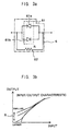
Fig. 3a is a circuit diagram illustrating an example of gain
compensator 6;
Fig. 3b is an explanatory diagram showing a characteristic of gain
compensator 6;
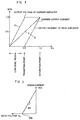
Fig. 4 is an explanatory diagram for describing operating states of
amplifiers 3 and 4 during an ideal operation of the Doherty amplifier;
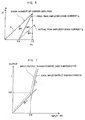
Fig. 5 is a characteristic diagram showing the drain current - gate
voltage characteristics of carrier amplifier 3 and peak amplifier 4;
Fig. 6 is an explanatory diagram illustrating an operating state of
the Doherty amplifier;
Fig. 7 is a characteristic diagram showing the characteristic of the
gain compensator illustrated in Fig. 3a;
Fig. 8 is an explanatory diagram showing an example of
compensation by the gain compensator in accordance with the peak
amplifier;
Fig. 9a is a circuit diagram illustrating another example of the gain
compensator;
Fig. 9b is a circuit diagram illustrating another example of the gain
compensator; and
Fig. 9c is a circuit diagram illustrating another example of the gain
compensator.
BEST MODE FOR CARRYING OUT THE INVENTION
In the following, embodiments of the present invention will be
described with reference to the drawings.
One feature of this embodiment is that gain compensator 6 is
disposed at a position ahead of peak amplifier 4, as illustrated in Fig. 2, in a
Doherty amplifier that includes carrier amplifier 3 and peak amplifier 4. In Fig.
2, a gain compensator, as a correcting means, has a gain that varies in
accordance with an input level. Note that in Fig. 2, those identical in
configuration to those illustrated in Fig. 1 are designated with the same
reference numerals.
This embodiment will be summarized here.
In the Doherty amplifier of this embodiment, gain compensator 6,
whose gain varies in accordance with an input level, is disposed in a
conventional configuration which comprises carrier amplifier 3, peak amplifier
4, output combiner 5, and input branching circuit 2, as illustrated in Fig. 1.
Specifically, as illustrated in Fig. 2, gain compensator 6 is disposed at a
position ahead of peak amplifier 4.
In this embodiment, when the level of an input signal is equal to or
higher than an amplification start level of peak amplifier 4 which is biased, for
example, to class C and composed of FET, gain compensator 6 makes a
correction such that it increases the gate input voltage signal of peak
amplifier 4.
By using gain compensator 6 as described above, even in a
Doherty amplifier has peak amplifier 4 and carrier amplifier 3 that have the
same characteristics, the Doherty amplifier can operate to generate a
desired maximum output at the time of a saturated output. It is therefore
possible to achieve optimum amplifying performance as a Doherty amplifier.
In the following, the Doherty amplifier of this embodiment will be
described specifically with reference to Fig. 2.
This Doherty amplifier has amplifier 3, generally called a "carrier
amplifier," which amplifies a signal at all times; and amplifier 4, generally
called a "peak amplifier" or an "auxiliary amplifier (in this specification, the
"peak amplifier" is always used), which operates only when a signal having a
predetermined level or higher is applied (only when high power is generated).
The predetermined level corresponds to the level of a signal that
is applied from input terminal 1 when carrier amplifier 3 starts generating
saturated output power. In this embodiment, the predetermined level is set
at the level of a signal applied from input terminal 1 when carrier amplifier 3
starts generating the saturated output power.
Gain compensator 6 is disposed at a position ahead of peak
amplifier 4 to compensate for an amplitude component of peak amplifier 4 in
accordance with the transfer characteristic (operation characteristic) of peak
amplifier 4.
Further, this Doherty amplifier includes output combiner circuit 5
as an output combining means for combining the output of carrier amplifier 3
with the output of peak amplifier 4 in order to deliver the combined output;
and input branching circuit 2 as an input branching means for distributing an
input signal to carrier amplifier 22 (first path) and the side of peak amplifier
23 (second path).
Generally, a Doherty amplifier has carrier amplifier 3 that operates
while maintaining saturation near the saturated output power. Thus, the
Doherty amplifier accomplishes a higher efficiency than general class-A and
class-AB amplifiers even when a backoff is removed from the saturated
power for delivery.
Generally, an amplifier, which is biased to class AB or class B, is
often used as carrier amplifier 3. Generally, peak amplifier 4 is often biased
to class C for use such that it operates only when a high-power signal is
generated.
Output combiner circuit 5, which combines the output of carrier
amplifier 3 with the output of peak amplifier 4, is composed, for example, of a
transformer, and generally comprises one-quarter wavelength transmission
line 51. Input branching circuit 2 includes one-quarter wavelength
transmission line 21 or a 90° hybrid circuit or the like for making a wave
relationship between an output signal of peak amplifier 4 and an output
signal of carrier amplifier 3 that is identical in pattern at a signal combining
point of output combiner circuit 5.
Also, gain compensator 6 of Fig. 2 is composed of anti-parallel
diode 61 and resistor 62, for example, as illustrated in Fig. 3a.
Specifically, a parallel circuit of anti-parallel diode 61 and resistor
62 may be used as gain compensator 6. Anti-parallel diode 61 is composed
of diode 61a and diode 61b. Diode 61a has a cathode that is connected to
one-quarter wavelength transmission line 21 of input branching circuit 2, and
a cathode that is connected to the input side of peak amplifier 4. Diode 61b
has a cathode that is connected to the anode of diode 61a, and an anode
that is connected to the cathode of diode 61a.
Because the operation principles of the general Doherty amplifier
are well known by those skilled in the art, for example, from documents such
as Advanced Techniques in RF Power Amplifiers, Artech House 2002 written
by Steve C. Cripps, detailed description thereon is omitted.
In the following, the operation of this embodiment will be
described.
For simplifying the description, this embodiment employs carrier
amplifier 3, which is biased to class B, and peak amplifier 4, which is biased
to class C, and employs FET devices of the same characteristics as carrier
amplifier 3 and peak amplifier 4. The operation of this Doherty amplifier will
be described below. However, the present invention is not limited to the
foregoing configuration, but can be modified as appropriate.
At first, the operating states of respective amplifiers 3, 4, in which
the Doherty amplifier achieves optimum performance, will be described with
reference to Fig. 4.
The operation of the Doherty amplifier is roughly divided into three
operation regions, specifically, a low level region, a transition region, and a
saturation region.
In Fig. 4, the horizontal axis represents input voltage Vin, which
indicates a maximum value of an input voltage, which is applied to each of
carrier amplifier 3 and peak amplifier 4, as 1, and the vertical axis represents
a drain current of peak amplifier 4 as Ip, an output voltage of carrier amplifier
3 as Vc, and a drain current of carrier amplifier 3 as Ic.
In this embodiment, assume that FET's of the same
characteristics are used as carrier amplifier 3 and peak amplifier 4. For this
reason, a maximum value of Ic and a maximum value of Ip are shown to be
equal. Also, peak amplifier 4, which is a component of a normal Doherty
amplifier, is biased to class C, and starts an amplifying operation only after
the drain current starts flowing from input voltage Vin that is 0.5.
Also, for the drain current gate voltage characteristics of the
respective devices, specifically, carrier amplifier 3 and peak amplifier 4,
assume that the drain current starts flowing from threshold voltage Vth, as
shown in Fig. 5, and transfer conductance gm has a constant value.
When signal Vin at a level equal to or lower than a predetermined
level (Vin=0.5 in this example) is applied to carrier amplifier 3 that is biased
to class B, output voltage Vc of carrier amplifier 3 is generated in proportion
to signal Vin. In this event, a region over which output voltage Vc of carrier
amplifier 3 varies in accordance with signal Vin, defines the low level region.
Next, when signal Vin reaches 0.5 (this is called the "transition
point"), carrier amplifier 3 is saturated, so that the output voltage becomes a
constant value. At this time, the efficiency of the Doherty amplifier itself is
maximized, where the efficiency ideally reaches 78 % (π/4) which is an ideal
efficiency of a class-B amplifier. However, the saturated output power of
carrier amplifier 3 at this time is one quarter of the saturated power that
should be generated as the Doherty amplifier.
When Vin increases from this transition point, peak amplifier 4
also starts operating.
With this operation of peak amplifier 4, a load impedance of
carrier amplifier 3 modulates through transmission transformer 51 of output
combiner circuit 5. As a result, the output current of carrier amplifier 3
increases linearly in accordance with the input voltage, so that a load is
supplied with larger power. As a result, in the Doherty amplifier, a linear
amplification characteristic is maintained. Consequently, the Doherty
amplifier can linearly amplify the power.
When the input voltage further increases, peak amplifier 4 also
reaches saturation. As a result, a saturated maximum output is generated as
the Doherty amplifier. For the time period from this transition point to a
saturation point, the total efficiency of the Doherty amplifier is maintained
extremely high.
The foregoing operation is an example of an ideal operation of the
Doherty amplifier.
In this event, the drain current of peak amplifier 4 must increase in
proportion to the input voltage, which is higher than the transition point, with
a slope twice as large as the slop of an increase in the drain current of
carrier amplifier 3. In this event, when the input voltage finally reaches a
peak (Vin=1.0), the drain current (Ic) of carrier amplifier 3 and the drain
current (Ip) of peak amplifier 4 are maximized (Ic=Ip=1.0). Consequently, the
load impedance, which is viewed from carrier amplifier 3, is also in an
optimal state in which the maximum output can be transferred to the load, so
that the maximum output of the Doherty amplifier can be generated.
Next, a description will be given of an actual operation of the
Doherty amplifier.
When the Doherty amplifier is actually designed, devices having
substantially the same characteristics are often used for carrier amplifier 3
and peak amplifier 4. This is a configuration called "classical Doherty."
For example, when the saturated power of a Doherty amplifier is
set at 100 W, the same devices, the saturated power of which is 50 W, are
used as a carrier amplifier and a peak amplifier. Of course, instead of this, a
configuration called "extended Doherty" may be used, in which the devices
differ in saturated power. However, because the basic principles are the
same, description and the like for that case are omitted.
However, when a Doherty amplifier is made up by using devices
which have the same characteristics as a carrier amplifier and a peak
amplifier as described above, ideal characteristics of the Doherty amplifier
cannot be accomplished just by simply combining the carrier amplifier with
the peak amplifier, having the same characteristics, as illustrated in Fig. 1 as
the prior art. For this reason, a lower coefficient, lower saturated power, and
degraded linearity will result near the saturated power.
Fig. 6 is a diagram showing an example of the degradation which
occurs in an actual Doherty amplifier, showing the input/output
characteristics of main parameters similar to the ideal state shown in Fig. 4.
As described above, in the ideal state, the current of peak
amplifier 4 must reach the maximum value at the maximum point of the input
voltage. Contrary to this, in the example shown in Fig. 6, transfer
conductance gm is only one-half of a value required as an ideal value. Thus,
even if the input voltage is maximized, the drain current merely reaches one-half
of an ideal value.
For this reason, an ideal operation of the Doherty amplifier fails.
According to a simple calculation, the drain efficiency at the maximum input
is 58.9 %, which is about 20 % lower than 78 % that occurs in the ideal state,
the output decreases to 50 % of the ideal state, and the input/output linearity
degrades to the output level that is 0.5 when the input is 1.
Thus, in the present invention, a Doherty amplifier that operates at
optimum performance can be implemented by disposing a gain compensator,
the gain of which varies in accordance with the magnitude of an input signal,
as an example illustrated in Fig. 3a, at a position ahead of peak amplifier 4.
For example, even if devices that have the same characteristics are used as
carrier amplifier 3 and peak amplifier 4, the resulting product can operate as
an ideal Doherty amplifier.
In the case of this embodiment, specifically, the characteristics of
gain compensator 6 shown in Fig. 3b may be set such that the output signal
increases substantially by a factor of two in response to an increase by one
of the input signal when signal Vin is at 0.5 or more, as shown in Fig. 7.
The characteristics as mentioned above can be approximately
accomplished by selecting appropriate diodes 61 a, 61 b and peripheral
resistor 62 in the exemplary circuit as illustrated in Fig. 3a. For example,
when a large resistance value is selected, the characteristic of the output
range, which shows a proportion that is occupied by the input/output
characteristic with a large slope, becomes large. Conversely, when a small
resistance value is selected, the characteristic on the output range, which
shows a proportion that is occupied by the input/output characteristic with a
large slope, becomes small.
Consequently, when this gain compensator 6 is disposed at a
position ahead of peak amplifier 4, and when the input level to gain
compensator 6 and an operating state are set such that the output range
start point of gain compensator 6 is positioned near the threshold voltage
(Vin=0.5) of peak amplifier 4 or at the threshold voltage (Vin=0.5) of peak
amplifier 4, the gm characteristic of peak amplifier 4 can be apparently
doubled, making use of a region in which the slope of the input/output
characteristic is approximately two.
Stated another way, peak amplifier 4 has a maximum drain
current at the time that the input level reaches the maximum value.
Therefore, it is possible to accomplish an ideal state of the Doherty amplifier
from the transition point to the saturated state. As such, even if the same
devices, for example, are used for the carrier amplifier and peak amplifier, it
is possible to implement a Doherty amplifier that can present a linear
amplifying and a power combining operation closer to the ideal in a simple
configuration.
Describing in greater detail, in the case of this example, the input
level to or the operating state of gain compensator 6 is set such that the gain
of gain compensator 6, i.e., the slope of the input/output characteristic of
gain compensator 6 is one or substantially one when the level of a signal
applied to input terminal 1 is equal to or lower than the threshold voltage of
peak amplifier 4, and the gain of gain compensator 6, i.e., the slope of the
input/output characteristic of gain compensator 6 is two or substantially two
when the level of the signal applied to input terminal 1 exceeds the threshold
voltage of peak amplifier 4. It is therefore possible to operate peak amplifier
4 in an ideal state.
As described above, gain compensator 6, the gain of which varies
in accordance with the level of an input signal, is disposed at the position
ahead of peak amplifier 4. Thus, it is possible to compensate for the gain
during the operation of the peak amplifier by a gain varying operation of gain
compensator 6. Also, it is possible to avoid an unintended operation of peak
amplifier 4 when there is no need for the peak amplifier to operate (in a state
where the level of a signal, which is applied to input terminal 1, is below the
predetermined level).
Supplementing this aspect, assume, for example, that the gain in
gain compensator 6 is fixed at a gain to compensate for peak amplifier 4
during its operation, then peak amplifier 4 can unexpectedly operate even in
a state where peak amplifier 4 should essentially not operate (in the state
where the level of a signal applied to input terminal 1 is below the
predetermined level).
On the contrary, in this embodiment, gain compensator 6, the gain
of which varies in accordance with the level of an input signal, is disposed at
a position ahead of peak amplifier 4. Thus, the gain of gain compensator 6
can be modified such that this gain goes to a gain at which the output of gain
compensator 6 is below the predetermined value at which peak amplifier 4
should essentially not operate (in the state where the level of a signal applied
to input terminal 1 is below the predetermined level), and the gain of gain
compensator 6 provides a gain which compensates the peak amplifier in the
state where the level of a signal applied to input terminal 1 is the same or
higher than the predetermined level. It is therefore possible to perform a
linear amplifying and a power combining operation closer to the ideal in a
simple configuration as described above.
Also, because the gain of gain compensator 6, when a signal that
is lower than the predetermined level is applied from input terminal 1, is set
different from the gain of gain compensator 6 when a signal that is equal to
or higher than the predetermined level is applied, the linear amplifying and
power combining operations closer to the ideal can be performed in a simple
configuration, as described above, without changing the amplifying operation
start point of peak amplifier 4 (the threshold voltage of peak amplifier 4) for
the signal applied from input terminal 1.
Also, when the gain of gain compensator 6, when a signal equal
to or higher than the predetermined level, is larger than the gain of gain
compensator 6 when a signal lower than the predetermined level is applied,
the gain of the peak amplifier, when the peak amplifier performs an
amplifying operation, can be increased to an ideal gain without changing the
amplifying operation start point of the peak amplifier for the signal applied
from the input terminal, if the gain of peak amplifier 4 is below the ideal value.
As well, the gain of gain compensator 6 is set based on the
operation characteristic of peak amplifier 6. Thus, in addition to the
aforementioned effects, the gain of peak amplifier 6 and/or the amplifying
operation start point of peak amplifier 6 (the threshold voltage in this
example) can be compensated for with high accuracy.
In the foregoing, an example has been shown for the case where
transfer conductance gm of peak amplifier 4 is just one-half as much as a
value that would be required as an ideal value, and an example has been
shown for the case where the slope of the input/output characteristic of gain
compensator 6 is set to two or approximately two as the gain compensation
of gain compensator 6, when signal Vin is equal to or more than 0.5.
However, the gain compensation of gain compensator 6 when signal Vin is
equal to or more than 0.5 can be changed as appropriate depending on the
ratio of transfer conductance gm of peak amplifier 4 to the ideal value.
For example, when transfer conductance gm of peak amplifier 4 is
larger than the value required as the ideal value, the slope of the input/output
characteristic of gain compensator 6 may be set to one or approximately one,
as the gain compensation of gain compensator 6, if signal Vin is less than
0.5. On the other hand, if signal Vin is equal to or more than 0.5, the slope
of the input/output characteristic of gain compensator 6 may be reduced to
less than one, as the gain compensation of gain compensator 6.
As described above, when using gain compensator 6, whose gain
is smaller, when a signal equal to or higher than a predetermined level is
applied, than the gain, when a signal lower than the predetermined level is
applied, the gain of the peak amplifier can be reduced when the peak
amplifier performs an amplifying operation, without changing the amplifying
operation start point of the peak amplifier to the signal that is applied from
the input terminal. Thus, when the gain of the peak amplifier is larger than
the ideal gain, the peak amplifier can be compensated for this gain when the
peak amplifier performs an amplifying operation, without changing the
amplifying operation start point of the peak amplifier.
Also, the gain compensator is not limited to the configuration
illustrated in Fig. 3a, but can be modified as appropriate. For example, gain
compensator 6 can also be implemented by a simple circuit as illustrated in
Fig. 9 which has characteristics as described above.
Fig. 9 will be described in brief. Fig. 9a is a diagram illustrating an
example in which a parallel circuit of diode 63 and resistor 64 are used as
gain compensator 6. In Fig. 9a, diode 63 has a cathode that is connected to
one-quarter wavelength transmission line 21 of input branching circuit 2, and
diode 63 has an anode that is connected to the input side of peak amplifier 4.
Fig. 9b is a diagram illustrating an example in which FET 65 is used as gain
compensator 6. In Fig. 9b, FET 65 has a drain that is connected to second
path 23, and the FET has a grounded source. Fig. 9c illustrates an example
in which bipolar transistor 66 is used as gain compensator 6. In Fig. 9c,
bipolar transistor 66 has a collector that is connected to second path 23,
bipolar transistor 66 has a grounded emitter, and desired voltage VB is
applied to the base of bipolar transistor 66.
Also, the concept of the present invention can be readily extended
to amplifiers having different saturated current characteristics of devices that
are used for peak amplifier 4 and carrier amplifier 3. For example, even
when devices, which differ in source voltage or saturated current
characteristic, are used as peak amplifier 4 and carrier amplifier 3, an
approach substantially identical to the foregoing can be basically employed,
by taking into consideration of the input/output characteristic which is
normalized by a maximum value, as described above. To give a specific
illustration, as shown in Fig. 8, a slope of the peak amplifier, from a class-C
bias point to an operating current value, in which the desired saturated
output power can be generated, may be corrected by the gain compensator
using a desired value. In particular, a slope of the peak amplifier, from its
amplifying operation start point (for example, the threshold voltage) to the
operating current value in which the desired saturated output power can be
generated, for example, the gm characteristic, may be corrected by the gain
compensator using a desired value.
Therefore, even when devices, which have different
characteristics from each other, are used as carrier amplifier 3 and peak
amplifier 4, it is possible to implement a Doherty amplifier which provides a
linear amplifying and a power combining operation close to the ideal in a
simple configuration.
In the present invention, the gain compensator, whose gain varies
in accordance with the level of an input signal, is disposed at a position
ahead of the peak amplifier of the Doherty amplifier. It is therefore possible
to perform an ideal amplifying operation at optimum performance without
requiring a complicated circuit configuration and control for performing
detection, determination, control and the like, as is the case with the prior art.
Consequently, it is possible to simplify the configuration and reduce the cost
even when the same devices, for example, are used as the carrier amplifier
and peak amplifier.
In the embodiment described above, the illustrated configurations
are mere examples, and the present invention is not limited to the
configurations.