EP1583104A2 - Nanometric mechanical oscillator, method of fabricating the same, and measurement apparatus using the same - Google Patents
Nanometric mechanical oscillator, method of fabricating the same, and measurement apparatus using the same Download PDFInfo
- Publication number
- EP1583104A2 EP1583104A2 EP05005173A EP05005173A EP1583104A2 EP 1583104 A2 EP1583104 A2 EP 1583104A2 EP 05005173 A EP05005173 A EP 05005173A EP 05005173 A EP05005173 A EP 05005173A EP 1583104 A2 EP1583104 A2 EP 1583104A2
- Authority
- EP
- European Patent Office
- Prior art keywords
- oscillator
- mass
- sample
- nanometric mechanical
- base
- Prior art date
- Legal status (The legal status is an assumption and is not a legal conclusion. Google has not performed a legal analysis and makes no representation as to the accuracy of the status listed.)
- Withdrawn
Links
Images













Classifications
-
- G—PHYSICS
- G01—MEASURING; TESTING
- G01P—MEASURING LINEAR OR ANGULAR SPEED, ACCELERATION, DECELERATION, OR SHOCK; INDICATING PRESENCE, ABSENCE, OR DIRECTION, OF MOVEMENT
- G01P15/00—Measuring acceleration; Measuring deceleration; Measuring shock, i.e. sudden change of acceleration
-
- B—PERFORMING OPERATIONS; TRANSPORTING
- B81—MICROSTRUCTURAL TECHNOLOGY
- B81B—MICROSTRUCTURAL DEVICES OR SYSTEMS, e.g. MICROMECHANICAL DEVICES
- B81B3/00—Devices comprising flexible or deformable elements, e.g. comprising elastic tongues or membranes
-
- G—PHYSICS
- G01—MEASURING; TESTING
- G01P—MEASURING LINEAR OR ANGULAR SPEED, ACCELERATION, DECELERATION, OR SHOCK; INDICATING PRESENCE, ABSENCE, OR DIRECTION, OF MOVEMENT
- G01P15/00—Measuring acceleration; Measuring deceleration; Measuring shock, i.e. sudden change of acceleration
- G01P15/02—Measuring acceleration; Measuring deceleration; Measuring shock, i.e. sudden change of acceleration by making use of inertia forces using solid seismic masses
- G01P15/08—Measuring acceleration; Measuring deceleration; Measuring shock, i.e. sudden change of acceleration by making use of inertia forces using solid seismic masses with conversion into electric or magnetic values
-
- G—PHYSICS
- G01—MEASURING; TESTING
- G01P—MEASURING LINEAR OR ANGULAR SPEED, ACCELERATION, DECELERATION, OR SHOCK; INDICATING PRESENCE, ABSENCE, OR DIRECTION, OF MOVEMENT
- G01P15/00—Measuring acceleration; Measuring deceleration; Measuring shock, i.e. sudden change of acceleration
- G01P15/02—Measuring acceleration; Measuring deceleration; Measuring shock, i.e. sudden change of acceleration by making use of inertia forces using solid seismic masses
- G01P15/08—Measuring acceleration; Measuring deceleration; Measuring shock, i.e. sudden change of acceleration by making use of inertia forces using solid seismic masses with conversion into electric or magnetic values
- G01P15/097—Measuring acceleration; Measuring deceleration; Measuring shock, i.e. sudden change of acceleration by making use of inertia forces using solid seismic masses with conversion into electric or magnetic values by vibratory elements
-
- G—PHYSICS
- G01—MEASURING; TESTING
- G01Q—SCANNING-PROBE TECHNIQUES OR APPARATUS; APPLICATIONS OF SCANNING-PROBE TECHNIQUES, e.g. SCANNING PROBE MICROSCOPY [SPM]
- G01Q20/00—Monitoring the movement or position of the probe
- G01Q20/02—Monitoring the movement or position of the probe by optical means
-
- G—PHYSICS
- G01—MEASURING; TESTING
- G01Q—SCANNING-PROBE TECHNIQUES OR APPARATUS; APPLICATIONS OF SCANNING-PROBE TECHNIQUES, e.g. SCANNING PROBE MICROSCOPY [SPM]
- G01Q20/00—Monitoring the movement or position of the probe
- G01Q20/04—Self-detecting probes, i.e. wherein the probe itself generates a signal representative of its position, e.g. piezoelectric gauge
-
- G—PHYSICS
- G01—MEASURING; TESTING
- G01Q—SCANNING-PROBE TECHNIQUES OR APPARATUS; APPLICATIONS OF SCANNING-PROBE TECHNIQUES, e.g. SCANNING PROBE MICROSCOPY [SPM]
- G01Q60/00—Particular types of SPM [Scanning Probe Microscopy] or microscopes; Essential components thereof
- G01Q60/24—AFM [Atomic Force Microscopy] or apparatus therefor, e.g. AFM probes
- G01Q60/32—AC mode
-
- G—PHYSICS
- G01—MEASURING; TESTING
- G01Q—SCANNING-PROBE TECHNIQUES OR APPARATUS; APPLICATIONS OF SCANNING-PROBE TECHNIQUES, e.g. SCANNING PROBE MICROSCOPY [SPM]
- G01Q60/00—Particular types of SPM [Scanning Probe Microscopy] or microscopes; Essential components thereof
- G01Q60/24—AFM [Atomic Force Microscopy] or apparatus therefor, e.g. AFM probes
- G01Q60/38—Probes, their manufacture, or their related instrumentation, e.g. holders
-
- G—PHYSICS
- G01—MEASURING; TESTING
- G01Q—SCANNING-PROBE TECHNIQUES OR APPARATUS; APPLICATIONS OF SCANNING-PROBE TECHNIQUES, e.g. SCANNING PROBE MICROSCOPY [SPM]
- G01Q70/00—General aspects of SPM probes, their manufacture or their related instrumentation, insofar as they are not specially adapted to a single SPM technique covered by group G01Q60/00
- G01Q70/06—Probe tip arrays
-
- H—ELECTRICITY
- H03—ELECTRONIC CIRCUITRY
- H03H—IMPEDANCE NETWORKS, e.g. RESONANT CIRCUITS; RESONATORS
- H03H9/00—Networks comprising electromechanical or electro-acoustic elements; Electromechanical resonators
- H03H9/02—Details
- H03H9/02244—Details of microelectro-mechanical resonators
-
- B—PERFORMING OPERATIONS; TRANSPORTING
- B82—NANOTECHNOLOGY
- B82Y—SPECIFIC USES OR APPLICATIONS OF NANOSTRUCTURES; MEASUREMENT OR ANALYSIS OF NANOSTRUCTURES; MANUFACTURE OR TREATMENT OF NANOSTRUCTURES
- B82Y10/00—Nanotechnology for information processing, storage or transmission, e.g. quantum computing or single electron logic
-
- B—PERFORMING OPERATIONS; TRANSPORTING
- B82—NANOTECHNOLOGY
- B82Y—SPECIFIC USES OR APPLICATIONS OF NANOSTRUCTURES; MEASUREMENT OR ANALYSIS OF NANOSTRUCTURES; MANUFACTURE OR TREATMENT OF NANOSTRUCTURES
- B82Y20/00—Nanooptics, e.g. quantum optics or photonic crystals
-
- B—PERFORMING OPERATIONS; TRANSPORTING
- B82—NANOTECHNOLOGY
- B82Y—SPECIFIC USES OR APPLICATIONS OF NANOSTRUCTURES; MEASUREMENT OR ANALYSIS OF NANOSTRUCTURES; MANUFACTURE OR TREATMENT OF NANOSTRUCTURES
- B82Y30/00—Nanotechnology for materials or surface science, e.g. nanocomposites
-
- G—PHYSICS
- G11—INFORMATION STORAGE
- G11B—INFORMATION STORAGE BASED ON RELATIVE MOVEMENT BETWEEN RECORD CARRIER AND TRANSDUCER
- G11B9/00—Recording or reproducing using a method not covered by one of the main groups G11B3/00 - G11B7/00; Record carriers therefor
- G11B9/12—Recording or reproducing using a method not covered by one of the main groups G11B3/00 - G11B7/00; Record carriers therefor using near-field interactions; Record carriers therefor
- G11B9/14—Recording or reproducing using a method not covered by one of the main groups G11B3/00 - G11B7/00; Record carriers therefor using near-field interactions; Record carriers therefor using microscopic probe means, i.e. recording or reproducing by means directly associated with the tip of a microscopic electrical probe as used in Scanning Tunneling Microscopy [STM] or Atomic Force Microscopy [AFM] for inducing physical or electrical perturbations in a recording medium; Record carriers or media specially adapted for such transducing of information
- G11B9/1418—Disposition or mounting of heads or record carriers
Definitions
- the present invention relates to a nanometric mechanical oscillator, a method of fabricating the same, and a measurement apparatus using the same.
- the scanning force microscope was invented by Gerd Binnig, et al . around 1986 (above-mentioned literature 1). Subsequently, in the mid to late 1980s, T. Albrecht, Calvin Quate, et al . developed a strip-shaped cantilever having a length of a few hundreds of microns and having at its tip a probe having a height of about 3 ⁇ m. The cantilever was fabricated from silicon or silicon nitride. Since the mid to late 1980s, cantilevers of the above-described configuration have been sold in the market.
- Measurement of variations in the amplitude of vibration and characteristic frequency of a mechanical oscillator enables detection of variation in the mass of the oscillator and variation of a field in which the oscillator is placed.
- the force detection resolution obtained by use of a mechanical oscillator increases when its characteristic frequency or quality factor increases and when its spring constant or temperature is lowered.
- reducing the size of the oscillator advantageously increases sensitivity.
- an object of the present invention is to provide a stable and highly sensitive nanometric mechanical oscillator having a considerably high detection resolution that enables detection of variation in force or mass on the nanometer order, as well as a method of fabricating the same, and a measurement apparatus using the same.
- the present invention provides the following.
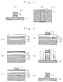
- FIG. 1 includes views showing a nanometric mechanical oscillator according to a first embodiment of the present invention.
- FIG. 2 includes cross-sectional views showing steps of fabricating the nanometric mechanical oscillator.
- a rectangular nanometric mechanical oscillator 1 includes a base 2, a rectangular oscillator mass 4, and a neck portion 3 having elasticity and connecting the base 2 and the rectangular oscillator mass 4.
- the neck portion 3 has a rectangular cross section as viewed along a vertical direction.
- the oscillator can be fabricated such that the rectangular oscillator mass 4 has a thickness of 60 nm and the neck portion 3 has a height of 100 nm.
- the diameter of the rectangular oscillator mass 4 is determined by the dimension of the mask 7, and the size of the neck portion 3 is determined by the time over which hydrofluoric acid etching is performed.
- an oscillator whose rectangular oscillator mass 4 has a width of about 500 nm and whose neck portion 3 has a width of about 50 nm.
- the nanometric mechanical oscillator fabricated as described above can be oscillated easily along an x-axis direction but cannot be oscillated easily along a y-axis direction. Therefore, when the mechanical oscillator is to be used as a sensor or actuator, detection and positioning by use of its anisotropy becomes possible.
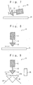
- FIG. 3 shows a case in which the nanometric mechanical oscillator is applied to a scanning force microscope.
- a sample 8 assuming the form of a thin film is fabricated on the rectangular oscillator mass 4, which is an oscillator surface, and probing is performed by use of a stationary probe 9.
- an array-type rectangular mechanical oscillator 1 can be applied to a gas sensor of high sensitivity.
- each rectangular oscillator mass 4 is coated with an arbitrary functional thin film. When the thin film absorbs a specific substance, a resultant change in mechanical oscillation frequency can be detected.
- FIG. 4 is a view showing a nanometric mechanical oscillator according to a second embodiment of the present invention.
- FIG. 5 includes cross-sectional views showing steps of a first method of fabricating the nanometric mechanical oscillator according to the second embodiment of the present invention.
- a nanometric mechanical oscillator 10 includes a base 11, a tetrahedral oscillator mass 13, and a neck portion 12, which connects the base 11 and the tetrahedral oscillator mass 13 and serves as an elastic portion.
- the mechanical oscillator 10 assumes a mushroom-like shape and has a nanometric size.
- the oscillator mass 13 assumes a tetrahedral shape, and therefore is suitably used as a probe of a scanning force microscope in such a manner that the oscillator mass 13 is caused to approach an arbitrary sample surface to thereby observe the surface state.
- FIG. 6 includes cross-sectional views showing steps of a second method of fabricating the nanometric mechanical oscillator according to the second embodiment of the present invention.
- this fabrication method is not limited to the case where a bonded substrate composed of a silicon substrate and a silicon oxide film is used.
- An oscillator-like structure having a head portion and a neck portion can be fabricated by use of a bonded substrate of a different type, provided that the substrate and film of the bonded substrate are formed of different materials and exhibit different properties in relation to processing such as etching or removal through application of heat.
- a bonded substrate composed of a quartz substrate and a silicon film or a bonded substrate composed of a quartz crystal substrate and a silicon film is used, introduction of light from the back face or excitation of an oscillator by use of the piezo effect of the base thereof becomes possible.
- a fabrication method similar to that shown in FIG. 5 can be used. However, in order to protect quartz (crystal substrate) from etching of silicon oxide by use of hydrofluoric acid, a silicon layer having a thickness of a few nm to a few tens of nm is provided.
- the nanometric mechanical oscillator obtained in the above-described manner has the following possible applications.
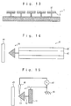
- FIG. 13 is a view showing a nanometric mechanical oscillator according to a third embodiment of the present invention.
- an nanometric mechanical oscillator 1 has a large number of oscillator masses 3 arranged in a matrix pattern; and a functional thin film 37 capable of reacting with a specific substance or absorbing a specific substance is applied to each of the oscillator masses 3 by means of, for example, vapor deposition.
- the nanometric mechanical oscillator 1 can be used to obtain a measurement apparatus for detecting the presence and concentration of a trace substance in a gas sample.
- FIG. 14 is a view showing a nanometric mechanical oscillator according to a fourth embodiment of the present invention.
- a nanometric mechanical oscillator 10 is disposed at the tip of an optical fiber 41 to face a sample 44.
- Reference numeral 42 denotes a fiber core
- 43 denotes a fiber cladding.
- FIG. 15 is a view showing a nanometric mechanical oscillator according to a fifth embodiment of the present invention.
- a nanometric mechanical oscillator 10 is grounded at 45; and an electron beam emitted from an apparatus (electrode) 46 is radiated on the nanometric mechanical oscillator 10, while being focused to have a diameter on the nanometer order.
- the mechanical oscillator 10 has electrical conductivity to its base 11, and a portion of the mechanical oscillator 10 exhibits a piezo effect.
- the mechanical oscillator causes self-excited oscillation due to current flowing upon radiation of the electron beam and deformation of the oscillator due to the current. Variation in the current flowing out of the oscillator 10 is detected by a high-frequency current detector 47 in order to detect the amplitude and frequency of oscillation of the oscillator 10.
- Reference numeral 48 denotes a sample.
- a tungsten-filament-type electron beam source or field emission of a commercially available ordinary scanning electron microscope is used as an electron beam source; and the generated electron beam is focused by use of an electromagnetic lens system.
- FIG. 16 is a view showing a nanometric mechanical oscillator according to a sixth embodiment of the present invention.
- a nanometric mechanical oscillator 10 is provided on a nearfield light generation surface 51A of a solid immersion lens 51 such that an oscillator mass 13 faces a sample 53.
- a laser beam is introduced into the solid immersion lens 51 via a lens 52 and is then returned in the opposite direction.
- a spot of light focused to a degree beyond a bendable limit is formed in the base of the nanometric mechanical oscillator 10.
- the amplitude and frequency of oscillation of the oscillator 10 can be detected on the basis of the return light.
- the below-listed studies are known.
- FIG. 17 is a view showing a nanometric mechanical oscillator according to a seventh embodiment of the present invention.
- a laminated substrate composed of a substrate 61, a dielectric gap layer 62, a mask layer (Sb) 63, and a dielectric layer (gap layer) 64 is provided; and a nanometric mechanical oscillator 10 is disposed on the dielectric layer (gap layer) 64.
- a sample 65 is disposed in front of the mechanical oscillator 10.
- a laser beam 66 is radiated onto the back face of the substrate 61 via a lens 67.
- the nanometric mechanical oscillator 10 is fixed onto the laminated substrate having the mask layer 63 formed of Sb.
- the laminated substrate is called Super-RENS (Supper-resolution Near-field Structure).
- Super-RENS Supper-resolution Near-field Structure
- a laser beam is radiated onto the mask layer 63, a portion of the mask changes, with resultant establishment of a state equivalent to formation of an opening on the nanometer order. This enables detection of oscillation of the nanometric mechanical oscillator 10 only to thereby reduce background noise.
- a reference for the Super-RENS is J. Tominaga, et al . Appl. Phys. Lett. 73, 2078 (1988).
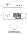
- FIG. 18 includes views showing a nanometric mechanical oscillator according to an eighth embodiment of the present invention, wherein FIG. 18(a) is a side view of the oscillator, and FIG. 18(b) is a top view of the oscillator.
- reference numeral 71 denotes a quartz-crystal substrate (or silicon substrate having a piezo thin film); 72 denotes comb-shaped electrodes; and 73 denotes an AC voltage source connected to the comb-shaped electrodes 72.
- FIG. 19 is a view showing a nanometric mechanical oscillator according to a ninth embodiment of the present invention.
- reference numeral 81 denotes a base; and 82 denotes a particle moving toward a nanometric mechanical oscillator 10.
- the oscillator mass 13 is displaced in accordance with the law of conservation of momentum, because the oscillator mass 13 is small. Through detection of the displacement, the velocity of the particle can be detected. That is, a particle-velocity detection apparatus can be obtained.
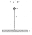
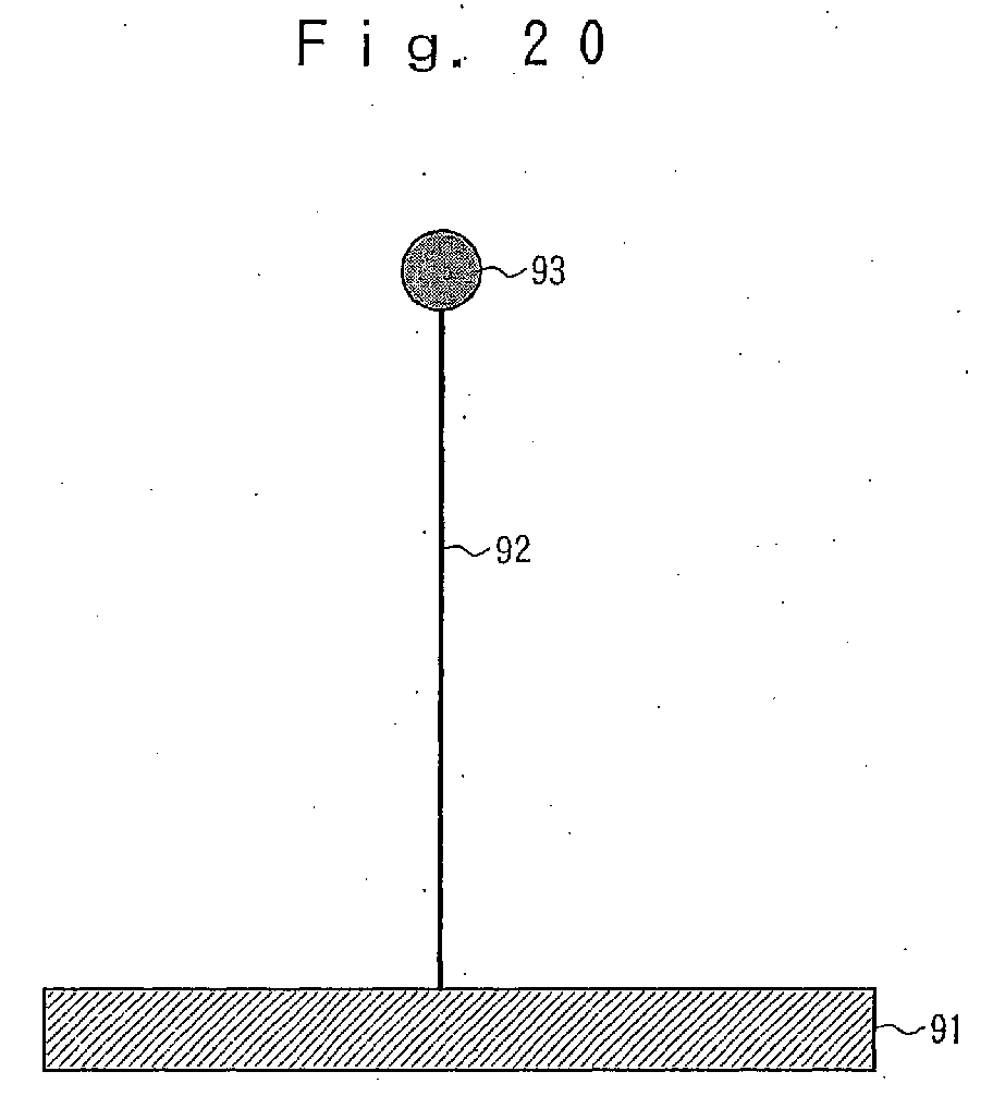
- FIG. 20 is a view showing a nanometric mechanical oscillator according to a tenth embodiment of the present invention.
- reference numeral 91 denotes a base
- 92 denotes a columnar, elastic neck portion formed of a very thin, long silicon whisker, which is fabricated in accordance with an LPCVD (low-pressure CVD) method to have a diameter on the order of 10 nm and a length on the order of one micron to one millimeter
- 93 denotes a gold sphere (optionally coated with a magnetic material such as cobalt or nickel) provided at the tip of the neck portion 92.
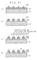
- FIG. 21 includes cross-sectional views showing steps of fabricating a nanometric mechanical oscillator according to an eleventh embodiment of the present invention.
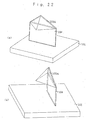
- FIG. 22 includes enlarged perspective views of the nanometric mechanical oscillator, wherein FIG. 22(a) is a front view, and FIG. 22(b) is a side view.
- FIG. 23 includes perspective views of a microcapsule, wherein FIG. 23(a) is a front view, and FIG. 23(b) is a side view.
- silicon or metal is vapor-deposited on a structure, which is formed from silicon and silicon oxide with very small variation in size and which serves as a nucleus; and subsequently, the oxide silicon is removed. Therefore, a single probe can be fabricated or a large number of probes can be fabricated simultaneously in such a manner that each probe has an opening having an accurately controlled size.
- the tetrahedral probe supported by the thin-film elastic portion (neck portion) formed through oblique vapor deposition can be used in a scanning force microscope in such a manner that an apex or a corner located apart from the support portion serves as a probe tip.
- a capsule having the very small opening 105 as shown in FIG. 23 can be fabricated to have a size on the order of 10 nm to 1 ⁇ m and can be used for an opening for capturing a sample or for generating a photo nearfield.
- FIG. 24 includes configurational views of a nanometric mechanical oscillator according to a twelfth embodiment of the present invention, wherein FIG. 24(a) is a top view of a first layer, FIG. 24(b) is a top view of a second layer, FIG. 24(c) is a front view of the entire oscillator, and FIG. 24(d) is a side view of the entire oscillator.
- the first layer 111 (FIG. 24(a)) includes a piezo substrate 112, a surface-acoustic-wave generation unit (formed on the reverse side) 113, and depressions 114 formed in the piezo substrate 112 at locations corresponding to a large number of arrayed cantilevers having probes.
- the second layer 115 has a base portion 116 and a large number of arrayed cantilevers 117 projecting from the base portion 116 and having probes 118.
- the first layer 111 and the second layer 115 are superposed on each other to thereby obtain an element 110 as shown in FIGS. 24(c) and 24(d).
- element 110 surface acoustic waves are generated within the piezo substrate 112 along two directions in a plane to thereby cause the probes to sequentially approach a measurable region of a sample.
- FIG. 25 is a configurational view of a measurement system for measuring a sample by use of an element having a large number of arrayed cantilevers having probes, which was fabricated as shown in FIG. 24.
- reference numeral 121 denotes a sample table; and 122 denotes a sample placed on the sample table 121.
- the sample 122 is measured in such a manner that the element 110 equipped with the large number of arrayed cantilevers 117 having the probes 118 is caused to sequentially approach a measurable region of the sample 122.
- the measurement system includes a lens system 123, a laser 124, a half mirror 125, a CCD camera 126, and a video display 127 connected to the CCD camera 126 and serving as a display unit.
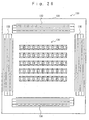
- FIG. 26 is a top view of the substrate of an element having a large number of arrayed cantilevers according to a modification of the twelfth embodiment of the present invention.
- the element 130 includes a piezo substrate 131; surface-acoustic-wave generation units 132, 133, 134, and 135 formed along the four sides of the piezo substrate 131 (formed on the reverse surface); and a large number of cantilevers 136 arrayed in a matrix at the center portion of the piezo substrate 131.
- FIG. 26 shows an example in which cantilevers are arranged two-dimensionally to form a 5 x 10 matrix.
- an interference cavity corresponding to each cantilever imparts brightness to a corresponding pixel, so that the shape and characteristics of the sample can be visualized as a whole, as is apparent from the explanatory view of FIG. 27.
- FIG. 28 is a schematic view of a nanometric mechanical oscillator according to a thirteenth embodiment of the present invention.
- a large number of nanometric mechanical oscillators 142 are arrayed on a substrate 141 formed of a piezo material.
- Surface acoustic waves are caused to propagate along two directions in a plane, so that the probes 143 are caused to sequentially approach a measurable region of the sample 143 by means of propagating waves or standing waves.
- the large number of arrayed cantilevers are excited to oscillate by means of surface acoustic waves, which are caused to propagate along the surface with which the cantilevers come into contact in a stationary condition, whereby the probes fixed to the surfaces of the cantilevers facing the sample are caused to approach the sample.
- a position at which each probe comes into contact with the sample is measured on the basis of an average brightness obtained from the interference cavity formed between the back surface of the cantilever and the lower surface of the first layer.
- the above-described configuration enables a large number of cantilevers to sequentially oscillate by means of surface-acoustic-wave generation units fabricated at the ends of the cantilever array and to measure the positions at which the large number of cantilevers come into contact with a sample as brightness of laser interference cavities of the respective cantilevers.
- the system may be configured in such a manner that brightness of each interference cavity reflects on brightness of the corresponding pixel of the video monitor.
- the system may be configured in such a manner that a sample is scanned along a sample plane relative to the cantilever array, so that each interference cavity imparts brightness to several pixels.
- the surface acoustic waves may be continuous waves or burst waves.
- the present invention can be applied not only to measurement of samples but also to processing, including reading and writing of digital data.
- FIG. 29 is a configurational view of a nanometric mechanical oscillator according to a fourteenth embodiment of the present invention.
- a nanometric mechanical oscillator 150 of the present embodiment includes a base 151, a cantilever 152 formed of plastic, and a probe 153 attached to the tip of the cantilever 152.
- the cantilever 152 contains powder of a magnetic material and is magnetized in a stripe pattern. That is, the cantilever 152 is mainly formed of plastic containing magnetic powder magnetized along a direction intersecting the axial direction of the cantilever.
- magnetic powder magnetized in a specific pattern or along a specific direction is incorporated into the cantilever, it becomes possible to preferentially induce higher-order oscillations in the cantilever by means of an external alternating magnetic field.
- FIG. 30 is a configurational view of a nanometric mechanical oscillator according to a fifteenth embodiment of the present invention.
- a nanometric mechanical oscillator 160 of the present embodiment includes a base 161, a cantilever 162 formed of plastic, and a probe 163 attached to the tip of the cantilever 162.
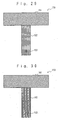
- the cantilever 162 contains whisker crystals arranged along a specific direction or in a specific pattern. That is, the cantilever 162 is mainly formed of plastic containing whisker crystals arranged along the axial direction of the cantilever.
- whisker crystals arranged along a specific direction or in a specific pattern are incorporated into the cantilever, it becomes possible to impart to the cantilever anisotropy in mechanical properties and electrical properties, which anisotropy cannot be obtained in a cantilever formed of a single material only.
- FIG. 31 is a configurational view of a nanometric mechanical oscillator according to a sixteenth embodiment of the present invention.
- a nanometric mechanical oscillator 170 of the present embodiment includes a base 171, a cantilever 174, and a probe 175 attached to the tip of the cantilever 174 (on the reverse side).
- the cantilever 174 is guided by guides 173.
- Two surface-acoustic-wave generation units 172 and 176 each serving as an actuator are disposed on the base 171.
- the cantilever 174 can be moved in order to change the effective length thereof.
- the distribution of material properties of a sample can be investigated on the basis of the manner of generation of higher order modes of oscillation of the cantilever.
- the length of the cantilever is fixed, measurement can be performed at discrete frequencies only.
- the oscillation frequency of the cantilever can be swept continuously or swept within a wide frequency range. As a result, more accurate measurement of sample characteristics becomes possible; and a small distribution of' material properties within a sample, which has been impossible to observe, can be visualized.
- FIG. 32 is a configurational view of a nanometric mechanical oscillator according to a seventeenth embodiment of the present invention.
- a nanometric mechanical oscillator 180 of the present embodiment includes a series of attraction electrodes 182, which are disposed to surround one end portion of a cantilever 183 disposed on a base 181.
- the attraction electrodes 182 selectively attract different portions of the cantilever 183 by means of electrostatic attraction force to thereby move the cantilever 183 and thus change the effective length of the cantilever 183.
- Reference numeral 184 denotes a probe; 185 denotes a guide; and 186 denotes a surface-acoustic-wave generation unit.
- the fundamental oscillation frequency and the higher order mode can be swept. Therefore, through fabrication of a surface-acoustic-wave generation element in the vicinity of the base end of the cantilever, it becomes possible to sweep the fundamental oscillation frequency and the higher order mode within a wide frequency band.
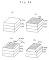
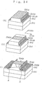
- FIGS. 33 to 36 are views showing steps of fabricating a nanometric mechanical oscillator according to an eighteenth embodiment of the present invention.
- Step (12) will be described in detail with reference to FIGS. 37 and 38.
- FIG. 39 is a view showing a cantilever array according to a nineteenth embodiment of the present invention in which an oscillator having a triangular-pyramidal probe is provided at the tip end of a chip.
- one oscillator 302 having a triangular-pyramidal probe can be disposed at the tip portion 301 of a millimetric chip which can be handled by use of, for example, tweezers.
- a large number of arrayed cantilevers 303 each having a triangular-pyramidal probe can be formed. Thus, one of the cantilevers 303 closest to the tip can be brought into contact with a sample.
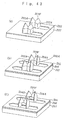
- FIGS. 40 to 43 are views showing steps of fabricating a nanometric mechanical oscillator according to a twentieth embodiment of the present invention.
- FIGS. 44 to 47 are views showing steps of fabricating a nanometric mechanical oscillator according to a twenty-first embodiment of the present invention.
- oblique vapor deposition is performed from opposite sides to form a parallel spring consisting of two plate springs, which support a probe mass or a mass having a flat plane.
- the present invention can greatly improve the resolution of a scanning force microscope in detecting variations in force or mass. That is, a probe having a stable nanometric mechanical oscillator can be fabricated.
- a scanning force microscope which uses, as a probe, an oscillator fabricated in the above-described manner can be realized.
- a single atom or a cluster of atoms are scanned, and a resultant variation in the characteristic frequency of the oscillator-type probe can be detected.
- the possibility of atom identification can be investigated.
- performance as an ordinary scanning force microscope can be evaluated.
- the present invention is suitable for application to a stable scanning force microscope of high sensitivity and is expected to be applied to mass spectrometers.
Landscapes
- Physics & Mathematics (AREA)
- General Physics & Mathematics (AREA)
- Radiology & Medical Imaging (AREA)
- Health & Medical Sciences (AREA)
- General Health & Medical Sciences (AREA)
- Nuclear Medicine, Radiotherapy & Molecular Imaging (AREA)
- Engineering & Computer Science (AREA)
- Power Engineering (AREA)
- Acoustics & Sound (AREA)
- Computer Hardware Design (AREA)
- Microelectronics & Electronic Packaging (AREA)
- Testing Or Measuring Of Semiconductors Or The Like (AREA)
- Micromachines (AREA)
- Length Measuring Devices With Unspecified Measuring Means (AREA)
- Investigating Strength Of Materials By Application Of Mechanical Stress (AREA)
- Investigating Or Analyzing Materials By The Use Of Ultrasonic Waves (AREA)
Abstract
Description
Claims (9)
- A measurement apparatus using a nanometric mechanical oscillator comprising:characterized in that the elastic neck portion is a micro thin wire shape whereby physical characteristics of a sample are measured by oscillation of the oscillator mass caused by the sample.(a) a base;(b) an oscillator mass; and(c) an elastic neck portion for connecting the base and the oscillator mass:
- A measurement apparatus according to Claim 1, wherein the micro thin wire shaped neck portion is formed of a nano tube or whisker, whereby interaction between the oscillator mass and the sample is detected to thereby obtain an image.
- A measurement apparatus according to Claim 1, characterized in that a core of an optical fiber is fixed to the nanometric mechanical oscillator such that the oscillator faces a sample; and oscillation of the oscillator mass caused by the sample is detected optically.
- A measurement apparatus according to Claim 1, characterized in that under vacuum, an electron beam from an electrode is radiated onto the oscillator, while being focused to have a focal point on the nanometer order; the base of the oscillator has electrical conductivity, and a portion of the oscillator exhibits a piezo effect; the oscillator causes self-excited oscillation due to current that flows upon irradiation with the electron beam and displacement of the oscillator caused by the current; and variation in current flowing out of the oscillator is detected by a high-frequency current detector to thereby detect the amplitude and frequency of the oscillation of the oscillator.
- A measurement apparatus according to Claim 1, characterized in that through use of a solid immersion lens, a spot of light focused to a degree beyond a bendable limit is formed in the vicinity of the base of the nanometric mechanical oscillator; and the amplitude and frequency of oscillation of the oscillator are detected on the basis of return light.
- A measurement apparatus according to Claim 1, characterized in that the oscillator is fixedly disposed on a layered substrate having a mask layer of Sb; a laser beam is radiated onto the mask layer so as to change a portion of the mask to thereby establish a state equal to formation of a nanometric opening; and thus oscillation of the oscillator only is detected.
- A measurement apparatus according to Claim 1, characterized in that the substrate is a piezo substrate and comb-shaped electrodes are disposed on the piezo substrate; and AC voltage is applied to the electrodes to thereby generate surface acoustic waves, which excite the oscillator to oscillate.
- A measurement apparatus according to Claim 1, comprising a nanometric mechanical oscillator having a plurality of oscillator masses on the base, characterized in that displacement of the oscillator masses which is caused upon collision of a particle with the oscillator in accordance with the law of conservation of momentum is measured so as to detect a velocity of the particle.
- A measurement apparatus according to Claim 1, characterized in that acceleration or force acted to the nanometric mechanical oscillator is measured.
Applications Claiming Priority (5)
| Application Number | Priority Date | Filing Date | Title |
|---|---|---|---|
| JP20268299 | 1999-07-16 | ||
| JP20268299 | 1999-07-16 | ||
| JP2000156645 | 2000-05-26 | ||
| JP2000156645A JP2001091441A (en) | 1999-07-16 | 2000-05-26 | Mechanical vibrator of nanometer order, method of manufacturing the same, and measuring device using the same |
| EP00944395A EP1203749B1 (en) | 1999-07-16 | 2000-07-11 | Nanometer-order mechanical vibrator, production method thereof and measuring device using it |
Related Parent Applications (1)
| Application Number | Title | Priority Date | Filing Date |
|---|---|---|---|
| EP00944395A Division EP1203749B1 (en) | 1999-07-16 | 2000-07-11 | Nanometer-order mechanical vibrator, production method thereof and measuring device using it |
Publications (2)
| Publication Number | Publication Date |
|---|---|
| EP1583104A2 true EP1583104A2 (en) | 2005-10-05 |
| EP1583104A3 EP1583104A3 (en) | 2007-04-04 |
Family
ID=26513524
Family Applications (7)
| Application Number | Title | Priority Date | Filing Date |
|---|---|---|---|
| EP05005157A Expired - Lifetime EP1553047B1 (en) | 1999-07-16 | 2000-07-11 | Nanometric mechanical oscillator |
| EP07000437A Withdrawn EP1775258A1 (en) | 1999-07-16 | 2000-07-11 | Nanometric mechanical oscillator, method of fabricating the same, and measurement apparatus using the same |
| EP05005160A Withdrawn EP1553048A1 (en) | 1999-07-16 | 2000-07-11 | Nanometric mechanical oscillator |
| EP07000436A Withdrawn EP1767490A3 (en) | 1999-07-16 | 2000-07-11 | Nanometric mechanical oscillator, method of fabricating the same, and measurement apparatus using the same |
| EP00944395A Expired - Lifetime EP1203749B1 (en) | 1999-07-16 | 2000-07-11 | Nanometer-order mechanical vibrator, production method thereof and measuring device using it |
| EP07003493A Withdrawn EP1780173A1 (en) | 1999-07-16 | 2000-07-11 | Nanometric mechanical oscillator, method of fabricating the same, and measurement apparatus using the same |
| EP05005173A Withdrawn EP1583104A3 (en) | 1999-07-16 | 2000-07-11 | Nanometric mechanical oscillator, method of fabricating the same, and measurement apparatus using the same |
Family Applications Before (6)
| Application Number | Title | Priority Date | Filing Date |
|---|---|---|---|
| EP05005157A Expired - Lifetime EP1553047B1 (en) | 1999-07-16 | 2000-07-11 | Nanometric mechanical oscillator |
| EP07000437A Withdrawn EP1775258A1 (en) | 1999-07-16 | 2000-07-11 | Nanometric mechanical oscillator, method of fabricating the same, and measurement apparatus using the same |
| EP05005160A Withdrawn EP1553048A1 (en) | 1999-07-16 | 2000-07-11 | Nanometric mechanical oscillator |
| EP07000436A Withdrawn EP1767490A3 (en) | 1999-07-16 | 2000-07-11 | Nanometric mechanical oscillator, method of fabricating the same, and measurement apparatus using the same |
| EP00944395A Expired - Lifetime EP1203749B1 (en) | 1999-07-16 | 2000-07-11 | Nanometer-order mechanical vibrator, production method thereof and measuring device using it |
| EP07003493A Withdrawn EP1780173A1 (en) | 1999-07-16 | 2000-07-11 | Nanometric mechanical oscillator, method of fabricating the same, and measurement apparatus using the same |
Country Status (6)
| Country | Link |
|---|---|
| US (1) | US6611178B1 (en) |
| EP (7) | EP1553047B1 (en) |
| JP (1) | JP2001091441A (en) |
| KR (1) | KR100501787B1 (en) |
| DE (2) | DE60034684T2 (en) |
| WO (1) | WO2001005701A1 (en) |
Families Citing this family (26)
| Publication number | Priority date | Publication date | Assignee | Title |
|---|---|---|---|---|
| FR2816407B1 (en) * | 2000-11-06 | 2003-03-28 | Centre Nat Rech Scient | APPARATUS FOR PARALLEL DETECTION OF THE BEHAVIOR OF MECHANICAL MICROOSCILLATORS |
| JP4076792B2 (en) | 2001-06-19 | 2008-04-16 | 独立行政法人科学技術振興機構 | Cantilever array, manufacturing method and apparatus |
| US6953930B2 (en) * | 2001-08-27 | 2005-10-11 | Nippon Telegraph And Telephone Corporation | Conductive transparent probe and probe control apparatus |
| JP2004058267A (en) * | 2002-06-03 | 2004-02-26 | Japan Science & Technology Corp | Three-dimensional structure made of silicon fine wire, method of manufacturing the same, and apparatus using the same |
| KR20060036456A (en) * | 2003-07-16 | 2006-04-28 | 도쿠리쓰교세이호징 가가쿠 기주쓰 신코 기코 | Scanning probe microscope probe and its manufacturing method |
| KR100793122B1 (en) * | 2003-08-11 | 2008-01-10 | 도쿠리쓰교세이호징 가가쿠 기주쓰 신코 기코 | Probe for probe microscope using transparent substrate, manufacturing method thereof and probe microscope device |
| JP4535706B2 (en) * | 2003-10-07 | 2010-09-01 | アオイ電子株式会社 | Cantilever for scanning probe microscope and manufacturing method thereof |
| US6812460B1 (en) * | 2003-10-07 | 2004-11-02 | Zyvex Corporation | Nano-manipulation by gyration |
| JP2006112788A (en) * | 2004-10-12 | 2006-04-27 | Canon Inc | Surface shape measuring apparatus, surface measuring method, and exposure apparatus |
| JP2006125984A (en) * | 2004-10-28 | 2006-05-18 | Japan Science & Technology Agency | Measuring device with daisy type cantilever wheel |
| JP4689363B2 (en) | 2005-06-20 | 2011-05-25 | 日産自動車株式会社 | Sound increaser |
| FR2889371A1 (en) * | 2005-07-29 | 2007-02-02 | Commissariat Energie Atomique | DEVICE FOR CONVERTING MECHANICAL ENERGY IN ELECTRIC ENERGY BY CYCLE OF ELECTRICAL LOADS AND DISCHARGES ON THE CONNECTORS OF A CAPACITOR |
| JP4559928B2 (en) * | 2005-08-11 | 2010-10-13 | セイコーインスツル株式会社 | Cantilever |
| US7629192B2 (en) * | 2005-10-13 | 2009-12-08 | International Business Machines Corporation | Passive electrically testable acceleration and voltage measurement devices |
| AT503995B1 (en) * | 2006-08-07 | 2009-03-15 | Arc Seibersdorf Res Gmbh | MINIATURE SENSOR ACCELERATION |
| KR100798361B1 (en) * | 2007-02-01 | 2008-01-28 | 포항공과대학교 산학협력단 | Micromass Sensors with Detector Columns |
| FR2915803B1 (en) * | 2007-05-02 | 2012-06-08 | Centre Nat Rech Scient | PROBE FOR ATOMIC FORCE MICROSCOPY |
| KR100922765B1 (en) * | 2007-05-18 | 2009-10-21 | 명지대학교 산학협력단 | Molecular detector |
| JP5035797B2 (en) * | 2007-07-25 | 2012-09-26 | 学校法人立命館 | Probe forming etching mask and probe manufacturing method using the same |
| KR100943707B1 (en) * | 2007-10-05 | 2010-02-23 | 한국전자통신연구원 | 3D Nano Devices Including Nanostructures |
| KR101027517B1 (en) * | 2007-11-23 | 2011-04-06 | 재단법인서울대학교산학협력재단 | Arrangement method of nano structures and manufacturing method of nano device using same |
| WO2009066968A2 (en) * | 2007-11-23 | 2009-05-28 | Seoul National University Industry Foundation | Method for arranging nanostructures and manufacturing nano devices using the same |
| GB2458906A (en) * | 2008-04-01 | 2009-10-07 | Sharp Kk | Nanowire manufacture |
| DE102009041547B4 (en) | 2009-09-15 | 2012-10-25 | Fraunhofer-Gesellschaft zur Förderung der angewandten Forschung e.V. | Device and method for activating a WLAN-capable device |
| FR3012255B1 (en) * | 2013-10-17 | 2017-03-10 | Commissariat Energie Atomique | PROCESS FOR FORMING WRINKLES BY FUSIONING A FOUNDATION ON WHICH RESTORATES A CONSTRAINED LAYER |
| EP4379397B1 (en) | 2022-11-30 | 2026-03-18 | Imec VZW | A method for producing a substrate comprising multiple tips for scanning probe microscopy |
Family Cites Families (11)
| Publication number | Priority date | Publication date | Assignee | Title |
|---|---|---|---|---|
| US5021364A (en) * | 1989-10-31 | 1991-06-04 | The Board Of Trustees Of The Leland Stanford Junior University | Microcantilever with integral self-aligned sharp tetrahedral tip |
| US5319977A (en) * | 1991-06-20 | 1994-06-14 | The Board Of Trustees Of The Leland Stanford Junior University | Near field acoustic ultrasonic microscope system and method |
| EP0530473B1 (en) * | 1991-07-15 | 1996-03-13 | Matsushita Electric Industrial Co., Ltd. | Cantilever for atomic force microscope and method of manufacturing the same |
| JP2549789B2 (en) | 1992-01-13 | 1996-10-30 | 日本電信電話株式会社 | Coordinated control method for multiple actuators |
| JP3081979B2 (en) * | 1992-05-08 | 2000-08-28 | セイコーインスツルメンツ株式会社 | microscope |
| JPH06305898A (en) * | 1993-03-10 | 1994-11-01 | Internatl Business Mach Corp <Ibm> | Single crystal tip structure and its formation |
| DE19701701A1 (en) * | 1997-01-21 | 1998-07-23 | Zeiss Carl Fa | Probe array for a scanning probe microscope |
| JPH10247118A (en) | 1997-03-03 | 1998-09-14 | Canon Inc | Micro-damper, and sensor, actuator, and probe having the micro-damper, and scanning probe microscope, processing apparatus, and information processing apparatus having the probe |
| JPH10300762A (en) | 1997-04-30 | 1998-11-13 | Hitachi Constr Mach Co Ltd | Cantilever manufacturing method |
| JPH11201848A (en) | 1998-01-08 | 1999-07-30 | Omron Corp | Capacitive sensor and detection method |
| US6441371B1 (en) * | 2000-04-03 | 2002-08-27 | Korea Institute Of Science And Technology | Scanning probe microscope |
-
2000
- 2000-05-26 JP JP2000156645A patent/JP2001091441A/en active Pending
- 2000-07-11 EP EP05005157A patent/EP1553047B1/en not_active Expired - Lifetime
- 2000-07-11 WO PCT/JP2000/004622 patent/WO2001005701A1/en not_active Ceased
- 2000-07-11 DE DE60034684T patent/DE60034684T2/en not_active Expired - Fee Related
- 2000-07-11 EP EP07000437A patent/EP1775258A1/en not_active Withdrawn
- 2000-07-11 KR KR10-2002-7000547A patent/KR100501787B1/en not_active Expired - Fee Related
- 2000-07-11 EP EP05005160A patent/EP1553048A1/en not_active Withdrawn
- 2000-07-11 EP EP07000436A patent/EP1767490A3/en not_active Withdrawn
- 2000-07-11 EP EP00944395A patent/EP1203749B1/en not_active Expired - Lifetime
- 2000-07-11 EP EP07003493A patent/EP1780173A1/en not_active Withdrawn
- 2000-07-11 DE DE60037765T patent/DE60037765T2/en not_active Expired - Fee Related
- 2000-07-11 EP EP05005173A patent/EP1583104A3/en not_active Withdrawn
- 2000-07-11 US US10/009,560 patent/US6611178B1/en not_active Expired - Fee Related
Also Published As
| Publication number | Publication date |
|---|---|
| US6611178B1 (en) | 2003-08-26 |
| EP1767490A3 (en) | 2007-07-04 |
| EP1553048A1 (en) | 2005-07-13 |
| EP1775258A1 (en) | 2007-04-18 |
| EP1553047A1 (en) | 2005-07-13 |
| EP1203749A4 (en) | 2002-09-25 |
| DE60037765T2 (en) | 2008-06-05 |
| WO2001005701A1 (en) | 2001-01-25 |
| DE60037765D1 (en) | 2008-02-21 |
| DE60034684D1 (en) | 2007-06-14 |
| EP1767490A2 (en) | 2007-03-28 |
| KR20020035836A (en) | 2002-05-15 |
| EP1583104A3 (en) | 2007-04-04 |
| EP1203749B1 (en) | 2007-05-02 |
| KR100501787B1 (en) | 2005-07-18 |
| DE60034684T2 (en) | 2008-01-17 |
| EP1203749A1 (en) | 2002-05-08 |
| EP1553047B1 (en) | 2008-01-09 |
| EP1780173A1 (en) | 2007-05-02 |
| JP2001091441A (en) | 2001-04-06 |
Similar Documents
| Publication | Publication Date | Title |
|---|---|---|
| EP1203749B1 (en) | Nanometer-order mechanical vibrator, production method thereof and measuring device using it | |
| US5354985A (en) | Near field scanning optical and force microscope including cantilever and optical waveguide | |
| JP2709240B2 (en) | How to perform acoustic microscopy | |
| WO1997034122A1 (en) | Cantilever structures | |
| US10527645B2 (en) | Compact probe for atomic-force microscopy and atomic-force microscope including such a probe | |
| IL173090A (en) | Probe for an atomic force microscope | |
| Minh et al. | High throughput aperture near-field scanning optical microscopy | |
| JP2010526284A (en) | Probe for atomic force microscopy | |
| US6415653B1 (en) | Cantilever for use in a scanning probe microscope | |
| JP2002310883A (en) | Cantilever for scanning probe microscope | |
| JPH04369418A (en) | Cantilever probes, atomic force microscopes, information recording and reproducing devices | |
| US7278297B2 (en) | Oscillating probe with a virtual probe tip | |
| Yamada et al. | Scanning near‐field optical microscopy using piezoelectric cantilevers | |
| US10302673B2 (en) | Miniaturized and compact probe for atomic force microscopy | |
| JP2006153886A (en) | Nanometer mechanical vibrator, manufacturing method thereof, and measuring apparatus using the same | |
| US20030230709A1 (en) | Probe, near-field light generation apparatus including probe, exposure apparatus, and exposing method using probe | |
| EP1130379B1 (en) | Optical cantilever for scanning microscope and method of its production | |
| US7861315B2 (en) | Method for microfabricating a probe with integrated handle, cantilever, tip and circuit | |
| JP4751190B2 (en) | Probe for temperature measurement | |
| US20240118310A1 (en) | Device for measuring and/or modifying a surface | |
| JPH11230974A (en) | Probe and method for producing the same | |
| JPH1138020A (en) | Scanning probe microscopy, scanning probe microscope probes and scanning probe microscopes | |
| Schumaker et al. | Ultrasonic force microscopic characterization of nanosized copper particles | |
| JP2007192589A (en) | Probe for temperature measurement | |
| Van Den Bos et al. | A new concept in magnetic force microscope cantilevers |
Legal Events
| Date | Code | Title | Description |
|---|---|---|---|
| PUAI | Public reference made under article 153(3) epc to a published international application that has entered the european phase |
Free format text: ORIGINAL CODE: 0009012 |
|
| AC | Divisional application: reference to earlier application |
Ref document number: 1203749 Country of ref document: EP Kind code of ref document: P |
|
| AK | Designated contracting states |
Kind code of ref document: A2 Designated state(s): CH DE FR GB LI |
|
| RIN1 | Information on inventor provided before grant (corrected) |
Inventor name: KAWAKATSU, HIDEKI Inventor name: TOSHIYOSHI, HIROSHI |
|
| PUAL | Search report despatched |
Free format text: ORIGINAL CODE: 0009013 |
|
| AK | Designated contracting states |
Kind code of ref document: A3 Designated state(s): CH DE FR GB LI |
|
| RIC1 | Information provided on ipc code assigned before grant |
Ipc: G01P 15/00 20060101ALI20070223BHEP Ipc: G01N 13/16 20060101ALI20070223BHEP Ipc: G12B 21/20 20060101ALI20070223BHEP Ipc: H01L 29/84 20060101ALI20070223BHEP Ipc: G11B 9/14 20060101ALI20070223BHEP Ipc: B81C 1/00 20060101ALI20070223BHEP Ipc: G12B 21/02 20060101ALI20070223BHEP Ipc: B81B 3/00 20060101AFI20070223BHEP |
|
| 17P | Request for examination filed |
Effective date: 20070413 |
|
| AKX | Designation fees paid |
Designated state(s): CH DE FR GB LI |
|
| STAA | Information on the status of an ep patent application or granted ep patent |
Free format text: STATUS: THE APPLICATION HAS BEEN WITHDRAWN |
|
| 18W | Application withdrawn |
Effective date: 20080314 |