EP1582359A2 - Thermal head having adhesive layer partially disposed on heat sink and method for manufacturing such thermal head - Google Patents
Thermal head having adhesive layer partially disposed on heat sink and method for manufacturing such thermal head Download PDFInfo
- Publication number
- EP1582359A2 EP1582359A2 EP05005486A EP05005486A EP1582359A2 EP 1582359 A2 EP1582359 A2 EP 1582359A2 EP 05005486 A EP05005486 A EP 05005486A EP 05005486 A EP05005486 A EP 05005486A EP 1582359 A2 EP1582359 A2 EP 1582359A2
- Authority
- EP
- European Patent Office
- Prior art keywords
- printed
- circuit board
- head substrate
- heat sink
- wire
- Prior art date
- Legal status (The legal status is an assumption and is not a legal conclusion. Google has not performed a legal analysis and makes no representation as to the accuracy of the status listed.)
- Withdrawn
Links
- 239000012790 adhesive layer Substances 0.000 title claims abstract description 38
- 238000000034 method Methods 0.000 title claims description 13
- 238000004519 manufacturing process Methods 0.000 title claims description 8
- 239000000758 substrate Substances 0.000 claims abstract description 110
- 229920005989 resin Polymers 0.000 claims abstract description 29
- 239000011347 resin Substances 0.000 claims abstract description 29
- 230000005611 electricity Effects 0.000 claims abstract description 14
- 239000000853 adhesive Substances 0.000 claims description 25
- 230000001070 adhesive effect Effects 0.000 claims description 25
- 239000000463 material Substances 0.000 claims description 18
- 238000007789 sealing Methods 0.000 claims description 16
- 238000003892 spreading Methods 0.000 claims description 2
- 229910052782 aluminium Inorganic materials 0.000 description 23
- XAGFODPZIPBFFR-UHFFFAOYSA-N aluminium Chemical compound [Al] XAGFODPZIPBFFR-UHFFFAOYSA-N 0.000 description 22
- 239000010410 layer Substances 0.000 description 14
- XUIMIQQOPSSXEZ-UHFFFAOYSA-N Silicon Chemical compound [Si] XUIMIQQOPSSXEZ-UHFFFAOYSA-N 0.000 description 4
- 239000010703 silicon Substances 0.000 description 4
- 229910052710 silicon Inorganic materials 0.000 description 4
- 239000003822 epoxy resin Substances 0.000 description 3
- 229920000647 polyepoxide Polymers 0.000 description 3
- 238000005452 bending Methods 0.000 description 2
- 230000007423 decrease Effects 0.000 description 2
- 238000005549 size reduction Methods 0.000 description 2
- 239000000956 alloy Substances 0.000 description 1
- 229910045601 alloy Inorganic materials 0.000 description 1
- PNEYBMLMFCGWSK-UHFFFAOYSA-N aluminium oxide Inorganic materials [O-2].[O-2].[O-2].[Al+3].[Al+3] PNEYBMLMFCGWSK-UHFFFAOYSA-N 0.000 description 1
- 230000015572 biosynthetic process Effects 0.000 description 1
- 229910010293 ceramic material Inorganic materials 0.000 description 1
Images

Classifications
-
- B—PERFORMING OPERATIONS; TRANSPORTING
- B41—PRINTING; LINING MACHINES; TYPEWRITERS; STAMPS
- B41J—TYPEWRITERS; SELECTIVE PRINTING MECHANISMS, i.e. MECHANISMS PRINTING OTHERWISE THAN FROM A FORME; CORRECTION OF TYPOGRAPHICAL ERRORS
- B41J2/00—Typewriters or selective printing mechanisms characterised by the printing or marking process for which they are designed
- B41J2/315—Typewriters or selective printing mechanisms characterised by the printing or marking process for which they are designed characterised by selective application of heat to a heat sensitive printing or impression-transfer material
- B41J2/32—Typewriters or selective printing mechanisms characterised by the printing or marking process for which they are designed characterised by selective application of heat to a heat sensitive printing or impression-transfer material using thermal heads
- B41J2/335—Structure of thermal heads
-
- H—ELECTRICITY
- H05—ELECTRIC TECHNIQUES NOT OTHERWISE PROVIDED FOR
- H05K—PRINTED CIRCUITS; CASINGS OR CONSTRUCTIONAL DETAILS OF ELECTRIC APPARATUS; MANUFACTURE OF ASSEMBLAGES OF ELECTRICAL COMPONENTS
- H05K3/00—Apparatus or processes for manufacturing printed circuits
- H05K3/0058—Laminating printed circuit boards onto other substrates, e.g. metallic substrates
-
- H—ELECTRICITY
- H05—ELECTRIC TECHNIQUES NOT OTHERWISE PROVIDED FOR
- H05K—PRINTED CIRCUITS; CASINGS OR CONSTRUCTIONAL DETAILS OF ELECTRIC APPARATUS; MANUFACTURE OF ASSEMBLAGES OF ELECTRICAL COMPONENTS
- H05K3/00—Apparatus or processes for manufacturing printed circuits
- H05K3/38—Improvement of the adhesion between the insulating substrate and the metal
- H05K3/386—Improvement of the adhesion between the insulating substrate and the metal by the use of an organic polymeric bonding layer, e.g. adhesive
Definitions
- the present invention relates to thermal heads installed in, for example, thermal-transfer printers, and to methods for manufacturing such thermal heads.
- a typical thermal head is provided with a plurality of exothermic bodies which generate heat when electricity is applied thereto.
- the thermal energy generated by the exothermic bodies is supplied to a recording medium in order to perform a recording operation.
- a thermal head is provided with a head substrate and a printed-circuit board, which are attached on an aluminum heat-sink.
- the head substrate includes the plurality of exothermic bodies, a common electrode connected with first ends of the exothermic bodies, and a plurality of independent electrodes connected with corresponding second ends of the exothermic bodies.
- the printed-circuit board includes a plurality of driving elements for controlling the electricity supplied to the exothermic bodies via the independent electrodes of the head substrate.
- the head substrate and the printed-circuit board are disposed on the aluminum heat-sink in a manner such that an end-surface of the head substrate and an end-surface of the printed-circuit board adjoin each other.
- the independent electrodes of the head substrate and the driving elements of the printed-circuit board are correspondingly wire-connected with each other across a bordering section between the head substrate and the printed-circuit board so as to form a wire-connection unit.
- Such a wire-connection unit is sealed with a sealing-resin material, such as epoxy resin, whose viscosity decreases when heat is applied thereto.
- the sealing-resin material covers the wire-connection unit without leaving any empty spaces.
- the heated sealing-resin material in a low viscosity state moves further past the gap between the head substrate and the printed-circuit board to enter the groove in the heat sink, and as a result, the sealing-resin material adheres to an elastic adhesive provided for an attachment between the head substrate and the heat sink. If the sealing-resin material adheres to the elastic adhesive, the head substrate and the heat sink become tightly combined with each other. This increases the rigidity between the head substrate and the heat sink, or in other words, reduces the elasticity between the two. In this case, even when the sealing-resin material hardens while the heat sink is thermally expanded, the elastic adhesive cannot absorb such thermal expansion of the heat sink. This forces the top and bottom surfaces of the head substrate to warp significantly. In order to increase the yielding rate, it is preferred that the head substrate is kept flat as much as possible.
- the present invention is characterized in that an adhesive layer provided for an attachment between a printed-circuit board and a heat sink is only partially disposed therebetween such that a space is provided below an end-surface of a head substrate and an end-surface of the printed-circuit board adjoining each other. This space connects a gap formed between the adjoining end-surfaces with the outside of the thermal head.
- the present invention provides a thermal head which includes a head substrate including a plurality of exothermic bodies which generate heat when electricity is supplied thereto, a common electrode connected with first ends of the exothermic bodies, and a plurality of independent electrodes connected with corresponding second ends of the exothermic bodies; a printed-circuit board including a plurality of driving elements for controlling the electricity supplied to the exothermic bodies on the head substrate; and a heat sink on which the head substrate and the printed-circuit board are attached in a manner such that an end-surface of the head substrate and an end-surface of the printed-circuit board adjoin each other.
- the plurality of independent electrodes and the plurality of driving elements are correspondingly wire-connected with each other across a gap formed between the adjoining end-surfaces of the head substrate and the printed-circuit board so as to define a wire-connection unit.
- the wire-connection unit is sealed with a resin material.
- the printed-circuit board and the heat sink have an adhesive layer partially disposed therebetween such that a space is provided between the printed-circuit board and the heat sink, the space communicating with the outside of the thermal head and with the gap between the adjoining end-surfaces of the head substrate and the printed-circuit board.
- the space is preferably disposed below the adjoining end-surfaces of the head substrate and the printed-circuit board, and is preferably symmetrical in plan view with respect to a line perpendicular to a direction in which the adjoining end-surfaces extend.
- the symmetrical space allows the adhesive layer partially disposed between the printed-circuit board and the heat sink to contract more evenly when the adhesive layer hardens.
- the printed-circuit board can be attached horizontally on the heat sink in a well-balanced manner.
- the adhesive layer preferably has a central portion and two side portions in plan view with respect to a direction in which the adjoining end-surfaces extend, the central portion extending longer than the side portions in a direction perpendicular to the direction in which the adjoining end-surfaces extend.
- attachment surfaces among the heat sink, the head substrate, and the printed-circuit board are preferably flat.
- the present invention also provides a method for fabricating a thermal head which includes a head substrate including a plurality of exothermic bodies which generate heat when electricity is supplied thereto, a common electrode connected with first ends of the exothermic bodies, and a plurality of independent electrodes connected with corresponding second ends of the exothermic bodies; a printed-circuit board including a plurality of driving elements for controlling the electricity supplied to the exothermic bodies on the head substrate; and a heat sink on which the head substrate and the printed-circuit board are attached in a manner such that an end-surface of the head substrate and an end-surface of the printed-circuit board adjoin each other.
- the plurality of independent electrodes and the plurality of driving elements are correspondingly wire-connected with each other across a gap formed between the adjoining end-surfaces of the head substrate and the printed-circuit board so as to define a wire-connection unit.
- the wire-connection unit is sealed with a resin material.
- the printed-circuit board and the heat sink have an adhesive layer partially disposed therebetween such that a space is provided between the printed-circuit board and the heat sink, the space communicating with the outside of the thermal head and with the gap between the adjoining end-surfaces of the head substrate and the printed-circuit board.
- the method preferably includes the following steps of attaching the head substrate onto the heat sink; applying a first adhesive onto the heat sink in a direction parallel to the end-surface of the head substrate to be adjoining the printed-circuit board at a substantially uniform width; applying a second adhesive to a central portion of the first adhesive such that the second adhesive forms a substantially circular shape in plan view; spreading the first adhesive and the second adhesive towards the head substrate so as to form an adhesive layer having a central portion and two side portions in plan view with respect to a direction in which the end-surface of the head substrate to be adjoining the printed-circuit board extend, the central portion extending longer than the side portions in a direction perpendicular to the direction in which the end-surface of the head substrate extend; and attaching the printed-circuit board onto the heat sink via the adhesive layer in a manner such that the end-surface of the printed-circuit board and the end-surface of the head substrate adjoin each other.
- the method described above may further include the steps of wire-connecting the plurality of independent electrodes in the head substrate with the plurality of driving elements in the printed-circuit board so as to form the wire-connection unit; and sealing the wire-connection unit. Accordingly, even if the attachment surface area of the head substrate is reduced due to a size reduction of the head substrate, the tolerance level against the bending of the head substrate can be increased since the head substrate is preliminarily attached to the heat sink. This prevents the head substrate from warping caused by the thermal expansion of the heat sink.
- the present invention provides a thermal head and a method for manufacturing such a thermal head that prevent air holes from being formed in a sealing portion and that inhibit warping of a substrate caused by thermal expansion.
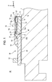
- Fig. 1 is a cross-sectional view illustrating a thermal head H1 according to a first embodiment of the present invention.
- the thermal head H1 includes a head substrate 10 shown in Fig. 2 and a printed-circuit board 30, which are attached on an aluminum heat-sink 1.
- the head substrate 10 and the printed-circuit board 30 are disposed on a top surface 1a of the aluminum heat-sink 1 such that end surfaces 10a and 30a of the respective head substrate 10 and the printed-circuit board 30 face and adjoin each other.
- the adjoining end-surfaces 10a and 30a of the respective head substrate 10 and printed-circuit board 30 actually have a gap 40 therebetween.
- the gap 40 in Fig. 1 is given a relatively large dimension for better viewability purposes, the actual gap 40 is significantly small.
- the head substrate 10 includes a base plate 11 composed of an alumina material or a ceramic material; a glazed layer 12 disposed over the base plate 11 and provided with a protruding portion adjacent to a first end of the head substrate 10 and a flat portion having a uniform thickness and extending from the protruding portion towards a second end of the head substrate 10; a plurality of exothermic bodies 13 disposed on the protruding portion of the glazed layer 12; a plurality of insulating-barrier-film components 14 each covering one of the exothermic bodies 13 and defining the planar dimension (resistance length L, resistance width W) of the corresponding exothermic body 13; an electrode layer 15 for transmitting electricity to the exothermic bodies 13; and a wear-resistant protection layer 17 for preventing the insulating-barrier-film components 14 and the electrode layer 15 from being in contact with, for example, a platen.
- a base plate 11 composed of an alumina material or a ceramic material
- a glazed layer 12
- the exothermic bodies 13 are segments of a resistance layer 13' disposed over the glazed layer 12 and are arranged at a predetermined interval in the y-axis direction shown in the drawings.
- the electrode layer 15 is formed entirely over the resistance layer 13' and the insulating-barrier-film components 14, and subsequently, openings 15c are formed in the electrode layer 15 so that the top surfaces of the insulating-barrier-film components 14 are exposed through these openings 15c. Consequently, the openings 15c separate the electrode layer 15 into a common electrode 15a and a plurality of independent electrodes 15b.
- the single common electrode 15a is connected with first ends of all of the exothermic bodies 13, whereas the independent electrodes 15b are connected with corresponding second ends of the exothermic bodies 13.
- Each of the independent electrodes 15b is provided with an electrode pad 16 for wire-connection.
- the electrode layer 15 and the electrode pads 16 in the first embodiment are composed of, for example, Al.
- the head substrate 10 is attached on the aluminum heat-sink 1 via an adhesive layer 23 having elasticity and absorbability for thermal-strain compensation.
- the printed-circuit board 30 is provided independently of the head substrate 10, and includes, for example, a plurality of driving elements 31 for controlling the electricity supplied to the exothermic bodies 13; and a connector 32 for connecting a circuit unit on the printed-circuit board 30, which includes the driving elements 31, with an external unit.
- the number of the driving elements 31 provided corresponds to the number of the exothermic bodies 13, and the driving elements 31 are arranged adjacent to a side of the printed-circuit board 30 adjoining the head substrate 10.
- the driving elements 31 are connected with the corresponding electrode pads 16 of the independent electrodes 15b in the head substrate 10 via corresponding Au connection wires 33, which are bridged over the gap 40 between the head substrate 10 and the printed-circuit board 30.
- the independent electrodes 15b, the electrode pads 16, the electrodes of the driving elements 31, and the Au connection wires 33 define a wire-connection unit.
- Such a wire-connection unit is sealed with sealing resin 34, such as epoxy resin.
- the sealing resin 34 also partially seals the gap 40 between the head substrate 10 and the printed-circuit board 30 such that the upper portion of the gap 40 is blocked.
- the electrodes of the driving elements 31 are also connected with the circuit unit on the printed-circuit board 30 via the Au connection wires 33.
- the printed-circuit board 30 and the aluminum heat-sink 1 have a space ⁇ and an adhesive layer 20 disposed therebetween.
- the space ⁇ communicates with the outside of the thermal head H1
- the adhesive layer 20 is disposed only partially between the printed-circuit board 30 and the aluminum heat-sink 1 in order to allow the space ⁇ to communicate with the gap 40 between the head substrate 10 and the printed-circuit board 30.
- the attachment surfaces of the printed-circuit board 30 and the aluminum heat-sink 1 are flat without any unevenness from a macroscopic viewpoint, such that the occupied area and the thickness of the adhesive layer 20 define the dimension of the space ⁇ .
- the adhesive layer 20 is substantially pentagonal in plan view, such that the adhesive layer 20 includes a central portion C and two side portions with respect to the direction in which the adjoining end-surfaces 10a and 30a of the respective head substrate 10 and printed-circuit board 30 extend, i.e. the y-axis direction.
- the central portion C extends longer than the side portions in a direction perpendicular to the adjoining end-surfaces 10a and 30a, i.e. the x-axis direction.
- the adhesive layer 20 is symmetrical with respect to the central portion C. Consequently, a space between the printed-circuit board 30 and the aluminum heat-sink 1 and where the adhesive layer 20 is not present defines the space ⁇ .
- the space ⁇ is thus provided below the adjoining end-surfaces 10a and 30a of the respective head substrate 10 and printed-circuit board 30, and has two parts which are symmetrical to each other with respect to a line perpendicular to the direction in which the adjoining end-surfaces 10a and 30a extend. Furthermore, the dimension of the space ⁇ is at minimum at the central portion C, and increases gradually from the central portion C towards the two side portions.
- the two parts of the space ⁇ communicate with the outside of the thermal head H1.
- the space ⁇ allows the gap 40 and the outside of the thermal head H1 to communicate with each other, and thus serves as air-vent passageways.
- the head substrate 10, the printed-circuit board 30, and the aluminum heat-sink 1 shown in Fig. 1 are prepared.
- the adhesive layer 23 is coated over a first area of the top surface 1a of the aluminum heat-sink 1 to which the head substrate 10 is to be attached.
- the head substrate 10 is then attached onto this first area via the adhesive layer 23.
- the head substrate 10 is attached in a manner such that the end-surface 10a having the plurality of independent electrodes 15b arranged adjacent thereto is placed adjacent to a second area of the top surface 1a of the aluminum heat-sink 1 to which the printed-circuit board 30 is to be attached.
- the adhesive layer 23 is composed of, for example, a silicon resin material having elasticity and absorbability that can compensate for thermal expansion of the aluminum heat-sink 1.
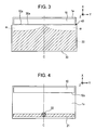
- a first adhesive 21 is applied partially onto the second area on the top surface 1a of the aluminum heat-sink 1. Specifically, the first adhesive 21 is applied in a direction parallel to the end-surface 10a of the head substrate 10 to be adjoining the printed-circuit board 30, i.e. the y-axis direction, at a substantially uniform width.
- a second adhesive 22 is applied onto a central portion of the first adhesive 21 such that the second adhesive 22 forms a substantially circular shape in plan view.
- the first adhesive 21 and the second adhesive 22 are then spread towards the head substrate 10, that is, in the x-axis direction, so as to form the adhesive layer 20 shown in Fig. 3.
- the adhesive layer 20 has the central portion C extending longer than the side portions in the x-axis direction, and is only partially formed in the area near where the end-surface 30a of the printed-circuit board 30 to be adjoining the head substrate 10 is to be disposed.
- the first adhesive 21 and the second adhesive 22 are composed of, for example, a silicon resin material.
- the printed-circuit board 30 is attached onto the aluminum heat-sink 1 via the adhesive layer 20 in a manner such that the end-surface 10a of the head substrate 10 and the end-surface 30a of the printed-circuit board 30 adjoin each other.
- the adhesive layer 20 is not present in the areas below the end-surface 30a of the printed-circuit board 30 where the space ⁇ for communicating with the outside of the thermal head H1 is formed. Since it is actually difficult to make the end-surface 30a of the printed-circuit board 30 exactly flat, a significantly small gap 40 is formed between the end-surface 10a and the end-surface 30a of the respective head substrate 10 and printed-circuit board 30.
- the space ⁇ communicates with the gap 40 formed between the printed-circuit board 30 and the head substrate 10.
- the electrode pads 16 of the independent electrodes 15b on the head substrate 10 are wire-connected to the corresponding driving elements 31 on the printed-circuit board 30 via the corresponding Au connection wires 33, which are bridged over the gap 40.
- a supersonic vibration is applied to the surface of the electrode pad 16 of each independent electrode 15b in order to destroy the oxidized film on the electrode pad 16.
- each electrode pad 16 is coated with an alloy layer of Al and Au, and is then connected to the corresponding Au connection wire 33.
- electrode pads disposed on the driving elements 31, which are not shown in the drawings are connected to the corresponding Au connection wires 33.
- the wire-connection unit including the electrode pads 16, the independent electrodes 15b, the driving elements 31 and so on connected with one another via the Au connection wires 33 is, for example, coated and sealed with the sealing resin 34 composed of a resin material, such as epoxy resin and silicon resin, whose viscosity decreases when heat is applied thereto.
- the heated sealing resin 34 in a low viscosity state covers the wire-connection unit without leaving any empty spaces, and also enters the gap 40 between the head substrate 10 and the printed-circuit board 30 so as to fill the upper portion of the gap 40.
- the air trapped in the gap 40 is forced to travel towards the space ⁇ communicating with the gap 40, and is then released from the space ⁇ towards the outside of the thermal head H1. This prevents air bubbles, caused by the air trapped inside the gap 40, from being formed in the sealing resin 34. Consequently, this allows the sealing resin 34 to completely seal the wire-connection unit without forming any air holes or uneven surfaces.
- the thermal head H1 shown in Fig. 1 is obtained.
- the sealing resin 34 entering the gap 40 can possibly protrude deeper into the gap 40, the possibility of the sealing resin 34 reaching the adhesive layers 20 and 23 via the space ⁇ is low since the gap 40 communicates with the space ⁇ not having the adhesive layers 20 and 23 present therein. Consequently, the adhesive layer 20 intervening between the aluminum heat-sink 1 and the printed-circuit board 30, and the adhesive layer 23 intervening between the aluminum heat-sink 1 and the head substrate 10 are capable of maintaining elasticity and absorbability to compensate for thermal expansion of the aluminum heat-sink 1. Thus, even when the sealing resin 34 hardens while the aluminum heat-sink 1 is thermally expanded, the elasticity of the adhesive layers 20 and 23 inhibits the warping of the head substrate 10 and the printed-circuit board 30.
- the head substrate 10 and the printed-circuit board 30 are preliminarily attached to the aluminum heat-sink 1 prior to the wire-connecting step and the sealing step, the head substrate 10 and the printed-circuit board 30 are advantageously made less bendable due to the adhesive layers 20 and 23.
- the sealing resin 34 hardens while the aluminum heat-sink 1 is thermally expanded, the head substrate 10 and the printed-circuit board 30 are effectively prevented from warping. This is especially effective when the surface area of the head substrate 10 is reduced in proportion to the size reduction of the thermal head H1 since in that case, the tolerance level against the bending of the head substrate 10 becomes lower.
- the head substrate 10 in the above embodiments is a true-glaze type
- the present invention can alternatively be applied to a thermal head provided with a head substrate of a partial-glaze type or a flat-glaze type, or a thermal head provided with a silicon head substrate.
Landscapes
- Electronic Switches (AREA)
Abstract
Description
- The present invention relates to thermal heads installed in, for example, thermal-transfer printers, and to methods for manufacturing such thermal heads.
- A typical thermal head is provided with a plurality of exothermic bodies which generate heat when electricity is applied thereto. The thermal energy generated by the exothermic bodies is supplied to a recording medium in order to perform a recording operation. Conventionally, a thermal head is provided with a head substrate and a printed-circuit board, which are attached on an aluminum heat-sink. The head substrate includes the plurality of exothermic bodies, a common electrode connected with first ends of the exothermic bodies, and a plurality of independent electrodes connected with corresponding second ends of the exothermic bodies. On the other hand, the printed-circuit board includes a plurality of driving elements for controlling the electricity supplied to the exothermic bodies via the independent electrodes of the head substrate. The head substrate and the printed-circuit board are disposed on the aluminum heat-sink in a manner such that an end-surface of the head substrate and an end-surface of the printed-circuit board adjoin each other. The independent electrodes of the head substrate and the driving elements of the printed-circuit board are correspondingly wire-connected with each other across a bordering section between the head substrate and the printed-circuit board so as to form a wire-connection unit. Such a wire-connection unit is sealed with a sealing-resin material, such as epoxy resin, whose viscosity decreases when heat is applied thereto. The sealing-resin material covers the wire-connection unit without leaving any empty spaces.
- In the thermal head having the structure described above, it is actually difficult to make the end-surface of the printed-circuit board adjoining the head substrate exactly flat, and due to this reason, a significantly small gap is formed between the head substrate and the printed-circuit board. When a heated sealing-resin material in a low viscosity state enters the gap between the head substrate and the printed-circuit board, the sealing-resin material traps air inside the gap, causing the air to expand. As a result, air bubbles are formed in the sealing-resin material. The formation of such air bubbles can lead to problems such as uneven surfaces or air holes formed in the hardened sealing-resin material. To prevent such problems, Japanese Unexamined Patent Application Publication No. 7-323592, for example, discloses a structure in which a section of the heat sink below the sealing portion in the gap between the head substrate and the printed-circuit board is provided with a groove through which the air can be released outward.
- However, according to such a heat sink provided with a groove, it has been discovered that the heated sealing-resin material in a low viscosity state moves further past the gap between the head substrate and the printed-circuit board to enter the groove in the heat sink, and as a result, the sealing-resin material adheres to an elastic adhesive provided for an attachment between the head substrate and the heat sink. If the sealing-resin material adheres to the elastic adhesive, the head substrate and the heat sink become tightly combined with each other. This increases the rigidity between the head substrate and the heat sink, or in other words, reduces the elasticity between the two. In this case, even when the sealing-resin material hardens while the heat sink is thermally expanded, the elastic adhesive cannot absorb such thermal expansion of the heat sink. This forces the top and bottom surfaces of the head substrate to warp significantly. In order to increase the yielding rate, it is preferred that the head substrate is kept flat as much as possible.
- Accordingly, it is an object of the present invention to provide a thermal head that prevents air holes from being formed in a sealing portion and that inhibits warping of a substrate caused by thermal expansion, and to provide a method for manufacturing such a thermal head.
- The present invention is characterized in that an adhesive layer provided for an attachment between a printed-circuit board and a heat sink is only partially disposed therebetween such that a space is provided below an end-surface of a head substrate and an end-surface of the printed-circuit board adjoining each other. This space connects a gap formed between the adjoining end-surfaces with the outside of the thermal head.
- Specifically, the present invention provides a thermal head which includes a head substrate including a plurality of exothermic bodies which generate heat when electricity is supplied thereto, a common electrode connected with first ends of the exothermic bodies, and a plurality of independent electrodes connected with corresponding second ends of the exothermic bodies; a printed-circuit board including a plurality of driving elements for controlling the electricity supplied to the exothermic bodies on the head substrate; and a heat sink on which the head substrate and the printed-circuit board are attached in a manner such that an end-surface of the head substrate and an end-surface of the printed-circuit board adjoin each other. The plurality of independent electrodes and the plurality of driving elements are correspondingly wire-connected with each other across a gap formed between the adjoining end-surfaces of the head substrate and the printed-circuit board so as to define a wire-connection unit. The wire-connection unit is sealed with a resin material. The printed-circuit board and the heat sink have an adhesive layer partially disposed therebetween such that a space is provided between the printed-circuit board and the heat sink, the space communicating with the outside of the thermal head and with the gap between the adjoining end-surfaces of the head substrate and the printed-circuit board.
- The space is preferably disposed below the adjoining end-surfaces of the head substrate and the printed-circuit board, and is preferably symmetrical in plan view with respect to a line perpendicular to a direction in which the adjoining end-surfaces extend. The symmetrical space allows the adhesive layer partially disposed between the printed-circuit board and the heat sink to contract more evenly when the adhesive layer hardens. Thus, the printed-circuit board can be attached horizontally on the heat sink in a well-balanced manner. In order to make the space symmetrical, the adhesive layer preferably has a central portion and two side portions in plan view with respect to a direction in which the adjoining end-surfaces extend, the central portion extending longer than the side portions in a direction perpendicular to the direction in which the adjoining end-surfaces extend.
- Furthermore, attachment surfaces among the heat sink, the head substrate, and the printed-circuit board are preferably flat.
- Furthermore, the present invention also provides a method for fabricating a thermal head which includes a head substrate including a plurality of exothermic bodies which generate heat when electricity is supplied thereto, a common electrode connected with first ends of the exothermic bodies, and a plurality of independent electrodes connected with corresponding second ends of the exothermic bodies; a printed-circuit board including a plurality of driving elements for controlling the electricity supplied to the exothermic bodies on the head substrate; and a heat sink on which the head substrate and the printed-circuit board are attached in a manner such that an end-surface of the head substrate and an end-surface of the printed-circuit board adjoin each other. The plurality of independent electrodes and the plurality of driving elements are correspondingly wire-connected with each other across a gap formed between the adjoining end-surfaces of the head substrate and the printed-circuit board so as to define a wire-connection unit. The wire-connection unit is sealed with a resin material. The printed-circuit board and the heat sink have an adhesive layer partially disposed therebetween such that a space is provided between the printed-circuit board and the heat sink, the space communicating with the outside of the thermal head and with the gap between the adjoining end-surfaces of the head substrate and the printed-circuit board.
- In detail, the method preferably includes the following steps of attaching the head substrate onto the heat sink; applying a first adhesive onto the heat sink in a direction parallel to the end-surface of the head substrate to be adjoining the printed-circuit board at a substantially uniform width; applying a second adhesive to a central portion of the first adhesive such that the second adhesive forms a substantially circular shape in plan view; spreading the first adhesive and the second adhesive towards the head substrate so as to form an adhesive layer having a central portion and two side portions in plan view with respect to a direction in which the end-surface of the head substrate to be adjoining the printed-circuit board extend, the central portion extending longer than the side portions in a direction perpendicular to the direction in which the end-surface of the head substrate extend; and attaching the printed-circuit board onto the heat sink via the adhesive layer in a manner such that the end-surface of the printed-circuit board and the end-surface of the head substrate adjoin each other.
- The method described above may further include the steps of wire-connecting the plurality of independent electrodes in the head substrate with the plurality of driving elements in the printed-circuit board so as to form the wire-connection unit; and sealing the wire-connection unit. Accordingly, even if the attachment surface area of the head substrate is reduced due to a size reduction of the head substrate, the tolerance level against the bending of the head substrate can be increased since the head substrate is preliminarily attached to the heat sink. This prevents the head substrate from warping caused by the thermal expansion of the heat sink.
- Accordingly, the present invention provides a thermal head and a method for manufacturing such a thermal head that prevent air holes from being formed in a sealing portion and that inhibit warping of a substrate caused by thermal expansion.
-
- Fig. 1 is a cross-sectional view of a thermal head according to a first embodiment of the present invention;
- Fig. 2 is a plan view illustrating a head substrate shown in Fig. 1 in which a wear-resistant protection layer is omitted;
- Fig. 3 is a plan view illustrating an adhesive layer shown in Fig. 1; and
- Fig. 4 is a plan view illustrating one of the steps in a method for manufacturing the thermal head shown in Fig. 1.
-
- Fig. 1 is a cross-sectional view illustrating a thermal head H1 according to a first embodiment of the present invention. The thermal head H1 includes a
head substrate 10 shown in Fig. 2 and a printed-circuit board 30, which are attached on an aluminum heat-sink 1. Thehead substrate 10 and the printed-circuit board 30 are disposed on atop surface 1a of the aluminum heat-sink 1 such thatend surfaces respective head substrate 10 and the printed-circuit board 30 face and adjoin each other. The adjoining end-surfaces respective head substrate 10 and printed-circuit board 30 actually have agap 40 therebetween. Although thegap 40 in Fig. 1 is given a relatively large dimension for better viewability purposes, theactual gap 40 is significantly small. - Referring to Figs. 1 and 2, the
head substrate 10 includes abase plate 11 composed of an alumina material or a ceramic material; aglazed layer 12 disposed over thebase plate 11 and provided with a protruding portion adjacent to a first end of thehead substrate 10 and a flat portion having a uniform thickness and extending from the protruding portion towards a second end of thehead substrate 10; a plurality ofexothermic bodies 13 disposed on the protruding portion of theglazed layer 12; a plurality of insulating-barrier-film components 14 each covering one of theexothermic bodies 13 and defining the planar dimension (resistance length L, resistance width W) of the correspondingexothermic body 13; anelectrode layer 15 for transmitting electricity to theexothermic bodies 13; and a wear-resistant protection layer 17 for preventing the insulating-barrier-film components 14 and theelectrode layer 15 from being in contact with, for example, a platen. Theexothermic bodies 13 are segments of a resistance layer 13' disposed over theglazed layer 12 and are arranged at a predetermined interval in the y-axis direction shown in the drawings. In the manufacturing process of the thermal head H1, theelectrode layer 15 is formed entirely over the resistance layer 13' and the insulating-barrier-film components 14, and subsequently,openings 15c are formed in theelectrode layer 15 so that the top surfaces of the insulating-barrier-film components 14 are exposed through theseopenings 15c. Consequently, theopenings 15c separate theelectrode layer 15 into acommon electrode 15a and a plurality ofindependent electrodes 15b. Specifically, with respect to the direction of the resistance length L, the singlecommon electrode 15a is connected with first ends of all of theexothermic bodies 13, whereas theindependent electrodes 15b are connected with corresponding second ends of theexothermic bodies 13. Each of theindependent electrodes 15b is provided with anelectrode pad 16 for wire-connection. Theelectrode layer 15 and theelectrode pads 16 in the first embodiment are composed of, for example, Al. Thehead substrate 10 is attached on the aluminum heat-sink 1 via anadhesive layer 23 having elasticity and absorbability for thermal-strain compensation. - The printed-
circuit board 30 is provided independently of thehead substrate 10, and includes, for example, a plurality of drivingelements 31 for controlling the electricity supplied to theexothermic bodies 13; and aconnector 32 for connecting a circuit unit on the printed-circuit board 30, which includes the drivingelements 31, with an external unit. The number of the drivingelements 31 provided corresponds to the number of theexothermic bodies 13, and the drivingelements 31 are arranged adjacent to a side of the printed-circuit board 30 adjoining thehead substrate 10. The drivingelements 31 are connected with the correspondingelectrode pads 16 of theindependent electrodes 15b in thehead substrate 10 via correspondingAu connection wires 33, which are bridged over thegap 40 between thehead substrate 10 and the printed-circuit board 30. Theindependent electrodes 15b, theelectrode pads 16, the electrodes of the drivingelements 31, and theAu connection wires 33 define a wire-connection unit. Such a wire-connection unit is sealed with sealingresin 34, such as epoxy resin. The sealingresin 34 also partially seals thegap 40 between thehead substrate 10 and the printed-circuit board 30 such that the upper portion of thegap 40 is blocked. Furthermore, the electrodes of the drivingelements 31 are also connected with the circuit unit on the printed-circuit board 30 via theAu connection wires 33. - The printed-
circuit board 30 and the aluminum heat-sink 1 have a space α and anadhesive layer 20 disposed therebetween. Specifically, the space α communicates with the outside of the thermal head H1, and theadhesive layer 20 is disposed only partially between the printed-circuit board 30 and the aluminum heat-sink 1 in order to allow the space α to communicate with thegap 40 between thehead substrate 10 and the printed-circuit board 30. The attachment surfaces of the printed-circuit board 30 and the aluminum heat-sink 1 are flat without any unevenness from a macroscopic viewpoint, such that the occupied area and the thickness of theadhesive layer 20 define the dimension of the space α. In detail, referring to Fig. 3, theadhesive layer 20 is substantially pentagonal in plan view, such that theadhesive layer 20 includes a central portion C and two side portions with respect to the direction in which the adjoining end-surfaces respective head substrate 10 and printed-circuit board 30 extend, i.e. the y-axis direction. The central portion C extends longer than the side portions in a direction perpendicular to the adjoining end-surfaces adhesive layer 20 is symmetrical with respect to the central portion C. Consequently, a space between the printed-circuit board 30 and the aluminum heat-sink 1 and where theadhesive layer 20 is not present defines the space α. The space α is thus provided below the adjoining end-surfaces respective head substrate 10 and printed-circuit board 30, and has two parts which are symmetrical to each other with respect to a line perpendicular to the direction in which the adjoining end-surfaces gap 40 and the outside of the thermal head H1 to communicate with each other, and thus serves as air-vent passageways. - A method for manufacturing the thermal head H1 according to a second embodiment will now be described.
- First, the
head substrate 10, the printed-circuit board 30, and the aluminum heat-sink 1 shown in Fig. 1 are prepared. Subsequently, theadhesive layer 23 is coated over a first area of thetop surface 1a of the aluminum heat-sink 1 to which thehead substrate 10 is to be attached. Thehead substrate 10 is then attached onto this first area via theadhesive layer 23. In this case, thehead substrate 10 is attached in a manner such that the end-surface 10a having the plurality ofindependent electrodes 15b arranged adjacent thereto is placed adjacent to a second area of thetop surface 1a of the aluminum heat-sink 1 to which the printed-circuit board 30 is to be attached. Theadhesive layer 23 is composed of, for example, a silicon resin material having elasticity and absorbability that can compensate for thermal expansion of the aluminum heat-sink 1. - Subsequently, referring to Fig. 4, a
first adhesive 21 is applied partially onto the second area on thetop surface 1a of the aluminum heat-sink 1. Specifically, thefirst adhesive 21 is applied in a direction parallel to the end-surface 10a of thehead substrate 10 to be adjoining the printed-circuit board 30, i.e. the y-axis direction, at a substantially uniform width. After applying thefirst adhesive 21, asecond adhesive 22 is applied onto a central portion of the first adhesive 21 such that the second adhesive 22 forms a substantially circular shape in plan view. Thefirst adhesive 21 and the second adhesive 22 are then spread towards thehead substrate 10, that is, in the x-axis direction, so as to form theadhesive layer 20 shown in Fig. 3. As described above, theadhesive layer 20 has the central portion C extending longer than the side portions in the x-axis direction, and is only partially formed in the area near where the end-surface 30a of the printed-circuit board 30 to be adjoining thehead substrate 10 is to be disposed. Thefirst adhesive 21 and the second adhesive 22 are composed of, for example, a silicon resin material. - After forming the
adhesive layer 20, the printed-circuit board 30 is attached onto the aluminum heat-sink 1 via theadhesive layer 20 in a manner such that the end-surface 10a of thehead substrate 10 and the end-surface 30a of the printed-circuit board 30 adjoin each other. In this case, theadhesive layer 20 is not present in the areas below the end-surface 30a of the printed-circuit board 30 where the space α for communicating with the outside of the thermal head H1 is formed. Since it is actually difficult to make the end-surface 30a of the printed-circuit board 30 exactly flat, a significantlysmall gap 40 is formed between the end-surface 10a and the end-surface 30a of therespective head substrate 10 and printed-circuit board 30. The space α communicates with thegap 40 formed between the printed-circuit board 30 and thehead substrate 10. - After attaching the
head substrate 10 and the printed-circuit board 30 onto the aluminum heat-sink 1, theelectrode pads 16 of theindependent electrodes 15b on thehead substrate 10 are wire-connected to thecorresponding driving elements 31 on the printed-circuit board 30 via the correspondingAu connection wires 33, which are bridged over thegap 40. Specifically, a supersonic vibration is applied to the surface of theelectrode pad 16 of eachindependent electrode 15b in order to destroy the oxidized film on theelectrode pad 16. Subsequently, eachelectrode pad 16 is coated with an alloy layer of Al and Au, and is then connected to the correspondingAu connection wire 33. Similarly, electrode pads disposed on the drivingelements 31, which are not shown in the drawings, are connected to the correspondingAu connection wires 33. - The wire-connection unit including the
electrode pads 16, theindependent electrodes 15b, the drivingelements 31 and so on connected with one another via theAu connection wires 33 is, for example, coated and sealed with the sealingresin 34 composed of a resin material, such as epoxy resin and silicon resin, whose viscosity decreases when heat is applied thereto. Theheated sealing resin 34 in a low viscosity state covers the wire-connection unit without leaving any empty spaces, and also enters thegap 40 between thehead substrate 10 and the printed-circuit board 30 so as to fill the upper portion of thegap 40. In this case, the air trapped in thegap 40 is forced to travel towards the space α communicating with thegap 40, and is then released from the space α towards the outside of the thermal head H1. This prevents air bubbles, caused by the air trapped inside thegap 40, from being formed in the sealingresin 34. Consequently, this allows the sealingresin 34 to completely seal the wire-connection unit without forming any air holes or uneven surfaces. - Based on the process described above, the thermal head H1 shown in Fig. 1 is obtained.
- In the second embodiment, although the sealing
resin 34 entering thegap 40 can possibly protrude deeper into thegap 40, the possibility of the sealingresin 34 reaching theadhesive layers gap 40 communicates with the space α not having theadhesive layers adhesive layer 20 intervening between the aluminum heat-sink 1 and the printed-circuit board 30, and theadhesive layer 23 intervening between the aluminum heat-sink 1 and thehead substrate 10 are capable of maintaining elasticity and absorbability to compensate for thermal expansion of the aluminum heat-sink 1. Thus, even when the sealingresin 34 hardens while the aluminum heat-sink 1 is thermally expanded, the elasticity of theadhesive layers head substrate 10 and the printed-circuit board 30. - Furthermore, in the second embodiment, since the
head substrate 10 and the printed-circuit board 30 are preliminarily attached to the aluminum heat-sink 1 prior to the wire-connecting step and the sealing step, thehead substrate 10 and the printed-circuit board 30 are advantageously made less bendable due to theadhesive layers resin 34 hardens while the aluminum heat-sink 1 is thermally expanded, thehead substrate 10 and the printed-circuit board 30 are effectively prevented from warping. This is especially effective when the surface area of thehead substrate 10 is reduced in proportion to the size reduction of the thermal head H1 since in that case, the tolerance level against the bending of thehead substrate 10 becomes lower. - Although the
head substrate 10 in the above embodiments is a true-glaze type, the present invention can alternatively be applied to a thermal head provided with a head substrate of a partial-glaze type or a flat-glaze type, or a thermal head provided with a silicon head substrate.
Claims (7)
- A thermal head comprising:wherein the plurality of independent electrodes and the plurality of driving elements are correspondingly wire-connected with each other across a gap formed between the adjoining end-surfaces of the head substrate and the printed-circuit board so as to define a wire-connection unit,a head substrate including a plurality of exothermic bodies which generate heat when electricity is supplied thereto, a common electrode connected with first ends of the exothermic bodies, and a plurality of independent electrodes connected with corresponding second ends of the exothermic bodies;a printed-circuit board including a plurality of driving elements for controlling the electricity supplied to the exothermic bodies on the head substrate; anda heat sink on which the head substrate and the printed-circuit board are attached in a manner such that an end-surface of the head substrate and an end-surface of the printed-circuit board adjoin each other,
wherein the wire-connection unit is sealed with a resin material, and
wherein the printed-circuit board and the heat sink have an adhesive layer partially disposed therebetween such that a space is provided between the printed-circuit board and the heat sink, the space communicating with the outside of the thermal head and with the gap between the adjoining end-surfaces of the head substrate and the printed-circuit board. - The thermal head according to Claim 1, wherein the space is disposed below the adjoining end-surfaces of the head substrate and the printed-circuit board, and is symmetrical in plan view with respect to a line perpendicular to a direction in which the adjoining end-surfaces extend.
- The thermal head according to Claim 1 or 2, wherein the adhesive layer has a central portion and two side portions in plan view with respect to a direction in which the adjoining end-surfaces extend, the central portion extending longer than the side portions in a direction perpendicular to the direction in which the adjoining end-surfaces extend.
- The thermal head according to any of claims 1 to 3, wherein attachment surfaces among the heat sink, the head substrate, and the printed-circuit board are flat.
- A method for manufacturing a thermal head, wherein the thermal head comprises:wherein the plurality of independent electrodes and the plurality of driving elements are correspondingly wire-connected with each other across a gap formed between the adjoining end-surfaces of the head substrate and the printed-circuit board so as to define a wire-connection unit,a head substrate including a plurality of exothermic bodies which generate heat when electricity is supplied thereto, a common electrode connected with first ends of the exothermic bodies, and a plurality of independent electrodes connected with corresponding second ends of the exothermic bodies;a printed-circuit board including a plurality of driving elements for controlling the electricity supplied to the exothermic bodies on the head substrate; anda heat sink on which the head substrate and the printed-circuit board are attached in a manner such that an end-surface of the head substrate and an end-surface of the printed-circuit board adjoin each other,
wherein the wire-connection unit is sealed with a resin material, and
wherein the printed-circuit board and the heat sink have an adhesive layer partially disposed therebetween such that a space is provided between the printed-circuit board and the heat sink, the space communicating with the outside of the thermal head and with the gap between the adjoining end-surfaces of the head substrate and the printed-circuit board. - The method according to Claim 5, comprising the steps of:attaching the head substrate onto the heat sink;applying a first adhesive onto the heat sink in a direction parallel to the end-surface of the head substrate to be adjoining the printed-circuit board at a substantially uniform width;applying a second adhesive to a central portion of the first adhesive such that the second adhesive forms a substantially circular shape in plan view;spreading the first adhesive and the second adhesive towards the head substrate so as to form an adhesive layer having a central portion and two side portions in plan view with respect to a direction in which the end-surface of the head substrate to be adjoining the printed-circuit board extend, the central portion extending longer than the side portions in a direction perpendicular to the direction in which the end-surface of the head substrate extend; andattaching the printed-circuit board onto the heat sink via the adhesive layer in a manner such that the end-surface of the printed-circuit board and the end-surface of the head substrate adjoin each other.
- The method according to Claim 5 or 6, further comprising the steps of:wire-connecting the plurality of independent electrodes in the head substrate with the plural electrodes of driving elements in the printed-circuit board so as to form the wire-connection unit; andsealing the wire-connection unit.
Applications Claiming Priority (2)
| Application Number | Priority Date | Filing Date | Title |
|---|---|---|---|
| JP2004100226A JP4398766B2 (en) | 2004-03-30 | 2004-03-30 | Thermal head and manufacturing method thereof |
| JP2004100226 | 2004-03-30 |
Publications (2)
| Publication Number | Publication Date |
|---|---|
| EP1582359A2 true EP1582359A2 (en) | 2005-10-05 |
| EP1582359A3 EP1582359A3 (en) | 2009-12-23 |
Family
ID=34879983
Family Applications (1)
| Application Number | Title | Priority Date | Filing Date |
|---|---|---|---|
| EP05005486A Withdrawn EP1582359A3 (en) | 2004-03-30 | 2005-03-14 | Thermal head having adhesive layer partially disposed on heat sink and method for manufacturing such thermal head |
Country Status (4)
| Country | Link |
|---|---|
| US (1) | US7248274B2 (en) |
| EP (1) | EP1582359A3 (en) |
| JP (1) | JP4398766B2 (en) |
| CN (1) | CN100352662C (en) |
Cited By (2)
| Publication number | Priority date | Publication date | Assignee | Title |
|---|---|---|---|---|
| EP1834792A3 (en) * | 2006-03-17 | 2010-03-17 | Sony Corporation | Thermal head and printer |
| US20220396081A1 (en) * | 2019-11-22 | 2022-12-15 | Kyocera Corporation | Thermal head and thermal printer |
Families Citing this family (6)
| Publication number | Priority date | Publication date | Assignee | Title |
|---|---|---|---|---|
| CN102470677B (en) * | 2009-08-27 | 2014-10-15 | 京瓷株式会社 | Recording head and recording device having the recording head |
| JP2013120861A (en) * | 2011-12-07 | 2013-06-17 | Mimaki Engineering Co Ltd | Ink jet device |
| JP6546497B2 (en) * | 2015-09-29 | 2019-07-17 | 東芝ホクト電子株式会社 | Thermal print head and thermal printer |
| JP2018051973A (en) * | 2016-09-29 | 2018-04-05 | 東芝ホクト電子株式会社 | Thermal print head |
| TWI631022B (en) * | 2016-12-26 | 2018-08-01 | 謙華科技股份有限公司 | Method for manufacturing a thermal printer head module |
| CN110901073B (en) * | 2019-12-02 | 2022-04-15 | 共享智能装备有限公司 | 3D printer beats printer head control system and prints management board |
Citations (1)
| Publication number | Priority date | Publication date | Assignee | Title |
|---|---|---|---|---|
| JPH07323592A (en) | 1994-06-01 | 1995-12-12 | Toshiba Corp | Thermal head |
Family Cites Families (8)
| Publication number | Priority date | Publication date | Assignee | Title |
|---|---|---|---|---|
| JPS6158759A (en) * | 1984-08-31 | 1986-03-26 | Toshiba Corp | Thermal head |
| JPH03205165A (en) * | 1989-08-28 | 1991-09-06 | Ricoh Co Ltd | Thermal head |
| JP3016884B2 (en) * | 1991-02-06 | 2000-03-06 | ローム株式会社 | Thermal head |
| JPH0966620A (en) * | 1995-08-30 | 1997-03-11 | Kyocera Corp | Method of manufacturing thermal head |
| JP3366554B2 (en) * | 1997-07-11 | 2003-01-14 | 三菱電機株式会社 | Thermal head |
| JP4493174B2 (en) * | 2000-07-27 | 2010-06-30 | 京セラ株式会社 | Thermal head |
| JP2003011407A (en) * | 2001-06-28 | 2003-01-15 | Kyocera Corp | Thermal head |
| JP2003220723A (en) * | 2002-01-30 | 2003-08-05 | Kyocera Corp | Thermal head |
-
2004
- 2004-03-30 JP JP2004100226A patent/JP4398766B2/en not_active Expired - Fee Related
-
2005
- 2005-03-14 EP EP05005486A patent/EP1582359A3/en not_active Withdrawn
- 2005-03-29 US US11/092,328 patent/US7248274B2/en not_active Expired - Lifetime
- 2005-03-30 CN CNB2005100639105A patent/CN100352662C/en not_active Expired - Fee Related
Patent Citations (1)
| Publication number | Priority date | Publication date | Assignee | Title |
|---|---|---|---|---|
| JPH07323592A (en) | 1994-06-01 | 1995-12-12 | Toshiba Corp | Thermal head |
Cited By (4)
| Publication number | Priority date | Publication date | Assignee | Title |
|---|---|---|---|---|
| EP1834792A3 (en) * | 2006-03-17 | 2010-03-17 | Sony Corporation | Thermal head and printer |
| US7843476B2 (en) | 2006-03-17 | 2010-11-30 | Sony Corporation | Thermal head and printer |
| US20220396081A1 (en) * | 2019-11-22 | 2022-12-15 | Kyocera Corporation | Thermal head and thermal printer |
| US11731433B2 (en) * | 2019-11-22 | 2023-08-22 | Kyocera Corporation | Thermal head and thermal printer |
Also Published As
| Publication number | Publication date |
|---|---|
| EP1582359A3 (en) | 2009-12-23 |
| CN100352662C (en) | 2007-12-05 |
| JP4398766B2 (en) | 2010-01-13 |
| US7248274B2 (en) | 2007-07-24 |
| US20050219348A1 (en) | 2005-10-06 |
| JP2005280204A (en) | 2005-10-13 |
| CN1676341A (en) | 2005-10-05 |
Similar Documents
| Publication | Publication Date | Title |
|---|---|---|
| EP0974465B1 (en) | Ink jet print head | |
| JP2642548B2 (en) | Semiconductor device and manufacturing method thereof | |
| US20020003556A1 (en) | Liquid jet recording head and method of manufacturing the same | |
| US6094354A (en) | Chip component mounting board, chip component mounting structure, and method of manufacturing chip component mounting board | |
| EP1833678A1 (en) | Liquid discharge recording head and ink jet recording device | |
| US7248274B2 (en) | Thermal head having adhesive layer partially disposed on heat sink and method for manufacturing such thermal head | |
| KR20000017055A (en) | Semiconductor device and process for producing the same | |
| US5818103A (en) | Semiconductor device mounted on a grooved head frame | |
| US7977790B2 (en) | Semiconductor device and method of manufacturing the same | |
| US7115975B2 (en) | Semiconductor device, process of producing semiconductor device, and ink jet recording head | |
| US20050219349A1 (en) | Thermal head having adhesive interposed between adhesion surface of heat-dissipation plate and adhesion surface of head substrate and method for producing the same | |
| JP2828358B2 (en) | Semiconductor heat dissipation structure | |
| JP3905311B2 (en) | Thermal head unit, thermal head manufacturing method, and thermal head unit manufacturing method | |
| JPS6048375A (en) | Thermal head and preparation thereof | |
| JPWO2000009341A1 (en) | Thermal head, thermal head unit, and manufacturing method thereof | |
| JP4068647B2 (en) | Manufacturing method of thermal head | |
| JP7769458B2 (en) | Liquid ejection head and method of manufacturing the same | |
| KR100201391B1 (en) | Area array package | |
| CN222645634U (en) | New heating substrate for thermal print heads | |
| JP5183217B2 (en) | Thermal print head | |
| JP5054470B2 (en) | Thermal head and manufacturing method thereof | |
| JP2022191015A5 (en) | ||
| JP3120345U (en) | Printed wiring board | |
| JP2538423Y2 (en) | Ceramic package for semiconductor | |
| JP2525171Y2 (en) | Thermal head |
Legal Events
| Date | Code | Title | Description |
|---|---|---|---|
| PUAI | Public reference made under article 153(3) epc to a published international application that has entered the european phase |
Free format text: ORIGINAL CODE: 0009012 |
|
| AK | Designated contracting states |
Kind code of ref document: A2 Designated state(s): AT BE BG CH CY CZ DE DK EE ES FI FR GB GR HU IE IS IT LI LT LU MC NL PL PT RO SE SI SK TR |
|
| AX | Request for extension of the european patent |
Extension state: AL BA HR LV MK YU |
|
| PUAL | Search report despatched |
Free format text: ORIGINAL CODE: 0009013 |
|
| AK | Designated contracting states |
Kind code of ref document: A3 Designated state(s): AT BE BG CH CY CZ DE DK EE ES FI FR GB GR HU IE IS IT LI LT LU MC NL PL PT RO SE SI SK TR |
|
| AX | Request for extension of the european patent |
Extension state: AL BA HR LV MK YU |
|
| AKY | No designation fees paid | ||
| STAA | Information on the status of an ep patent application or granted ep patent |
Free format text: STATUS: THE APPLICATION IS DEEMED TO BE WITHDRAWN |
|
| 18D | Application deemed to be withdrawn |
Effective date: 20100624 |
|
| REG | Reference to a national code |
Ref country code: DE Ref legal event code: 8566 |