EP1580179A1 - Dielectric porcelain composition, electronic device and methods for producing these - Google Patents
Dielectric porcelain composition, electronic device and methods for producing these Download PDFInfo
- Publication number
- EP1580179A1 EP1580179A1 EP03780844A EP03780844A EP1580179A1 EP 1580179 A1 EP1580179 A1 EP 1580179A1 EP 03780844 A EP03780844 A EP 03780844A EP 03780844 A EP03780844 A EP 03780844A EP 1580179 A1 EP1580179 A1 EP 1580179A1
- Authority
- EP
- European Patent Office
- Prior art keywords
- mol
- dielectric
- ceramic composition
- main component
- dielectric ceramic
- Prior art date
- Legal status (The legal status is an assumption and is not a legal conclusion. Google has not performed a legal analysis and makes no representation as to the accuracy of the status listed.)
- Withdrawn
Links
Images


Classifications
-
- H—ELECTRICITY
- H01—ELECTRIC ELEMENTS
- H01G—CAPACITORS; CAPACITORS, RECTIFIERS, DETECTORS, SWITCHING DEVICES, LIGHT-SENSITIVE OR TEMPERATURE-SENSITIVE DEVICES OF THE ELECTROLYTIC TYPE
- H01G4/00—Fixed capacitors; Processes of their manufacture
- H01G4/002—Details
- H01G4/018—Dielectrics
- H01G4/06—Solid dielectrics
- H01G4/08—Inorganic dielectrics
- H01G4/10—Metal-oxide dielectrics
-
- B—PERFORMING OPERATIONS; TRANSPORTING
- B32—LAYERED PRODUCTS
- B32B—LAYERED PRODUCTS, i.e. PRODUCTS BUILT-UP OF STRATA OF FLAT OR NON-FLAT, e.g. CELLULAR OR HONEYCOMB, FORM
- B32B18/00—Layered products essentially comprising ceramics, e.g. refractory products
-
- C—CHEMISTRY; METALLURGY
- C04—CEMENTS; CONCRETE; ARTIFICIAL STONE; CERAMICS; REFRACTORIES
- C04B—LIME, MAGNESIA; SLAG; CEMENTS; COMPOSITIONS THEREOF, e.g. MORTARS, CONCRETE OR LIKE BUILDING MATERIALS; ARTIFICIAL STONE; CERAMICS; REFRACTORIES; TREATMENT OF NATURAL STONE
- C04B35/00—Shaped ceramic products characterised by their composition; Ceramics compositions; Processing powders of inorganic compounds preparatory to the manufacturing of ceramic products
- C04B35/01—Shaped ceramic products characterised by their composition; Ceramics compositions; Processing powders of inorganic compounds preparatory to the manufacturing of ceramic products based on oxide ceramics
- C04B35/48—Shaped ceramic products characterised by their composition; Ceramics compositions; Processing powders of inorganic compounds preparatory to the manufacturing of ceramic products based on oxide ceramics based on zirconium or hafnium oxides, zirconates, zircon or hafnates
- C04B35/49—Shaped ceramic products characterised by their composition; Ceramics compositions; Processing powders of inorganic compounds preparatory to the manufacturing of ceramic products based on oxide ceramics based on zirconium or hafnium oxides, zirconates, zircon or hafnates containing also titanium oxides or titanates
-
- C—CHEMISTRY; METALLURGY
- C04—CEMENTS; CONCRETE; ARTIFICIAL STONE; CERAMICS; REFRACTORIES
- C04B—LIME, MAGNESIA; SLAG; CEMENTS; COMPOSITIONS THEREOF, e.g. MORTARS, CONCRETE OR LIKE BUILDING MATERIALS; ARTIFICIAL STONE; CERAMICS; REFRACTORIES; TREATMENT OF NATURAL STONE
- C04B35/00—Shaped ceramic products characterised by their composition; Ceramics compositions; Processing powders of inorganic compounds preparatory to the manufacturing of ceramic products
- C04B35/622—Forming processes; Processing powders of inorganic compounds preparatory to the manufacturing of ceramic products
- C04B35/626—Preparing or treating the powders individually or as batches ; preparing or treating macroscopic reinforcing agents for ceramic products, e.g. fibres; mechanical aspects section B
- C04B35/62605—Treating the starting powders individually or as mixtures
- C04B35/6261—Milling
- C04B35/6262—Milling of calcined, sintered clinker or ceramics
-
- C—CHEMISTRY; METALLURGY
- C04—CEMENTS; CONCRETE; ARTIFICIAL STONE; CERAMICS; REFRACTORIES
- C04B—LIME, MAGNESIA; SLAG; CEMENTS; COMPOSITIONS THEREOF, e.g. MORTARS, CONCRETE OR LIKE BUILDING MATERIALS; ARTIFICIAL STONE; CERAMICS; REFRACTORIES; TREATMENT OF NATURAL STONE
- C04B35/00—Shaped ceramic products characterised by their composition; Ceramics compositions; Processing powders of inorganic compounds preparatory to the manufacturing of ceramic products
- C04B35/622—Forming processes; Processing powders of inorganic compounds preparatory to the manufacturing of ceramic products
- C04B35/626—Preparing or treating the powders individually or as batches ; preparing or treating macroscopic reinforcing agents for ceramic products, e.g. fibres; mechanical aspects section B
- C04B35/62605—Treating the starting powders individually or as mixtures
- C04B35/62625—Wet mixtures
- C04B35/6263—Wet mixtures characterised by their solids loadings, i.e. the percentage of solids
-
- C—CHEMISTRY; METALLURGY
- C04—CEMENTS; CONCRETE; ARTIFICIAL STONE; CERAMICS; REFRACTORIES
- C04B—LIME, MAGNESIA; SLAG; CEMENTS; COMPOSITIONS THEREOF, e.g. MORTARS, CONCRETE OR LIKE BUILDING MATERIALS; ARTIFICIAL STONE; CERAMICS; REFRACTORIES; TREATMENT OF NATURAL STONE
- C04B35/00—Shaped ceramic products characterised by their composition; Ceramics compositions; Processing powders of inorganic compounds preparatory to the manufacturing of ceramic products
- C04B35/622—Forming processes; Processing powders of inorganic compounds preparatory to the manufacturing of ceramic products
- C04B35/626—Preparing or treating the powders individually or as batches ; preparing or treating macroscopic reinforcing agents for ceramic products, e.g. fibres; mechanical aspects section B
- C04B35/62605—Treating the starting powders individually or as mixtures
- C04B35/62625—Wet mixtures
- C04B35/6264—Mixing media, e.g. organic solvents
-
- C—CHEMISTRY; METALLURGY
- C04—CEMENTS; CONCRETE; ARTIFICIAL STONE; CERAMICS; REFRACTORIES
- C04B—LIME, MAGNESIA; SLAG; CEMENTS; COMPOSITIONS THEREOF, e.g. MORTARS, CONCRETE OR LIKE BUILDING MATERIALS; ARTIFICIAL STONE; CERAMICS; REFRACTORIES; TREATMENT OF NATURAL STONE
- C04B35/00—Shaped ceramic products characterised by their composition; Ceramics compositions; Processing powders of inorganic compounds preparatory to the manufacturing of ceramic products
- C04B35/622—Forming processes; Processing powders of inorganic compounds preparatory to the manufacturing of ceramic products
- C04B35/626—Preparing or treating the powders individually or as batches ; preparing or treating macroscopic reinforcing agents for ceramic products, e.g. fibres; mechanical aspects section B
- C04B35/63—Preparing or treating the powders individually or as batches ; preparing or treating macroscopic reinforcing agents for ceramic products, e.g. fibres; mechanical aspects section B using additives specially adapted for forming the products, e.g.. binder binders
-
- C—CHEMISTRY; METALLURGY
- C04—CEMENTS; CONCRETE; ARTIFICIAL STONE; CERAMICS; REFRACTORIES
- C04B—LIME, MAGNESIA; SLAG; CEMENTS; COMPOSITIONS THEREOF, e.g. MORTARS, CONCRETE OR LIKE BUILDING MATERIALS; ARTIFICIAL STONE; CERAMICS; REFRACTORIES; TREATMENT OF NATURAL STONE
- C04B35/00—Shaped ceramic products characterised by their composition; Ceramics compositions; Processing powders of inorganic compounds preparatory to the manufacturing of ceramic products
- C04B35/622—Forming processes; Processing powders of inorganic compounds preparatory to the manufacturing of ceramic products
- C04B35/626—Preparing or treating the powders individually or as batches ; preparing or treating macroscopic reinforcing agents for ceramic products, e.g. fibres; mechanical aspects section B
- C04B35/63—Preparing or treating the powders individually or as batches ; preparing or treating macroscopic reinforcing agents for ceramic products, e.g. fibres; mechanical aspects section B using additives specially adapted for forming the products, e.g.. binder binders
- C04B35/638—Removal thereof
-
- C—CHEMISTRY; METALLURGY
- C04—CEMENTS; CONCRETE; ARTIFICIAL STONE; CERAMICS; REFRACTORIES
- C04B—LIME, MAGNESIA; SLAG; CEMENTS; COMPOSITIONS THEREOF, e.g. MORTARS, CONCRETE OR LIKE BUILDING MATERIALS; ARTIFICIAL STONE; CERAMICS; REFRACTORIES; TREATMENT OF NATURAL STONE
- C04B35/00—Shaped ceramic products characterised by their composition; Ceramics compositions; Processing powders of inorganic compounds preparatory to the manufacturing of ceramic products
- C04B35/622—Forming processes; Processing powders of inorganic compounds preparatory to the manufacturing of ceramic products
- C04B35/64—Burning or sintering processes
-
- H—ELECTRICITY
- H01—ELECTRIC ELEMENTS
- H01B—CABLES; CONDUCTORS; INSULATORS; SELECTION OF MATERIALS FOR THEIR CONDUCTIVE, INSULATING OR DIELECTRIC PROPERTIES
- H01B3/00—Insulators or insulating bodies characterised by the insulating materials; Selection of materials for their insulating or dielectric properties
- H01B3/02—Insulators or insulating bodies characterised by the insulating materials; Selection of materials for their insulating or dielectric properties mainly consisting of inorganic substances
-
- H—ELECTRICITY
- H01—ELECTRIC ELEMENTS
- H01B—CABLES; CONDUCTORS; INSULATORS; SELECTION OF MATERIALS FOR THEIR CONDUCTIVE, INSULATING OR DIELECTRIC PROPERTIES
- H01B3/00—Insulators or insulating bodies characterised by the insulating materials; Selection of materials for their insulating or dielectric properties
- H01B3/02—Insulators or insulating bodies characterised by the insulating materials; Selection of materials for their insulating or dielectric properties mainly consisting of inorganic substances
- H01B3/12—Insulators or insulating bodies characterised by the insulating materials; Selection of materials for their insulating or dielectric properties mainly consisting of inorganic substances ceramics
-
- H—ELECTRICITY
- H01—ELECTRIC ELEMENTS
- H01G—CAPACITORS; CAPACITORS, RECTIFIERS, DETECTORS, SWITCHING DEVICES, LIGHT-SENSITIVE OR TEMPERATURE-SENSITIVE DEVICES OF THE ELECTROLYTIC TYPE
- H01G4/00—Fixed capacitors; Processes of their manufacture
- H01G4/002—Details
- H01G4/018—Dielectrics
- H01G4/06—Solid dielectrics
- H01G4/08—Inorganic dielectrics
- H01G4/12—Ceramic dielectrics
-
- H—ELECTRICITY
- H01—ELECTRIC ELEMENTS
- H01G—CAPACITORS; CAPACITORS, RECTIFIERS, DETECTORS, SWITCHING DEVICES, LIGHT-SENSITIVE OR TEMPERATURE-SENSITIVE DEVICES OF THE ELECTROLYTIC TYPE
- H01G4/00—Fixed capacitors; Processes of their manufacture
- H01G4/002—Details
- H01G4/018—Dielectrics
- H01G4/06—Solid dielectrics
- H01G4/08—Inorganic dielectrics
- H01G4/12—Ceramic dielectrics
- H01G4/1209—Ceramic dielectrics characterised by the ceramic dielectric material
- H01G4/1236—Ceramic dielectrics characterised by the ceramic dielectric material based on zirconium oxides or zirconates
- H01G4/1245—Ceramic dielectrics characterised by the ceramic dielectric material based on zirconium oxides or zirconates containing also titanates
-
- B—PERFORMING OPERATIONS; TRANSPORTING
- B32—LAYERED PRODUCTS
- B32B—LAYERED PRODUCTS, i.e. PRODUCTS BUILT-UP OF STRATA OF FLAT OR NON-FLAT, e.g. CELLULAR OR HONEYCOMB, FORM
- B32B2311/00—Metals, their alloys or their compounds
- B32B2311/22—Nickel or cobalt
-
- C—CHEMISTRY; METALLURGY
- C04—CEMENTS; CONCRETE; ARTIFICIAL STONE; CERAMICS; REFRACTORIES
- C04B—LIME, MAGNESIA; SLAG; CEMENTS; COMPOSITIONS THEREOF, e.g. MORTARS, CONCRETE OR LIKE BUILDING MATERIALS; ARTIFICIAL STONE; CERAMICS; REFRACTORIES; TREATMENT OF NATURAL STONE
- C04B2235/00—Aspects relating to ceramic starting mixtures or sintered ceramic products
- C04B2235/02—Composition of constituents of the starting material or of secondary phases of the final product
- C04B2235/30—Constituents and secondary phases not being of a fibrous nature
- C04B2235/32—Metal oxides, mixed metal oxides, or oxide-forming salts thereof, e.g. carbonates, nitrates, (oxy)hydroxides, chlorides
- C04B2235/3205—Alkaline earth oxides or oxide forming salts thereof, e.g. beryllium oxide
- C04B2235/3206—Magnesium oxides or oxide-forming salts thereof
-
- C—CHEMISTRY; METALLURGY
- C04—CEMENTS; CONCRETE; ARTIFICIAL STONE; CERAMICS; REFRACTORIES
- C04B—LIME, MAGNESIA; SLAG; CEMENTS; COMPOSITIONS THEREOF, e.g. MORTARS, CONCRETE OR LIKE BUILDING MATERIALS; ARTIFICIAL STONE; CERAMICS; REFRACTORIES; TREATMENT OF NATURAL STONE
- C04B2235/00—Aspects relating to ceramic starting mixtures or sintered ceramic products
- C04B2235/02—Composition of constituents of the starting material or of secondary phases of the final product
- C04B2235/30—Constituents and secondary phases not being of a fibrous nature
- C04B2235/32—Metal oxides, mixed metal oxides, or oxide-forming salts thereof, e.g. carbonates, nitrates, (oxy)hydroxides, chlorides
- C04B2235/3205—Alkaline earth oxides or oxide forming salts thereof, e.g. beryllium oxide
- C04B2235/3208—Calcium oxide or oxide-forming salts thereof, e.g. lime
-
- C—CHEMISTRY; METALLURGY
- C04—CEMENTS; CONCRETE; ARTIFICIAL STONE; CERAMICS; REFRACTORIES
- C04B—LIME, MAGNESIA; SLAG; CEMENTS; COMPOSITIONS THEREOF, e.g. MORTARS, CONCRETE OR LIKE BUILDING MATERIALS; ARTIFICIAL STONE; CERAMICS; REFRACTORIES; TREATMENT OF NATURAL STONE
- C04B2235/00—Aspects relating to ceramic starting mixtures or sintered ceramic products
- C04B2235/02—Composition of constituents of the starting material or of secondary phases of the final product
- C04B2235/30—Constituents and secondary phases not being of a fibrous nature
- C04B2235/32—Metal oxides, mixed metal oxides, or oxide-forming salts thereof, e.g. carbonates, nitrates, (oxy)hydroxides, chlorides
- C04B2235/3205—Alkaline earth oxides or oxide forming salts thereof, e.g. beryllium oxide
- C04B2235/3213—Strontium oxides or oxide-forming salts thereof
-
- C—CHEMISTRY; METALLURGY
- C04—CEMENTS; CONCRETE; ARTIFICIAL STONE; CERAMICS; REFRACTORIES
- C04B—LIME, MAGNESIA; SLAG; CEMENTS; COMPOSITIONS THEREOF, e.g. MORTARS, CONCRETE OR LIKE BUILDING MATERIALS; ARTIFICIAL STONE; CERAMICS; REFRACTORIES; TREATMENT OF NATURAL STONE
- C04B2235/00—Aspects relating to ceramic starting mixtures or sintered ceramic products
- C04B2235/02—Composition of constituents of the starting material or of secondary phases of the final product
- C04B2235/30—Constituents and secondary phases not being of a fibrous nature
- C04B2235/32—Metal oxides, mixed metal oxides, or oxide-forming salts thereof, e.g. carbonates, nitrates, (oxy)hydroxides, chlorides
- C04B2235/3217—Aluminum oxide or oxide forming salts thereof, e.g. bauxite, alpha-alumina
-
- C—CHEMISTRY; METALLURGY
- C04—CEMENTS; CONCRETE; ARTIFICIAL STONE; CERAMICS; REFRACTORIES
- C04B—LIME, MAGNESIA; SLAG; CEMENTS; COMPOSITIONS THEREOF, e.g. MORTARS, CONCRETE OR LIKE BUILDING MATERIALS; ARTIFICIAL STONE; CERAMICS; REFRACTORIES; TREATMENT OF NATURAL STONE
- C04B2235/00—Aspects relating to ceramic starting mixtures or sintered ceramic products
- C04B2235/02—Composition of constituents of the starting material or of secondary phases of the final product
- C04B2235/30—Constituents and secondary phases not being of a fibrous nature
- C04B2235/32—Metal oxides, mixed metal oxides, or oxide-forming salts thereof, e.g. carbonates, nitrates, (oxy)hydroxides, chlorides
- C04B2235/3224—Rare earth oxide or oxide forming salts thereof, e.g. scandium oxide
-
- C—CHEMISTRY; METALLURGY
- C04—CEMENTS; CONCRETE; ARTIFICIAL STONE; CERAMICS; REFRACTORIES
- C04B—LIME, MAGNESIA; SLAG; CEMENTS; COMPOSITIONS THEREOF, e.g. MORTARS, CONCRETE OR LIKE BUILDING MATERIALS; ARTIFICIAL STONE; CERAMICS; REFRACTORIES; TREATMENT OF NATURAL STONE
- C04B2235/00—Aspects relating to ceramic starting mixtures or sintered ceramic products
- C04B2235/02—Composition of constituents of the starting material or of secondary phases of the final product
- C04B2235/30—Constituents and secondary phases not being of a fibrous nature
- C04B2235/32—Metal oxides, mixed metal oxides, or oxide-forming salts thereof, e.g. carbonates, nitrates, (oxy)hydroxides, chlorides
- C04B2235/3224—Rare earth oxide or oxide forming salts thereof, e.g. scandium oxide
- C04B2235/3225—Yttrium oxide or oxide-forming salts thereof
-
- C—CHEMISTRY; METALLURGY
- C04—CEMENTS; CONCRETE; ARTIFICIAL STONE; CERAMICS; REFRACTORIES
- C04B—LIME, MAGNESIA; SLAG; CEMENTS; COMPOSITIONS THEREOF, e.g. MORTARS, CONCRETE OR LIKE BUILDING MATERIALS; ARTIFICIAL STONE; CERAMICS; REFRACTORIES; TREATMENT OF NATURAL STONE
- C04B2235/00—Aspects relating to ceramic starting mixtures or sintered ceramic products
- C04B2235/02—Composition of constituents of the starting material or of secondary phases of the final product
- C04B2235/30—Constituents and secondary phases not being of a fibrous nature
- C04B2235/32—Metal oxides, mixed metal oxides, or oxide-forming salts thereof, e.g. carbonates, nitrates, (oxy)hydroxides, chlorides
- C04B2235/3224—Rare earth oxide or oxide forming salts thereof, e.g. scandium oxide
- C04B2235/3227—Lanthanum oxide or oxide-forming salts thereof
-
- C—CHEMISTRY; METALLURGY
- C04—CEMENTS; CONCRETE; ARTIFICIAL STONE; CERAMICS; REFRACTORIES
- C04B—LIME, MAGNESIA; SLAG; CEMENTS; COMPOSITIONS THEREOF, e.g. MORTARS, CONCRETE OR LIKE BUILDING MATERIALS; ARTIFICIAL STONE; CERAMICS; REFRACTORIES; TREATMENT OF NATURAL STONE
- C04B2235/00—Aspects relating to ceramic starting mixtures or sintered ceramic products
- C04B2235/02—Composition of constituents of the starting material or of secondary phases of the final product
- C04B2235/30—Constituents and secondary phases not being of a fibrous nature
- C04B2235/32—Metal oxides, mixed metal oxides, or oxide-forming salts thereof, e.g. carbonates, nitrates, (oxy)hydroxides, chlorides
- C04B2235/3224—Rare earth oxide or oxide forming salts thereof, e.g. scandium oxide
- C04B2235/3229—Cerium oxides or oxide-forming salts thereof
-
- C—CHEMISTRY; METALLURGY
- C04—CEMENTS; CONCRETE; ARTIFICIAL STONE; CERAMICS; REFRACTORIES
- C04B—LIME, MAGNESIA; SLAG; CEMENTS; COMPOSITIONS THEREOF, e.g. MORTARS, CONCRETE OR LIKE BUILDING MATERIALS; ARTIFICIAL STONE; CERAMICS; REFRACTORIES; TREATMENT OF NATURAL STONE
- C04B2235/00—Aspects relating to ceramic starting mixtures or sintered ceramic products
- C04B2235/02—Composition of constituents of the starting material or of secondary phases of the final product
- C04B2235/30—Constituents and secondary phases not being of a fibrous nature
- C04B2235/32—Metal oxides, mixed metal oxides, or oxide-forming salts thereof, e.g. carbonates, nitrates, (oxy)hydroxides, chlorides
- C04B2235/3231—Refractory metal oxides, their mixed metal oxides, or oxide-forming salts thereof
- C04B2235/3239—Vanadium oxides, vanadates or oxide forming salts thereof, e.g. magnesium vanadate
-
- C—CHEMISTRY; METALLURGY
- C04—CEMENTS; CONCRETE; ARTIFICIAL STONE; CERAMICS; REFRACTORIES
- C04B—LIME, MAGNESIA; SLAG; CEMENTS; COMPOSITIONS THEREOF, e.g. MORTARS, CONCRETE OR LIKE BUILDING MATERIALS; ARTIFICIAL STONE; CERAMICS; REFRACTORIES; TREATMENT OF NATURAL STONE
- C04B2235/00—Aspects relating to ceramic starting mixtures or sintered ceramic products
- C04B2235/02—Composition of constituents of the starting material or of secondary phases of the final product
- C04B2235/30—Constituents and secondary phases not being of a fibrous nature
- C04B2235/32—Metal oxides, mixed metal oxides, or oxide-forming salts thereof, e.g. carbonates, nitrates, (oxy)hydroxides, chlorides
- C04B2235/3231—Refractory metal oxides, their mixed metal oxides, or oxide-forming salts thereof
- C04B2235/3251—Niobium oxides, niobates, tantalum oxides, tantalates, or oxide-forming salts thereof
-
- C—CHEMISTRY; METALLURGY
- C04—CEMENTS; CONCRETE; ARTIFICIAL STONE; CERAMICS; REFRACTORIES
- C04B—LIME, MAGNESIA; SLAG; CEMENTS; COMPOSITIONS THEREOF, e.g. MORTARS, CONCRETE OR LIKE BUILDING MATERIALS; ARTIFICIAL STONE; CERAMICS; REFRACTORIES; TREATMENT OF NATURAL STONE
- C04B2235/00—Aspects relating to ceramic starting mixtures or sintered ceramic products
- C04B2235/02—Composition of constituents of the starting material or of secondary phases of the final product
- C04B2235/30—Constituents and secondary phases not being of a fibrous nature
- C04B2235/32—Metal oxides, mixed metal oxides, or oxide-forming salts thereof, e.g. carbonates, nitrates, (oxy)hydroxides, chlorides
- C04B2235/3231—Refractory metal oxides, their mixed metal oxides, or oxide-forming salts thereof
- C04B2235/3256—Molybdenum oxides, molybdates or oxide forming salts thereof, e.g. cadmium molybdate
-
- C—CHEMISTRY; METALLURGY
- C04—CEMENTS; CONCRETE; ARTIFICIAL STONE; CERAMICS; REFRACTORIES
- C04B—LIME, MAGNESIA; SLAG; CEMENTS; COMPOSITIONS THEREOF, e.g. MORTARS, CONCRETE OR LIKE BUILDING MATERIALS; ARTIFICIAL STONE; CERAMICS; REFRACTORIES; TREATMENT OF NATURAL STONE
- C04B2235/00—Aspects relating to ceramic starting mixtures or sintered ceramic products
- C04B2235/02—Composition of constituents of the starting material or of secondary phases of the final product
- C04B2235/30—Constituents and secondary phases not being of a fibrous nature
- C04B2235/32—Metal oxides, mixed metal oxides, or oxide-forming salts thereof, e.g. carbonates, nitrates, (oxy)hydroxides, chlorides
- C04B2235/3231—Refractory metal oxides, their mixed metal oxides, or oxide-forming salts thereof
- C04B2235/3258—Tungsten oxides, tungstates, or oxide-forming salts thereof
-
- C—CHEMISTRY; METALLURGY
- C04—CEMENTS; CONCRETE; ARTIFICIAL STONE; CERAMICS; REFRACTORIES
- C04B—LIME, MAGNESIA; SLAG; CEMENTS; COMPOSITIONS THEREOF, e.g. MORTARS, CONCRETE OR LIKE BUILDING MATERIALS; ARTIFICIAL STONE; CERAMICS; REFRACTORIES; TREATMENT OF NATURAL STONE
- C04B2235/00—Aspects relating to ceramic starting mixtures or sintered ceramic products
- C04B2235/02—Composition of constituents of the starting material or of secondary phases of the final product
- C04B2235/30—Constituents and secondary phases not being of a fibrous nature
- C04B2235/32—Metal oxides, mixed metal oxides, or oxide-forming salts thereof, e.g. carbonates, nitrates, (oxy)hydroxides, chlorides
- C04B2235/3262—Manganese oxides, manganates, rhenium oxides or oxide-forming salts thereof, e.g. MnO
-
- C—CHEMISTRY; METALLURGY
- C04—CEMENTS; CONCRETE; ARTIFICIAL STONE; CERAMICS; REFRACTORIES
- C04B—LIME, MAGNESIA; SLAG; CEMENTS; COMPOSITIONS THEREOF, e.g. MORTARS, CONCRETE OR LIKE BUILDING MATERIALS; ARTIFICIAL STONE; CERAMICS; REFRACTORIES; TREATMENT OF NATURAL STONE
- C04B2235/00—Aspects relating to ceramic starting mixtures or sintered ceramic products
- C04B2235/02—Composition of constituents of the starting material or of secondary phases of the final product
- C04B2235/30—Constituents and secondary phases not being of a fibrous nature
- C04B2235/36—Glass starting materials for making ceramics, e.g. silica glass
-
- C—CHEMISTRY; METALLURGY
- C04—CEMENTS; CONCRETE; ARTIFICIAL STONE; CERAMICS; REFRACTORIES
- C04B—LIME, MAGNESIA; SLAG; CEMENTS; COMPOSITIONS THEREOF, e.g. MORTARS, CONCRETE OR LIKE BUILDING MATERIALS; ARTIFICIAL STONE; CERAMICS; REFRACTORIES; TREATMENT OF NATURAL STONE
- C04B2235/00—Aspects relating to ceramic starting mixtures or sintered ceramic products
- C04B2235/65—Aspects relating to heat treatments of ceramic bodies such as green ceramics or pre-sintered ceramics, e.g. burning, sintering or melting processes
- C04B2235/658—Atmosphere during thermal treatment
- C04B2235/6582—Hydrogen containing atmosphere
-
- C—CHEMISTRY; METALLURGY
- C04—CEMENTS; CONCRETE; ARTIFICIAL STONE; CERAMICS; REFRACTORIES
- C04B—LIME, MAGNESIA; SLAG; CEMENTS; COMPOSITIONS THEREOF, e.g. MORTARS, CONCRETE OR LIKE BUILDING MATERIALS; ARTIFICIAL STONE; CERAMICS; REFRACTORIES; TREATMENT OF NATURAL STONE
- C04B2235/00—Aspects relating to ceramic starting mixtures or sintered ceramic products
- C04B2235/65—Aspects relating to heat treatments of ceramic bodies such as green ceramics or pre-sintered ceramics, e.g. burning, sintering or melting processes
- C04B2235/658—Atmosphere during thermal treatment
- C04B2235/6583—Oxygen containing atmosphere, e.g. with changing oxygen pressures
- C04B2235/6584—Oxygen containing atmosphere, e.g. with changing oxygen pressures at an oxygen percentage below that of air
-
- C—CHEMISTRY; METALLURGY
- C04—CEMENTS; CONCRETE; ARTIFICIAL STONE; CERAMICS; REFRACTORIES
- C04B—LIME, MAGNESIA; SLAG; CEMENTS; COMPOSITIONS THEREOF, e.g. MORTARS, CONCRETE OR LIKE BUILDING MATERIALS; ARTIFICIAL STONE; CERAMICS; REFRACTORIES; TREATMENT OF NATURAL STONE
- C04B2235/00—Aspects relating to ceramic starting mixtures or sintered ceramic products
- C04B2235/65—Aspects relating to heat treatments of ceramic bodies such as green ceramics or pre-sintered ceramics, e.g. burning, sintering or melting processes
- C04B2235/66—Specific sintering techniques, e.g. centrifugal sintering
- C04B2235/661—Multi-step sintering
- C04B2235/662—Annealing after sintering
- C04B2235/663—Oxidative annealing
-
- C—CHEMISTRY; METALLURGY
- C04—CEMENTS; CONCRETE; ARTIFICIAL STONE; CERAMICS; REFRACTORIES
- C04B—LIME, MAGNESIA; SLAG; CEMENTS; COMPOSITIONS THEREOF, e.g. MORTARS, CONCRETE OR LIKE BUILDING MATERIALS; ARTIFICIAL STONE; CERAMICS; REFRACTORIES; TREATMENT OF NATURAL STONE
- C04B2235/00—Aspects relating to ceramic starting mixtures or sintered ceramic products
- C04B2235/70—Aspects relating to sintered or melt-casted ceramic products
- C04B2235/74—Physical characteristics
- C04B2235/78—Grain sizes and shapes, product microstructures, e.g. acicular grains, equiaxed grains, platelet-structures
- C04B2235/785—Submicron sized grains, i.e. from 0,1 to 1 micron
-
- C—CHEMISTRY; METALLURGY
- C04—CEMENTS; CONCRETE; ARTIFICIAL STONE; CERAMICS; REFRACTORIES
- C04B—LIME, MAGNESIA; SLAG; CEMENTS; COMPOSITIONS THEREOF, e.g. MORTARS, CONCRETE OR LIKE BUILDING MATERIALS; ARTIFICIAL STONE; CERAMICS; REFRACTORIES; TREATMENT OF NATURAL STONE
- C04B2235/00—Aspects relating to ceramic starting mixtures or sintered ceramic products
- C04B2235/70—Aspects relating to sintered or melt-casted ceramic products
- C04B2235/74—Physical characteristics
- C04B2235/78—Grain sizes and shapes, product microstructures, e.g. acicular grains, equiaxed grains, platelet-structures
- C04B2235/786—Micrometer sized grains, i.e. from 1 to 100 micron
-
- C—CHEMISTRY; METALLURGY
- C04—CEMENTS; CONCRETE; ARTIFICIAL STONE; CERAMICS; REFRACTORIES
- C04B—LIME, MAGNESIA; SLAG; CEMENTS; COMPOSITIONS THEREOF, e.g. MORTARS, CONCRETE OR LIKE BUILDING MATERIALS; ARTIFICIAL STONE; CERAMICS; REFRACTORIES; TREATMENT OF NATURAL STONE
- C04B2235/00—Aspects relating to ceramic starting mixtures or sintered ceramic products
- C04B2235/70—Aspects relating to sintered or melt-casted ceramic products
- C04B2235/74—Physical characteristics
- C04B2235/79—Non-stoichiometric products, e.g. perovskites (ABO3) with an A/B-ratio other than 1
-
- C—CHEMISTRY; METALLURGY
- C04—CEMENTS; CONCRETE; ARTIFICIAL STONE; CERAMICS; REFRACTORIES
- C04B—LIME, MAGNESIA; SLAG; CEMENTS; COMPOSITIONS THEREOF, e.g. MORTARS, CONCRETE OR LIKE BUILDING MATERIALS; ARTIFICIAL STONE; CERAMICS; REFRACTORIES; TREATMENT OF NATURAL STONE
- C04B2235/00—Aspects relating to ceramic starting mixtures or sintered ceramic products
- C04B2235/70—Aspects relating to sintered or melt-casted ceramic products
- C04B2235/96—Properties of ceramic products, e.g. mechanical properties such as strength, toughness, wear resistance
-
- C—CHEMISTRY; METALLURGY
- C04—CEMENTS; CONCRETE; ARTIFICIAL STONE; CERAMICS; REFRACTORIES
- C04B—LIME, MAGNESIA; SLAG; CEMENTS; COMPOSITIONS THEREOF, e.g. MORTARS, CONCRETE OR LIKE BUILDING MATERIALS; ARTIFICIAL STONE; CERAMICS; REFRACTORIES; TREATMENT OF NATURAL STONE
- C04B2237/00—Aspects relating to ceramic laminates or to joining of ceramic articles with other articles by heating
- C04B2237/30—Composition of layers of ceramic laminates or of ceramic or metallic articles to be joined by heating, e.g. Si substrates
- C04B2237/32—Ceramic
- C04B2237/34—Oxidic
- C04B2237/345—Refractory metal oxides
- C04B2237/346—Titania or titanates
-
- C—CHEMISTRY; METALLURGY
- C04—CEMENTS; CONCRETE; ARTIFICIAL STONE; CERAMICS; REFRACTORIES
- C04B—LIME, MAGNESIA; SLAG; CEMENTS; COMPOSITIONS THEREOF, e.g. MORTARS, CONCRETE OR LIKE BUILDING MATERIALS; ARTIFICIAL STONE; CERAMICS; REFRACTORIES; TREATMENT OF NATURAL STONE
- C04B2237/00—Aspects relating to ceramic laminates or to joining of ceramic articles with other articles by heating
- C04B2237/30—Composition of layers of ceramic laminates or of ceramic or metallic articles to be joined by heating, e.g. Si substrates
- C04B2237/32—Ceramic
- C04B2237/34—Oxidic
- C04B2237/345—Refractory metal oxides
- C04B2237/348—Zirconia, hafnia, zirconates or hafnates
-
- C—CHEMISTRY; METALLURGY
- C04—CEMENTS; CONCRETE; ARTIFICIAL STONE; CERAMICS; REFRACTORIES
- C04B—LIME, MAGNESIA; SLAG; CEMENTS; COMPOSITIONS THEREOF, e.g. MORTARS, CONCRETE OR LIKE BUILDING MATERIALS; ARTIFICIAL STONE; CERAMICS; REFRACTORIES; TREATMENT OF NATURAL STONE
- C04B2237/00—Aspects relating to ceramic laminates or to joining of ceramic articles with other articles by heating
- C04B2237/30—Composition of layers of ceramic laminates or of ceramic or metallic articles to be joined by heating, e.g. Si substrates
- C04B2237/40—Metallic
- C04B2237/405—Iron metal group, e.g. Co or Ni
-
- C—CHEMISTRY; METALLURGY
- C04—CEMENTS; CONCRETE; ARTIFICIAL STONE; CERAMICS; REFRACTORIES
- C04B—LIME, MAGNESIA; SLAG; CEMENTS; COMPOSITIONS THEREOF, e.g. MORTARS, CONCRETE OR LIKE BUILDING MATERIALS; ARTIFICIAL STONE; CERAMICS; REFRACTORIES; TREATMENT OF NATURAL STONE
- C04B2237/00—Aspects relating to ceramic laminates or to joining of ceramic articles with other articles by heating
- C04B2237/50—Processing aspects relating to ceramic laminates or to the joining of ceramic articles with other articles by heating
- C04B2237/70—Forming laminates or joined articles comprising layers of a specific, unusual thickness
- C04B2237/704—Forming laminates or joined articles comprising layers of a specific, unusual thickness of one or more of the ceramic layers or articles
-
- Y—GENERAL TAGGING OF NEW TECHNOLOGICAL DEVELOPMENTS; GENERAL TAGGING OF CROSS-SECTIONAL TECHNOLOGIES SPANNING OVER SEVERAL SECTIONS OF THE IPC; TECHNICAL SUBJECTS COVERED BY FORMER USPC CROSS-REFERENCE ART COLLECTIONS [XRACs] AND DIGESTS
- Y10—TECHNICAL SUBJECTS COVERED BY FORMER USPC
- Y10T—TECHNICAL SUBJECTS COVERED BY FORMER US CLASSIFICATION
- Y10T428/00—Stock material or miscellaneous articles
- Y10T428/24—Structurally defined web or sheet [e.g., overall dimension, etc.]
- Y10T428/24802—Discontinuous or differential coating, impregnation or bond [e.g., artwork, printing, retouched photograph, etc.]
- Y10T428/24926—Discontinuous or differential coating, impregnation or bond [e.g., artwork, printing, retouched photograph, etc.] including ceramic, glass, porcelain or quartz layer
Definitions
- the present invention relates to a dielectric ceramic composition, an electronic device and production methods of them, and particularly relates to a nonreducing temperature compensating dielectric ceramic composition preferably used for an electronic device, such as a multilayer ceramic capacitor, using a base metal as an internal electrode thereof.
- Multilayer ceramic capacitors are widely used as electronic devices, and the number used in one electronic device is also large.
- a multilayer ceramic capacitor is normally produced by stacking an internal electrode layer paste and a dielectric layer paste by a sheet method or a printing method, etc. and cofiring the result.
- a dielectric ceramic material used for a multilayer ceramic capacitor, etc. of the related art has a property of getting reduced and becoming a semiconductor when fired in a reducing atmosphere. Therefore, as an internal electrode material, Pd and other precious metals, which do not melt at a temperature of sintering the dielectric ceramic material and are not oxidized even if fired under a high oxygen partial pressure of not bringing the dielectric ceramic material to be a semiconductor, have been used.
- the internal electrode layer When using a base metal as a conductive material of the internal electrode layer, however, the internal electrode layer is oxidized when fired in the air. Accordingly, cofiring of the dielectric layer and internal electrode layer has to be performed in a reducing atmosphere.
- a nonreducing dielectric material has been proposed.
- a multilayer ceramic capacitor using a nonreducing dielectric material has a disadvantage that the insulation resistance (IR) becomes poor when a thickness of the dielectric layer is made thin (5 ⁇ m or thinner) according to a reliability test.
- the dielectric ceramic composition is preferably used for a multilayer ceramic capacitor using a base metal, such as Ni, as an internal electrode.
- the present invention was made in consideration of the above circumstances and has as an object thereof to provide highly reliable nonreducing dielectric ceramic composition preferably used as a dielectric layer of a multilayer ceramic capacitor, etc. using Ni or other base metal as the internal electrode, and able to be sintered at 1300°C or lower, wherein a temperature coefficient of the capacitance is small and able to be freely controlled in a range of -15 to +150 ppm/°C, the insulation resistance at 25°C is 1 ⁇ 10 13 ⁇ or higher, the specific permittivity and dielectric loss tangent (tan ⁇ ) have a little frequency dependency, accelerated lifetime of the insulation resistance is long and, moreover, a defect rate of the insulation resistance is low even when the insulation layer is made thin.
- another object of the present invention is to provide an electronic device, such as a multilayer ceramic capacitor, having a dielectric ceramic composition having the above characteristics as the dielectric layer, and production methods for producing the dielectric ceramic composition and the electronic device unfailingly with high productivity.
- a dielectric ceramic composition including at least a main component containing a dielectric oxide having a composition expressed by [(Ca x Sr 1-x )0] m [(Ti y Zr 1-y-z z Hf z )O 2 ], a first subcomponent containing a Mn oxide and/or an Al oxide, and a glass component:
- the dielectric ceramic composition according to the present invention basically has approximately the same composition as that in the patent article 1, so that it is possible to provide a highly reliable nonreducing dielectric ceramic composition able to be sintered at 1300°C or lower, wherein a temperature coefficient of the capacitance is small and able to be freely controlled in a range of -15 to +150 ppm/°C, the insulation resistance at 25°C is 1 ⁇ 10 13 ⁇ or higher, the specific permittivity and dielectric loss tangent (tan ⁇ ) have a little frequency dependency, and accelerated lifetime of the insulation resistance is long even when the insulation layer is made thin.
- Hf is added to the main component, so that a shrinkage curve at sintering becomes gentle comparing with that of a composition not added with Hf, and cracks and delamination are hard to be generated at the time of cofiring with an internal electrode. Also, since Hf is added to the main component, crystal grain growth is suppressed and a fine and uniform crystal can be realized comparing with the case of a composition not added with Hf. These were proved by the experiments by the present inventors.
- 0.2 to 5 mol% and more preferably 0.2 to 3 mol% of the Mn oxide in terms of MnO, and 0.1 to 10 mol%, and more preferably 0.1 to 5 mol% of an Al oxide in terms of Al 2 O 3 are included.
- the Mn oxide is added as a reduction resistance imparting agent and a sintering auxiliary.
- the adding quantity is too small, the sinterability declines, while when too large, it is liable that frequency dependency by the permittivity and a temperature coefficient of the capacitance increases and frequency dependency by the tan ⁇ increases.
- 0 to 2.5 mol% (note that 0 is excluded) and more preferably 0.5 to 2.5 mol% of a V oxide in terms of V 2 O 5 is included with respect to 100 mol% of the main component.
- the IR accelerated lifetime can be improved.
- the adding quantity is too small, it is liable that the effect of improving the IR accelerated lifetime is hard to be obtained, while when too much, sinterability tends to decline.
- the glass component contains at least SiO 2 as a main component.
- the glass component further contains BaO and CaO, and a composite oxide expressed by a general formula (Ba, Ca) x SiO 2+x is more preferable.
- the glass component is [(Ba v Ca 1-v )O] w SiO 2 (barium silicate / calcium), "v” and “w” in the composition formula of the glass component are in ranges of 0 ⁇ v ⁇ 1 and 0.5 ⁇ w ⁇ 4.0, and the glass component is included by 0.5 to 15 mol%, more preferably 0.1 to 5 mol% with respect to 100 mol% of the main component. Further preferably, the "v” and “w” in the formula of the glass component are in ranges of 0.5 ⁇ v ⁇ 1 and 0.55 ⁇ w ⁇ 3.0.
- the glass component is added as a sintering auxiliary.
- the adding quantity of the glass component is too small, the sinterability tends to decline, while when too much, it is liable that the sinterability is hindered.
- At least one of rare earth elements including Sc and Y is included by 0.02 to 1.5 mol% and more preferably 0.10 to 1.0 mol% with respect to 100 mol% of the main component.
- the rare earth elements include 17 elements composed of a lanthanoid.
- At least one of Nb, Mo, Ta, W and Mg is included by 0.02 to 1.5 mol% and more preferably 0.10 to 1.0 mol% with respect to 100 mol% of the main component.
- These elements may be combined with the above rare earth elements to be included in the dielectric ceramic composition.
- a total content thereof is preferably 0.02 to 1.5 mol% and more preferably 0.10 to 1.0 mol% with respect to 100 mol% of the main component.
- high dispersion mixture is performed until an average particle diameter of the mixture composed of the main component, glass component and subcomponent becomes 1.0 ⁇ m or less.
- solid solubility of the glass component and subcomponents to the main component is uniformly accelerated, so that reactivity becomes gentle in main firing and abrupt grain growth can be suppressed.
- crystal particle diameters become uniform and fine and able to be sufficiently sintered at a temperature of 1300°C or lower, so that it becomes possible to realize a thinner layer.
- a stress from the internal electrode is lightened when thermally contracted at the time of the main firing, so that crack defectives are reduced.
- the calcinated substance is mixed with a binder to prepare a dielectric paste, the dielectric paste is subjected to main firing, and a temperature of the main firing is 1300°C or lower.
- An average particle diameter of a crystal in the dielectric ceramic composition obtained after performing main firing on the calcinated substance is preferably 2 ⁇ m or smaller, more preferably 1.5 ⁇ m or smaller, and particularly preferably 1.0 ⁇ m or smaller.
- the dielectric ceramic composition according to the present invention is preferably produced by the method described above.
- an electronic device having a dielectric layer, wherein the dielectric layer is composed of any one of the dielectric ceramic compositions explained above.
- an electronic device is an electronic device, such as a multilayer ceramic capacitor, having alternately stacked internal electrodes and dielectric layers.
- the internal electrode includes at least nickel or other base metal.
- an average particle diameter of a crystal in the dielectric layer is 2 ⁇ m or less.
- main firing at 1300°C or lower is performed on the internal electrodes and dielectric layers at a time.
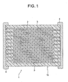
- a multilayer ceramic capacitor 1 as an electronic device has a capacitor element body 10 having a configuration that dielectric layers 2 and internal electrode layers 3 are alternately stacked. On both end portions of the capacitor element body 10, a pair of external electrodes 4 respectively connected to the internal electrode layers 3 alternately arranged inside the element body 10 are formed.
- a shape of the capacitor element body 10 is not particularly limited, but normally is rectangular parallelepiped. Also, a size thereof is not particularly limited and may be suitable size in accordance with the use object, but normally is (0.4 to 5.6 mm) ⁇ (0.2 to 5.0 mm) ⁇ (0.2 to 1.9 mm) or so.
- the internal electrode layers 3 are stacked so as to be alternately exposed to surfaces of two facing end portions of the capacitor element body 10.
- the pair of external electrodes 4 are formed at both end portions of the capacitor element body 10 and connected to exposed end surfaces of the alternately arranged internal electrode layers 3 so as to compose a capacitor circuit.
- the dielectric layer 2 includes the dielectric ceramic composition of the present invention.
- a dielectric ceramic composition of the present invention includes at least a main component containing a dielectric oxide having a composition expressed by [(Ca x Sr 1-x )O] m [(Ti y Zr 1-y-z Hf z )O 2 ], a first subcomponent containing a Mn oxide and/or an Al oxide, and a glass component.
- composition mole ratios in the main component are in relationships below. 0.90 ⁇ m ⁇ 1.04, preferably 1.005 ⁇ m ⁇ 1.025 0.5 ⁇ x ⁇ 1, preferably 0.6 ⁇ x ⁇ 0.9 0.01 ⁇ y ⁇ 0.10, preferably 0.02 ⁇ y ⁇ 0.07 0 ⁇ z ⁇ 0.20, preferably 0 ⁇ z ⁇ 0.10
- 0.2 to 5 mol% and more preferably 0.2 to 3 mol% of the Mn oxide in terms of MnO, and 0.1 to 10 mol%, and more preferably 0.1 to 5 mol% of an Al oxide in terms of Al 2 O 3 are included.
- the Mn oxide is added as a reduction resistance imparting agent and a sintering auxiliary.
- the adding quantity is too small, the sinterability declines, while when too large, it is liable that frequency dependency by the permittivity and a temperature coefficient of the capacitance increases and frequency dependency by the tan ⁇ increases.
- 0 to 2.5 mol% (note that 0 is excluded) and more preferably 0.5 to 2.5 mol% of a V oxide in terms of V 2 O 5 is included with respect to 100 mol% of the main component.
- the IR accelerated lifetime can be improved.
- the adding quantity is too small, it is liable that the effect of improving the IR accelerated lifetime is hard to be obtained, while when too much, sinterability tends to decline.
- the glass component contains at least SiO 2 as a main component.
- the glass component further contains BaO and CaO, and a composite oxide expressed by a general formula (Ba, Ca) x SiO 2+x is more preferable.
- the glass component is [(Ba v Ca 1-v )O] w SiO 2 (barium silicate / calcium), "v” and “w” in the composition formula of the glass component are in ranges of 0 ⁇ v ⁇ 1 and 0.5 ⁇ w ⁇ 4.0, and the glass component is included by 0.5 to 15 mol%, more preferably 0.1 to 5 mol% with respect to 100 mol% of the main component. Further preferably, the "v” and “w” in the formula of the glass component are in ranges of 0.5 ⁇ v ⁇ 1 and 0.55 ⁇ w ⁇ 3.0.
- the glass component is added as a sintering auxiliary.
- the adding quantity of the glass component is too small, the sinterability tends to decline, while when too much, it is liable that the sinterability is hindered.
- At least one of rare earth elements including Sc and Y is included by 0.02 to 1.5 mol% and more preferably 0.10 to 1.0 mol% with respect to 100 mol% of the main component.
- the rare earth elements include 17 elements composed of a lanthanoid.
- At least one of Nb, Mo, Ta, W and Mg is included by 0.02 to 1.5 mol% and more preferably 0.10 to 1.0 mol% with respect to 100 mol% of the main component.
- These elements may be combined with the above rare earth elements to be included in the dielectric ceramic composition.
- a total content thereof is preferably 0.02 to 1.5 mol% and more preferably 0.10 to 1.0 mol% with respect to 100 mol% of the main component.
- the dielectric layer 2 is composed of crystal grains and a grain boundary phase, and an average particle diameter of the crystal grain of the dielectric layer 2 is 2 ⁇ m or less.
- the grain boundary phase normally contains oxides of materials composing the dielectric material or internal electrode material, oxides of separately added materials and, furthermore, oxides of materials to be mixed in as impurities in the procedure, and is normally composed of glass or a vitreous material.
- a conductive material included in the internal electrode layer 3 is not particularly limited, and base metals may be used because composing material of the dielectric layer 2 has reducing resistance.
- the base metal to be used as the conductive material Ni or a Ni alloy is preferable.
- a Ni alloy an alloy of one or more kinds of elements selected from Mn, Cr, Co and Al with Ni is preferable, and a content of Ni in the alloy is preferably 95 wt% or more.
- the Ni or Ni alloy may contain various trace components, such as P, Fe and Mg, by not more than 0.1 wt% or so.
- a thickness of the internal electrode layer may be suitably determined in accordance with the use object, etc., but normally it is preferably 0.5 to 5 ⁇ m, and particularly 1 to 2.5 ⁇ m or so.
- a conductive material included in the external electrode 4 is not particularly limited, and Cu, a Cu alloy, Ni and Ni alloy, etc. are used. Of course, Ag and an Ag-Pd alloy, etc. may be also used. Note that inexpensive Ni, Cu and alloys of these are used in the present embodiment.
- a thickness of the external electrode may be suitably determined in accordance with the use object, etc., but normally 10 to 50 ⁇ m or so is preferable.
- a multilayer ceramic capacitor using the dielectric ceramic composition of the present invention is produced by forming a green chip by a normal printing method and sheet method using pastes, firing the same, then, printing or transferring external electrodes and firing in the same way as in a multilayer ceramic capacitor of the related art. Below, the production method will be explained specifically.
- the dielectric layer paste may be an organic paste obtained by kneading the dielectric material with an organic vehicle or a water based paste.
- the dielectric material in accordance with a composition of the dielectric ceramic composition according to the present invention explained above, materials composing the main component and subcomponents (including a glass component) are used.
- materials composing the main component and subcomponents including a glass component
- a form of the materials is not particularly limited and oxides composing the main component and subcomponents and/or compounds, which become oxides by firing, are used and the materials may be powder obtained by a liquid-phase synthesis method.
- oxides by firing for example, carbonate, oxalate, nitrate, hydroxide and organic metal compound, etc. may be mentioned.
- oxides and the compounds to be oxides by firing may be used together.
- a content of each compound in the dielectric material may be determined so as to attain the above explained composition of the dielectric ceramic composition after firing.
- the material powder those having an average particle diameter of 0.0005 to 1.5 ⁇ m or so are used in the present embodiment.
- An organic vehicle is obtained by dissolving a binder in an organic solvent.
- the binder to be used for the organic vehicle is not particularly limited and may be suitably selected from a variety of normal binders, such as ethyl cellulose and polyvinyl butyral.
- the organic solvent to be used here is not particularly limited and may be suitably selected from a variety of organic solvents, such as terpineol, butyl carbitol, acetone, and toluene, in accordance with a method to be used, such as the printing method and sheet method.
- a water based paste is obtained by dissolving a water-soluble binder and dispersant, etc. in water.
- the water-soluble binder is not particularly limited and may be suitably selected from polyvinyl alcohol, cellulose, water-soluble acrylic resin, and emulsion etc.
- the paste is not collectively fabricated by mixing the main component (base material) and subcomponents (additives) in a vehicle by the liquid-phase method, but the solid-phase method is used. Namely, after performing high dispersion mixing on the main component materials and subcomponent materials, the result is dried, then, calcinated at a time, and the result is mixed with a vehicle to fabricate the paste.
- the high dispersion mixing of the main component materials and subcomponent materials is performed, for example, by adding water as a medium respectively to the main component materials and subcomponent materials and mixing by a ball mill for 16 to 40 hours.
- a condition of the calcination is not particularly limited and, for example, 1100 to 1300°C for 2 to 4 hours.
- the calcinated result is subjected to wet grinding by a ball mill, etc., dried, then, fabricated to be a paste.
- the internal electrode layer paste is fabricated by kneading a conductive material formed by the above variety of conductive metals and alloys or a variety of oxides, organic metal compounds, and resinates, etc., which become the above conductive material after firing, with the above organic vehicle.
- the external electrode paste may be fabricated in the same way as in the case of the internal electrode layer paste explained above.
- a content of each of the above pastes and organic vehicle is not particularly limited and may be a normal content that, for example, the binder is 1 to 5 wt% or so and the solvent is 10 to 50 wt% or so.
- each paste may contain additives selected from a variety of dispersants, plasticizers, dielectrics, and insulator, etc. in accordance with need.
- the dielectric paste and the internal electrode paste are stacked by printing on a substrate of polyethylene terephhtalate, etc., cut to be a predetermined shape, then, released from the substrate to obtain a green chip.
- the dielectric paste is used for forming a green sheet, the internal electrode paste is printed thereon and, then, the results are stacked to obtain a green chip.
- the green chip is subjected to binder removal processing and firing.
- the binder removal processing may be performed under a normal condition, but particularly when using a base metal, such as Ni and a Ni alloy, as a conductive material of the internal electrode layer, it is performed in the air, the temperature rising rate is 5 to 300°C/hour and preferably 10 to 100°C, the holding temperature is 180 to 400°C and preferably 200 to 300°C, and the temperature holding time is 0.5 to 24 hours and preferably 5 to 20 hours.
- a base metal such as Ni and a Ni alloy
- a firing atmosphere of the green chip may be suitably determined in accordance with a kind of the conductive material in the internal electrode layer paste, but when using a base metal, such as Ni and a Ni alloy, as a conductive material, a reducing atmosphere is preferable, and the oxygen partial pressure of the firing atmosphere is preferably 10 -10 to 10 -3 Pa and more preferably 10 -7 to 10 -3 Pa (10 -5 to 10 -12 atm).
- the oxygen partial pressure at firing is too low, it is liable that the conductive material of the internal electrode is abnormally sintered, while when too high, the internal electrode tends to be oxidized.
- the holding temperature at the main firing is 1300°C or lower, preferably 1000 to 1300°C, and more preferably 1200 to 1300°C.
- the holding temperature is too low, densification tends to become insufficient, while when too high, the capacity-temperature characteristics tend to deteriorate as a result of breakings of electrodes due to abnormal sintering of the internal electrode or dispersion of the internal electrode layer material.
- the temperature rising rate is preferably 50 to 500°C/hour and more preferably 200 to 300°C/hour
- the temperature holding time is preferably 0.5 to 8 hours and more preferably 1 to 3 hours
- the cooling rate is preferably 50 to 500°C/hour and more preferably 200 to 300°C/hour.
- the firing atmosphere is preferably a reducing atmosphere and a preferable atmosphere gas is, for example, a wet mixed gas of nitrogen gas and hydrogen gas.
- annealing thermal treatment
- Annealing is processing for re-oxidizing the dielectric layer and the insulation resistance can be improved thereby.
- An oxygen partial pressure in the annealing atmosphere is preferably 10 -4 Pa or higher, and more preferably 1 to 10 -3 Pa (10 -5 to 10 -8 atm) .
- the oxygen partial pressure is too low, re-oxidization of the dielectric layer 2 tends to become difficult, while when too high, the internal electrode layer 3 tends to be oxidized.
- the holding temperature at annealing is preferably 1150°C or lower, and more preferably 500 to 1100°C.
- the holding temperature is too low, re-oxidization of the dielectric layer becomes insufficient, so that it is liable that the insulation resistance becomes low and the accelerated lifetime becomes short.
- the holding temperature is too high, not only the internal electrode layer is oxidized to reduce the capacity, but the internal electrode layer reacts with the dielectric base material, and it is liable that deterioration of the capacity-temperature characteristics, a decline of the insulation resistance and a decline of the accelerated lifetime are caused.
- the annealing may be composed only of a temperature rising step and a temperature lowering step. In this case, the temperature holding time is zero and the holding temperature becomes a synonym of the highest temperature.
- the temperature holding time is preferably 0 to 20 hours and more preferably 6 to 10 hours, and the cooling rate is preferably 50 to 500°C/hour and more preferably 100 to 300°C/hour.
- a preferable atmosphere gas to be used in the annealing is, for example, a wet nitrogen gas.
- a wetter, etc. may be used to wet the nitrogen gas and mixed gas, etc. in the above binder removal processing and annealing.
- the water temperature is preferably 5 to 75°C.
- the binder removal processing, firing and annealing may be performed continuously or separately.
- the atmosphere is changed without cooling after the binder removal processing, continuously, the temperature is raised to the holding temperature at firing to perform firing. Next, it is cooled and the thermal treatment is preferably performed by changing the atmosphere when the temperature reaches to the holding temperature of the thermal treatment.
- the atmosphere is changed, and the temperature is furthermore raised. After that, after cooling the temperature to the holding temperature at the annealing, it is preferable that the cooling continues by changing the atmosphere again to a nitrogen gas or a wet nitrogen gas.
- the atmosphere may be changed, or the entire process of the annealing may be in a wet nitrogen gas atmosphere.
- the thus obtained capacitor sintered body is subjected to end surface polishing, for example, by barrel polishing and sand-blast, etc., then, a terminal electrode paste is printed or transferred, and firing is performed to external electrodes 4.
- a firing condition of the external electrode paste is preferably at 600 to 800°C for 10 minutes to 1 hour or so in a wet mixed gas of nitrogen gas and hydrogen gas.
- soldering, etc. is performed on the external electrode 4 to form a cover layer (pad layer).
- the ceramic capacitor 1 of the present embodiment produced as above is mounted on a print substrate, etc. by soldering, etc. and used for a variety of electronic equipments.
- a multilayer ceramic capacitor was explained as an example of an electronic device according to the present invention, but an electronic device according to the present invention is not limited to the multilayer ceramic capacitor and may be any as far as it is composed of a dielectric ceramic composition having the above composition.
- main component materials SrCO 3 , CaCO 3 , TiO 2 , ZrO 2 and HfO 2
- subcomponent materials including a glass component each having an average particle diameter of 0.1 to 1.5 ⁇ m
- carbonate MnO 3 and BaCO 3
- oxides Al 2 O 3 , SiO 2 and Y 2 O 3 , etc.
- a green sheet having a thickness of 7 ⁇ m was formed on a PET film, after printing the internal electrode layer paste thereon, the green sheet was removed from the PET film.
- the green sheets and protective green sheets (not printed with the internal electrode layer paste) were stacked and bonded with pressure, so that a green chip was obtained.
- the number of the stacked sheets having an internal electrode was four.
- the green chip was cut to a predetermined size and subjected to binder removal processing, firing and annealing (thermal treatment), so that a multilayer ceramic fired body was obtained.
- the binder removal processing was performed under a condition of the temperature raising rate of 15°C/hour, the holding temperature of 280°C, the temperature holding time of 8 hours, and the atmosphere of in the air.
- the firing was performed under a condition of the temperature raising rate of 200°C/hour, the holding temperature of 1280°C, the temperature holding time of 2 hours, cooling rate of 300°C/hour and the atmosphere of wet mixed gas of N 2 and H 2 (the oxygen partial pressure was adjusted to be in a range of 2 ⁇ 10 -7 to 5 ⁇ 10 -3 Pa).
- the annealing was performed under a condition of the holding temperature of 900°C, the temperature holding time of 9 hours, cooling rate of 300°C/hour and the atmosphere of wet N 2 gas (the oxygen partial pressure was 3.54 ⁇ 10 -2 Pa). Note that a wetter, wherein the water temperature was 35°C, was used to wet the atmosphere gas at the time of firing and annealing.
- the external electrode paste was transferred to the end surfaces and fired at 800°C for 10 minutes in a wet N 2 + H 2 atmosphere to form external electrodes, so that samples of the multilayer ceramic capacitor having the configuration as shown in FIG. 1 were obtained.
- a size of the thus obtained samples was 3.2 mm ⁇ 1.6 mm ⁇ 0.6 mm, the number of dielectric layers sandwiched by internal electrode layers was 4, a thickness of one dielectric layer was 7 ⁇ m, and a thickness of one internal electrode layer was 2 ⁇ m. Evaluation of the characteristics below was made on the respective samples.
- a capacitance of the capacitor samples was measured under a condition of the reference temperature of 25°C, a frequency of 1 kHz, and an input signal level (measurement voltage) of 1 Vrms by using a digital LCR meter (4274A made by YHP). Then, the obtained capacitance, and an electrode size and a distance between electrodes in each capacitor sample were used for calculating the specific permittivity (no unit). After that, by using an insulation resistance tester (R8340A made by Advantest Corporation), insulation resistance IR after applying a direct current of 50V to the capacitor samples for 60 seconds at 25°C was measured. The results are shown in Table 2.
- the capacitance change rate ⁇ C125/C25 (ppm/°C) was calculated by the formula 1 below.
- ⁇ C125/C25 ⁇ (C125-C25)/C25 ⁇ (1/(125-25)) Note that "C125” indicates a capacitance at 125°C and “C25” indicates a capacitance at 25°C in the formula.
- the capacitor samples were kept in a state of being applied with a direct current voltage of 70 V/ ⁇ m at 200°C for measuring time until the resistance (IR) became 2 ⁇ 10 5 ⁇ by considering it as a high temperature load lifetime.
- the measurement of the high temperature load lifetime was made on 10 capacitor samples and the evaluation was made by obtaining the average lifetime. The results are shown in Table 2.
- Insulation resistance was measured on 1000 capacitor samples having the same composition by the same method of measuring insulation resistance explained above. Those exhibited 10 10 ⁇ or lower were considered defective and percentage of the defective samples was obtained.
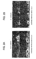
- FIG. 2B showing an enlarged picture of a section of a capacitor sample as an example corresponding to the sample number 3
- FIG. 2A showing an enlarged picture of a section of a capacitor sample as a comparative example corresponding to the sample number 10 shown in Table 1 and Table 2
- the average crystal particle diameter became small by adding Hf in the main component.
- capacitor samples were produced in the same way as in the example 1 and an evaluation was made in the same way as in the example 1. The results are shown in Table 11. Note that, in the present embodiment, dielectric loss (tan ⁇ ) of the capacitor samples was also measured by an LCR meter under a condition of 140°C and 20 Hz. Also, the results of measuring temperature dependency by tan ⁇ in the capacitor samples are shown in FIG. 4B.
- Capacitor samples were produced in the same way as in the sample numbers 70 to 72 in the example 6 other than collectively fabricating a dielectric paste not by the solid-phase method but by the liquid-phase method, and in the same way as in the example 6 other than performing main firing at a temperature of 1220 to 1300°C. An evaluation was made in the same way as in the example 6. The results are shown in Table 12. Also, results of measuring temperature dependency by tan ⁇ of the capacitor samples are shown in FIG. 4A.
- capacitor samples were produced in the same way as in the case of the sample number 10 in the example 1 and an evaluation was made in the same way as in the example 1.
- Table 13 Note that, in the present embodiment, X-ray analysis was also performed on dielectric layers of the capacitor samples, and a CV value (variation coefficient) indicating dispersibility of respective elements in the dielectric layers was also measured as shown in Table 13.
- the CV value is defined as a value obtained by calculating standard deviation D(x) from an X-ray intensity distribution of each element in the dielectric layer and dividing the standard deviation D(x) by an expectation value E(x) of the X-ray intensity distribution of each element.
- the dispersibility is preferable.
- the CV value (variation coefficient) indicating dispersibility of each element in the dielectric layer was measured on capacitor samples having a composition of the sample number 3 (Hf is added) in the example 1 in the same way as in the reference example 2. The results are shown in Table 13.
- a highly reliable nonreducing dielectric ceramic composition preferably used as a dielectric layer of a multilayer ceramic capacitor, etc. using a base metal, such as Ni, as an internal electrode and able to be sintered at 1300°C or lower; wherein a temperature coefficient of the capacitance is small and able to be freely controlled in a range of -15 to +150 ppm/°C, the insulation resistance at 25°C is 1 ⁇ 10 13 ⁇ or higher, the specific permittivity and dielectric loss tangent (tan ⁇ ) have a little frequency dependency, accelerated lifetime of the insulation resistance is long, and a insulation resistance defect rate is low even when the insulation layer is made thin.
- a base metal such as Ni
Landscapes
- Chemical & Material Sciences (AREA)
- Engineering & Computer Science (AREA)
- Ceramic Engineering (AREA)
- Manufacturing & Machinery (AREA)
- Inorganic Chemistry (AREA)
- Structural Engineering (AREA)
- Materials Engineering (AREA)
- Organic Chemistry (AREA)
- Power Engineering (AREA)
- Microelectronics & Electronic Packaging (AREA)
- Composite Materials (AREA)
- Inorganic Insulating Materials (AREA)
- Ceramic Capacitors (AREA)
- Compositions Of Oxide Ceramics (AREA)
- Fixed Capacitors And Capacitor Manufacturing Machines (AREA)
Abstract
A dielectric ceramic composition, comprising a main
component including at least a dielectric oxide having a
composition expressed by [(CaxSr1-x)O]m[(TiyZr1-y-zHfz)O2], a
first subcomponent including a Mn oxide and/or an Al
oxide and a glass component, wherein "m", "x", "y" and
"z" indicating composition mole ratios in the formula
included in the main component are in relationships of
0.90 ≤ m ≤ 1.04, preferably 1.005 ≤ m ≤ 1.025, 0.5 ≤ x <
1, preferably 0.6 ≤ x ≤ 0.9, 0.01 ≤ y ≤ 0.10, preferably
0.02 ≤ y ≤ 0.07 and 0 < z ≤ 0.20, preferably 0 < z ≤ 0.10.
Description
The present invention relates to a dielectric
ceramic composition, an electronic device and production
methods of them, and particularly relates to a
nonreducing temperature compensating dielectric ceramic
composition preferably used for an electronic device,
such as a multilayer ceramic capacitor, using a base
metal as an internal electrode thereof.
Multilayer ceramic capacitors are widely used as
electronic devices, and the number used in one electronic
device is also large. A multilayer ceramic capacitor is
normally produced by stacking an internal electrode layer
paste and a dielectric layer paste by a sheet method or a
printing method, etc. and cofiring the result.
A dielectric ceramic material used for a multilayer
ceramic capacitor, etc. of the related art has a property
of getting reduced and becoming a semiconductor when
fired in a reducing atmosphere. Therefore, as an internal
electrode material, Pd and other precious metals, which
do not melt at a temperature of sintering the dielectric
ceramic material and are not oxidized even if fired under
a high oxygen partial pressure of not bringing the
dielectric ceramic material to be a semiconductor, have
been used.
However, high prices of Pd and other precious
metals have hindered a cost reduction of the multilayer
ceramic capacitor much. Thus, use of relatively
inexpensive base metals, such as Ni and a Ni alloy, as
the internal electrode material has become dominant.
When using a base metal as a conductive material of
the internal electrode layer, however, the internal
electrode layer is oxidized when fired in the air.
Accordingly, cofiring of the dielectric layer and
internal electrode layer has to be performed in a
reducing atmosphere.
However, when fired in a reducing atmosphere, the
dielectric layer is reduced and the insulation resistance
becomes low. Therefore, a nonreducing dielectric material
has been proposed. But again, a multilayer ceramic
capacitor using a nonreducing dielectric material has a
disadvantage that the insulation resistance (IR) becomes
poor when a thickness of the dielectric layer is made
thin (5 µm or thinner) according to a reliability test.
On the other hand, demands have become stronger for
a temperature compensating dielectric ceramic composition,
wherein a temperature change of the capacitance is small,
that is the capacitor-temperature coefficient is small,
and able to be freely controlled in a range of -50 to
+150 ppm/°C, so that a ceramic material capable of
providing such a capacitor having a controllable low
temperature coefficient has become necessary.
Note that, as described in the Japanese Patent
Publication No. 2997236, there has been a proposal of a
highly reliable nonreducing dielectric ceramic
composition able to be sintered at 1300°C or lower,
wherein a temperature coefficient of the capacitance is
small and able to be freely controlled in a range of -15
to +150 ppm/°C, the insulation resistance at 25°C is
1×10¹³ Ω or higher, the specific permittivity and
dielectric loss tangent (tanδ) have a little frequency
dependency, and accelerated lifetime of the insulation
resistance is long even when the insulation layer is made
thin. The dielectric ceramic composition is preferably
used for a multilayer ceramic capacitor using a base
metal, such as Ni, as an internal electrode.
However, experiments by the present inventors
proved that the dielectric ceramic composition described
in the above patent article 1 has uneven insulation
resistance and is hard to reduce the insulation
resistance defect rate.
The present invention was made in consideration of
the above circumstances and has as an object thereof to
provide highly reliable nonreducing dielectric ceramic
composition preferably used as a dielectric layer of a
multilayer ceramic capacitor, etc. using Ni or other base
metal as the internal electrode, and able to be sintered
at 1300°C or lower, wherein a temperature coefficient of
the capacitance is small and able to be freely controlled
in a range of -15 to +150 ppm/°C, the insulation
resistance at 25°C is 1×10¹³ Ω or higher, the specific
permittivity and dielectric loss tangent (tanδ) have a
little frequency dependency, accelerated lifetime of the
insulation resistance is long and, moreover, a defect
rate of the insulation resistance is low even when the
insulation layer is made thin.
Also, another object of the present invention is to
provide an electronic device, such as a multilayer
ceramic capacitor, having a dielectric ceramic
composition having the above characteristics as the
dielectric layer, and production methods for producing
the dielectric ceramic composition and the electronic
device unfailingly with high productivity.
To attain the above objects, according to the
present invention, there is provided a dielectric ceramic
composition including at least
a main component containing a dielectric oxide having a composition expressed by [(CaxSr1-x)0]m[(TiyZr1-y-z zHfz)O2],
a first subcomponent containing a Mn oxide and/or an Al oxide, and
a glass component:
a main component containing a dielectric oxide having a composition expressed by [(CaxSr1-x)0]m[(TiyZr1-y-z zHfz)O2],
a first subcomponent containing a Mn oxide and/or an Al oxide, and
a glass component:
0.90 ≤ m ≤ 1.04, preferably 1.005 ≤ m ≤ 1.025,
0.5 ≤ x < 1, preferably 0.6 ≤ x ≤ 0.9,
0.01 ≤ y ≤ 0.10, preferably 0.02 ≤ y ≤ 0.07,
0 < z ≤ 0.20 preferably 0 < z ≤ 0.10.
The dielectric ceramic composition according to the
present invention basically has approximately the same
composition as that in the patent article 1, so that it
is possible to provide a highly reliable nonreducing
dielectric ceramic composition able to be sintered at
1300°C or lower, wherein a temperature coefficient of the
capacitance is small and able to be freely controlled in
a range of -15 to +150 ppm/°C, the insulation resistance
at 25°C is 1×10¹³ Ω or higher, the specific permittivity
and dielectric loss tangent (tanδ) have a little
frequency dependency, and accelerated lifetime of the
insulation resistance is long even when the insulation
layer is made thin.
Particularly, in the present invention, being
different from the patent article 1, Hf is added to the
main component, so that a shrinkage curve at sintering
becomes gentle comparing with that of a composition not
added with Hf, and cracks and delamination are hard to be
generated at the time of cofiring with an internal
electrode. Also, since Hf is added to the main component,
crystal grain growth is suppressed and a fine and uniform
crystal can be realized comparing with the case of a
composition not added with Hf. These were proved by the
experiments by the present inventors.
As a result, according to the present invention,
unevenness of insulation resistance caused by unevenness
of the boundary face due to cracks, delamination or an
uneven crystal can be suppressed.
Note that, in the present invention, when an x-value
in the composition formula of the main component is
too small, frequency dependency by the capacitance and
tanδ tends to increase, while when too large, the
sinterability tends to decline.
Also, when a y-value in the composition formula is
too small, the sinterability tends to decline, while when
too large, frequency dependency by the capacitance and
tanδ tends to increase.
Furthermore, when a z-value in the composition
formula is too small, frequency dependency by the
capacitance and tanδ tends to increase, while when too
large, the sinterability tends to decline.
Furthermore, when an m-value in the composition
formula is too small, frequency dependency by the
capacitance and tanδ tends to increase, while when too
large, it is liable that firing at a temperature of
1300°C or lower becomes difficult.
Preferably, with respect to 100 mol% of the main
component, 0.2 to 5 mol%, and more preferably 0.2 to 3
mol% of the Mn oxide in terms of MnO, and 0.1 to 10 mol%,
and more preferably 0.1 to 5 mol% of an Al oxide in terms
of Al2O3 are included.
The Mn oxide is added as a reduction resistance
imparting agent and a sintering auxiliary. When the
adding quantity is too small, the sinterability declines,
while when too large, it is liable that frequency
dependency by the permittivity and a temperature
coefficient of the capacitance increases and frequency
dependency by the tanδ increases.
Also, when an adding quantity of the Al oxide is
too small, the insulation resistance and sinterability
decline, while when too much, the relative permittivity
tends to decline.
Preferably, 0 to 2.5 mol% (note that 0 is excluded)
and more preferably 0.5 to 2.5 mol% of a V oxide in terms
of V2O5 is included with respect to 100 mol% of the main
component.
By adding the V oxide, the IR accelerated lifetime
can be improved. When the adding quantity is too small,
it is liable that the effect of improving the IR
accelerated lifetime is hard to be obtained, while when
too much, sinterability tends to decline.
Preferably, the glass component contains at least
SiO2 as a main component.
Also, the glass component further contains BaO and CaO, and a composite oxide expressed by a general formula (Ba, Ca)xSiO2+x is more preferable.
Also, the glass component further contains BaO and CaO, and a composite oxide expressed by a general formula (Ba, Ca)xSiO2+x is more preferable.
Preferably, the glass component is [(BavCa1-v)O]wSiO2
(barium silicate / calcium), "v" and "w" in the
composition formula of the glass component are in ranges
of 0 ≤ v ≤ 1 and 0.5 ≤ w ≤ 4.0, and the glass component
is included by 0.5 to 15 mol%, more preferably 0.1 to 5
mol% with respect to 100 mol% of the main component.
Further preferably, the "v" and "w" in the formula of the
glass component are in ranges of 0.5 ≤ v ≤ 1 and 0.55 ≤ w
≤ 3.0.
When the v-value in the composition formula of the
vitreous component is too small, it is liable that the IR
accelerated lifetime tends to become short, while when
the v-value is too large, sinterability tends to decline
when the dielectric layer is made as thin as 5 µm or
thinner.
The glass component is added as a sintering
auxiliary. When the adding quantity of the glass
component is too small, the sinterability tends to
decline, while when too much, it is liable that the
sinterability is hindered.
Preferably, at least one of rare earth elements
including Sc and Y is included by 0.02 to 1.5 mol% and
more preferably 0.10 to 1.0 mol% with respect to 100 mol%
of the main component. Note that, besides Sc and Y, the
rare earth elements include 17 elements composed of a
lanthanoid.
Preferably, at least one of Nb, Mo, Ta, W and Mg is
included by 0.02 to 1.5 mol% and more preferably 0.10 to
1.0 mol% with respect to 100 mol% of the main component.
These elements may be combined with the above rare earth
elements to be included in the dielectric ceramic
composition. In that case, a total content thereof is
preferably 0.02 to 1.5 mol% and more preferably 0.10 to
1.0 mol% with respect to 100 mol% of the main component.
By adding oxides of these elements (including the
rare earth elements), frequency dependency by a
temperature coefficient of the capacitance and tanδ can
be suppressed. When an adding quantity of these oxides
are too small, it is liable that the effect of
suppressing frequency dependency by a temperature
coefficient of the capacitance and tanδ is hard to be
obtained, while when too large, the sintering temperature
tends to become high.
According to the present invention, there is
provided a production method of any one of the dielectric
ceramic compositions explained above, comprising the
steps of:
Preferably, in the step of mixing the materials,
high dispersion mixture is performed until an average
particle diameter of the mixture composed of the main
component, glass component and subcomponent becomes 1.0
µm or less.
In the method of the present invention, solid
solubility of the glass component and subcomponents to
the main component is uniformly accelerated, so that
reactivity becomes gentle in main firing and abrupt grain
growth can be suppressed. As a result, crystal particle
diameters become uniform and fine and able to be
sufficiently sintered at a temperature of 1300°C or lower,
so that it becomes possible to realize a thinner layer.
Also, in the method of the present invention, a stress
from the internal electrode is lightened when thermally
contracted at the time of the main firing, so that crack
defectives are reduced.
Preferably, the calcinated substance is mixed with
a binder to prepare a dielectric paste, the dielectric
paste is subjected to main firing, and a temperature of
the main firing is 1300°C or lower.
An average particle diameter of a crystal in the
dielectric ceramic composition obtained after performing
main firing on the calcinated substance is preferably 2
µm or smaller, more preferably 1.5 µm or smaller, and
particularly preferably 1.0 µm or smaller.
When the average particle diameter of the crystal
is too large, it is liable that the IR accelerated
lifetime becomes short and reliability declines, for
example, when the dielectric layer in a multilayer
ceramic capacitor is made as thin as 5 µm or thinner.
The dielectric ceramic composition according to the
present invention is preferably produced by the method
described above.
According to the present invention, there is
provided an electronic device having a dielectric layer,
wherein the dielectric layer is composed of any one of
the dielectric ceramic compositions explained above.
Preferably, an electronic device according to the
present invention is an electronic device, such as a
multilayer ceramic capacitor, having alternately stacked
internal electrodes and dielectric layers.
Preferably, the internal electrode includes at
least nickel or other base metal.
Preferably, an average particle diameter of a
crystal in the dielectric layer is 2 µm or less.
In the production method of an electronic device
according to the present invention, main firing at 1300°C
or lower is performed on the internal electrodes and
dielectric layers at a time.
These and other objects and features of the present
invention will become clearer from the following
description of the preferred embodiments given with
reference to the attached drawings, in which:
Below, the present invention will be explained in
detail based on embodiments shown in the drawings.
As shown in FIG. 1, a multilayer ceramic capacitor
1 as an electronic device according to an embodiment of
the present invention has a capacitor element body 10
having a configuration that dielectric layers 2 and
internal electrode layers 3 are alternately stacked. On
both end portions of the capacitor element body 10, a
pair of external electrodes 4 respectively connected to
the internal electrode layers 3 alternately arranged
inside the element body 10 are formed. A shape of the
capacitor element body 10 is not particularly limited,
but normally is rectangular parallelepiped. Also, a size
thereof is not particularly limited and may be suitable
size in accordance with the use object, but normally is
(0.4 to 5.6 mm) × (0.2 to 5.0 mm) × (0.2 to 1.9 mm) or so.
The internal electrode layers 3 are stacked so as
to be alternately exposed to surfaces of two facing end
portions of the capacitor element body 10. The pair of
external electrodes 4 are formed at both end portions of
the capacitor element body 10 and connected to exposed
end surfaces of the alternately arranged internal
electrode layers 3 so as to compose a capacitor circuit.
The dielectric layer 2 includes the dielectric
ceramic composition of the present invention.
A dielectric ceramic composition of the present invention includes at least
a main component containing a dielectric oxide having a composition expressed by [(CaxSr1-x)O]m[(TiyZr1-y-zHfz)O2],
a first subcomponent containing a Mn oxide and/or an Al oxide, and
a glass component.
A dielectric ceramic composition of the present invention includes at least
a main component containing a dielectric oxide having a composition expressed by [(CaxSr1-x)O]m[(TiyZr1-y-zHfz)O2],
a first subcomponent containing a Mn oxide and/or an Al oxide, and
a glass component.
In the formula, "m", "x", "y" and "z" indicating
composition mole ratios in the main component are in
relationships below.
0.90 ≤ m ≤ 1.04, preferably 1.005 ≤ m ≤ 1.025
0.5 ≤ x < 1, preferably 0.6 ≤ x ≤ 0.9
0.01 ≤ y ≤ 0.10, preferably 0.02 ≤ y ≤ 0.07
0 < z ≤ 0.20, preferably 0 < z ≤ 0.10
0.90 ≤ m ≤ 1.04, preferably 1.005 ≤ m ≤ 1.025
0.5 ≤ x < 1, preferably 0.6 ≤ x ≤ 0.9
0.01 ≤ y ≤ 0.10, preferably 0.02 ≤ y ≤ 0.07
0 < z ≤ 0.20, preferably 0 < z ≤ 0.10
When the x-vale in the composition formula of the
main component is too small, it is liable that frequency
dependency by the capacitance and tanδ increases, while
when too large, the sinterability tends to decline.
Also, when a y-value in the composition formula is
too small, the sinterability tends to decline, while when
too large, frequency dependency by the capacitance and
tanδ tends to increase.
Furthermore, when a z-value in the composition
formula is too small, frequency dependency by the
capacitance and tanδ tends to increase, while when too
large, the sinterability tends to decline.
Furthermore, when an m-value in the composition
formula is too small, frequency dependency by the
capacitance and tanδ tends to increase, while when too
large, it is liable that firing at a temperature of
1300°C or lower becomes difficult.
Preferably, with respect to 100 mol% of the main
component, 0.2 to 5 mol%, and more preferably 0.2 to 3
mol% of the Mn oxide in terms of MnO, and 0.1 to 10 mol%,
and more preferably 0.1 to 5 mol% of an Al oxide in terms
of Al2O3 are included.
The Mn oxide is added as a reduction resistance
imparting agent and a sintering auxiliary. When the
adding quantity is too small, the sinterability declines,
while when too large, it is liable that frequency
dependency by the permittivity and a temperature
coefficient of the capacitance increases and frequency
dependency by the tanδ increases.
Also, when an adding quantity of the A1 oxide is
too small, the insulation resistance and sinterability
decline, while when too much, the relative permittivity
tends to decline.
Preferably, 0 to 2.5 mol% (note that 0 is excluded)
and more preferably 0.5 to 2.5 mol% of a V oxide in terms
of V2O5 is included with respect to 100 mol% of the main
component.
By adding the V oxide, the IR accelerated lifetime
can be improved. When the adding quantity is too small,
it is liable that the effect of improving the IR
accelerated lifetime is hard to be obtained, while when
too much, sinterability tends to decline.
Preferably, the glass component contains at least
SiO2 as a main component.
Also, the glass component further contains BaO and
CaO, and a composite oxide expressed by a general formula
(Ba, Ca)xSiO2+x is more preferable.
Preferably, the glass component is [(BavCa1-v)O]wSiO2
(barium silicate / calcium), "v" and "w" in the
composition formula of the glass component are in ranges
of 0 ≤ v ≤ 1 and 0.5 ≤ w ≤ 4.0, and the glass component
is included by 0.5 to 15 mol%, more preferably 0.1 to 5
mol% with respect to 100 mol% of the main component.
Further preferably, the "v" and "w" in the formula of the
glass component are in ranges of 0.5 ≤ v ≤ 1 and 0.55 ≤ w
≤ 3.0.
When the v-value in the composition formula of the
vitreous component is too small, it is liable that the IR
accelerated lifetime tends to become short, while when
the v-value is too large, sinterability tends to decline
when the dielectric layer is made as thin as 5 µm or
thinner.
The glass component is added as a sintering
auxiliary. When the adding quantity of the glass
component is too small, the sinterability tends to
decline, while when too much, it is liable that the
sinterability is hindered.
Preferably, at least one of rare earth elements
including Sc and Y is included by 0.02 to 1.5 mol% and
more preferably 0.10 to 1.0 mol% with respect to 100 mol%
of the main component. Note that, besides Sc and Y, the
rare earth elements include 17 elements composed of a
lanthanoid.
Preferably, at least one of Nb, Mo, Ta, W and Mg is
included by 0.02 to 1.5 mol% and more preferably 0.10 to
1.0 mol% with respect to 100 mol% of the main component.
These elements may be combined with the above rare earth
elements to be included in the dielectric ceramic
composition. In that case, a total content thereof is
preferably 0.02 to 1.5 mol% and more preferably 0.10 to
1.0 mol% with respect to 100 mol% of the main component.
By adding oxides of these elements (including the
rare earth elements), frequency dependency by a
temperature coefficient of the capacitance and tanδ can
be suppressed. When an adding quantity of these oxides
are too small, it is liable that the effect of
suppressing frequency dependency by a temperature
coefficient of the capacitance and tanδ is hard to be
obtained, while when too large, the sintering temperature
tends to become high.
Note that the number of stacked layers and
thickness of the dielectric layer 2 shown in FIG. 1 and
other conditions may be suitably determined in accordance
with the use object. It is preferable that the dielectric
layer 2 is composed of crystal grains and a grain
boundary phase, and an average particle diameter of the
crystal grain of the dielectric layer 2 is 2 µm or less.
The grain boundary phase normally contains oxides of
materials composing the dielectric material or internal
electrode material, oxides of separately added materials
and, furthermore, oxides of materials to be mixed in as
impurities in the procedure, and is normally composed of
glass or a vitreous material.
A conductive material included in the internal
electrode layer 3 is not particularly limited, and base
metals may be used because composing material of the
dielectric layer 2 has reducing resistance. As the base
metal to be used as the conductive material, Ni or a Ni
alloy is preferable. As a Ni alloy, an alloy of one or
more kinds of elements selected from Mn, Cr, Co and Al
with Ni is preferable, and a content of Ni in the alloy
is preferably 95 wt% or more. Note that the Ni or Ni
alloy may contain various trace components, such as P, Fe
and Mg, by not more than 0.1 wt% or so.
A thickness of the internal electrode layer may be
suitably determined in accordance with the use object,
etc., but normally it is preferably 0.5 to 5 µm, and
particularly 1 to 2.5 µm or so.
A conductive material included in the external
electrode 4 is not particularly limited, and Cu, a Cu
alloy, Ni and Ni alloy, etc. are used. Of course, Ag and
an Ag-Pd alloy, etc. may be also used. Note that
inexpensive Ni, Cu and alloys of these are used in the
present embodiment. A thickness of the external electrode
may be suitably determined in accordance with the use
object, etc., but normally 10 to 50 µm or so is
preferable.
A multilayer ceramic capacitor using the dielectric
ceramic composition of the present invention is produced
by forming a green chip by a normal printing method and
sheet method using pastes, firing the same, then,
printing or transferring external electrodes and firing
in the same way as in a multilayer ceramic capacitor of
the related art. Below, the production method will be
explained specifically.
First, a dielectric layer paste, internal electrode
paste and external electrode paste are produced,
respectively.
The dielectric layer paste may be an organic paste
obtained by kneading the dielectric material with an
organic vehicle or a water based paste.
As the dielectric material, in accordance with a
composition of the dielectric ceramic composition
according to the present invention explained above,
materials composing the main component and subcomponents
(including a glass component) are used. Note that a form
of the materials is not particularly limited and oxides
composing the main component and subcomponents and/or
compounds, which become oxides by firing, are used and
the materials may be powder obtained by a liquid-phase
synthesis method.
Note that, as compounds to become oxides by firing,
for example, carbonate, oxalate, nitrate, hydroxide and
organic metal compound, etc. may be mentioned. Of course,
oxides and the compounds to be oxides by firing may be
used together. A content of each compound in the
dielectric material may be determined so as to attain the
above explained composition of the dielectric ceramic
composition after firing. As the material powder, those
having an average particle diameter of 0.0005 to 1.5 µm
or so are used in the present embodiment.
An organic vehicle is obtained by dissolving a
binder in an organic solvent. The binder to be used for
the organic vehicle is not particularly limited and may
be suitably selected from a variety of normal binders,
such as ethyl cellulose and polyvinyl butyral. Also, the
organic solvent to be used here is not particularly
limited and may be suitably selected from a variety of
organic solvents, such as terpineol, butyl carbitol,
acetone, and toluene, in accordance with a method to be
used, such as the printing method and sheet method.
Also, a water based paste is obtained by dissolving
a water-soluble binder and dispersant, etc. in water. The
water-soluble binder is not particularly limited and may
be suitably selected from polyvinyl alcohol, cellulose,
water-soluble acrylic resin, and emulsion etc.
In the present embodiment, the paste is not
collectively fabricated by mixing the main component
(base material) and subcomponents (additives) in a
vehicle by the liquid-phase method, but the solid-phase
method is used. Namely, after performing high dispersion
mixing on the main component materials and subcomponent
materials, the result is dried, then, calcinated at a
time, and the result is mixed with a vehicle to fabricate
the paste.
The high dispersion mixing of the main component
materials and subcomponent materials is performed, for
example, by adding water as a medium respectively to the
main component materials and subcomponent materials and
mixing by a ball mill for 16 to 40 hours. A condition of
the calcination is not particularly limited and, for
example, 1100 to 1300°C for 2 to 4 hours. The calcinated
result is subjected to wet grinding by a ball mill, etc.,
dried, then, fabricated to be a paste.
The internal electrode layer paste is fabricated by
kneading a conductive material formed by the above
variety of conductive metals and alloys or a variety of
oxides, organic metal compounds, and resinates, etc.,
which become the above conductive material after firing,
with the above organic vehicle. The external electrode
paste may be fabricated in the same way as in the case of
the internal electrode layer paste explained above.
A content of each of the above pastes and organic
vehicle is not particularly limited and may be a normal
content that, for example, the binder is 1 to 5 wt% or so
and the solvent is 10 to 50 wt% or so. Also, each paste
may contain additives selected from a variety of
dispersants, plasticizers, dielectrics, and insulator,
etc. in accordance with need.
When using the printing method, the dielectric
paste and the internal electrode paste are stacked by
printing on a substrate of polyethylene terephhtalate,
etc., cut to be a predetermined shape, then, released
from the substrate to obtain a green chip. On the other
hand, when using the sheet method, the dielectric paste
is used for forming a green sheet, the internal electrode
paste is printed thereon and, then, the results are
stacked to obtain a green chip.
Next, the green chip is subjected to binder removal
processing and firing.
The binder removal processing may be performed
under a normal condition, but particularly when using a
base metal, such as Ni and a Ni alloy, as a conductive
material of the internal electrode layer, it is performed
in the air, the temperature rising rate is 5 to
300°C/hour and preferably 10 to 100°C, the holding
temperature is 180 to 400°C and preferably 200 to 300°C,
and the temperature holding time is 0.5 to 24 hours and
preferably 5 to 20 hours.
A firing atmosphere of the green chip may be
suitably determined in accordance with a kind of the
conductive material in the internal electrode layer paste,
but when using a base metal, such as Ni and a Ni alloy,
as a conductive material, a reducing atmosphere is
preferable, and the oxygen partial pressure of the firing
atmosphere is preferably 10-10 to 10-3 Pa and more
preferably 10-7 to 10-3 Pa (10-5 to 10-12 atm). When the
oxygen partial pressure at firing is too low, it is
liable that the conductive material of the internal
electrode is abnormally sintered, while when too high,
the internal electrode tends to be oxidized.
The holding temperature at the main firing is
1300°C or lower, preferably 1000 to 1300°C, and more
preferably 1200 to 1300°C. When the holding temperature
is too low, densification tends to become insufficient,
while when too high, the capacity-temperature
characteristics tend to deteriorate as a result of
breakings of electrodes due to abnormal sintering of the
internal electrode or dispersion of the internal
electrode layer material.
As other firing conditions, the temperature rising
rate is preferably 50 to 500°C/hour and more preferably
200 to 300°C/hour, the temperature holding time is
preferably 0.5 to 8 hours and more preferably 1 to 3
hours, and the cooling rate is preferably 50 to
500°C/hour and more preferably 200 to 300°C/hour. Also,
the firing atmosphere is preferably a reducing atmosphere
and a preferable atmosphere gas is, for example, a wet
mixed gas of nitrogen gas and hydrogen gas.
When firing in a reducing atmosphere, it is
preferable that annealing (thermal treatment) is
performed on a sintered body of the capacitor chip.
Annealing is processing for re-oxidizing the
dielectric layer and the insulation resistance can be
improved thereby. An oxygen partial pressure in the
annealing atmosphere is preferably 10-4 Pa or higher, and
more preferably 1 to 10-3 Pa (10-5 to 10-8 atm) . When the
oxygen partial pressure is too low, re-oxidization of the
dielectric layer 2 tends to become difficult, while when
too high, the internal electrode layer 3 tends to be
oxidized.
The holding temperature at annealing is preferably
1150°C or lower, and more preferably 500 to 1100°C. When
the holding temperature is too low, re-oxidization of the
dielectric layer becomes insufficient, so that it is
liable that the insulation resistance becomes low and the
accelerated lifetime becomes short. On the other hand,
when the holding temperature is too high, not only the
internal electrode layer is oxidized to reduce the
capacity, but the internal electrode layer reacts with
the dielectric base material, and it is liable that
deterioration of the capacity-temperature characteristics,
a decline of the insulation resistance and a decline of
the accelerated lifetime are caused. Note that the
annealing may be composed only of a temperature rising
step and a temperature lowering step. In this case, the
temperature holding time is zero and the holding
temperature becomes a synonym of the highest temperature.
As other annealing conditions, the temperature
holding time is preferably 0 to 20 hours and more
preferably 6 to 10 hours, and the cooling rate is
preferably 50 to 500°C/hour and more preferably 100 to
300°C/hour. Also, a preferable atmosphere gas to be used
in the annealing is, for example, a wet nitrogen gas.
In the same way as in the firing explained above,
for example, a wetter, etc. may be used to wet the
nitrogen gas and mixed gas, etc. in the above binder
removal processing and annealing. In this case, the water
temperature is preferably 5 to 75°C.
The binder removal processing, firing and annealing
may be performed continuously or separately. When
performing continuously, the atmosphere is changed
without cooling after the binder removal processing,
continuously, the temperature is raised to the holding
temperature at firing to perform firing. Next, it is
cooled and the thermal treatment is preferably performed
by changing the atmosphere when the temperature reaches
to the holding temperature of the thermal treatment. On
the other hand, when performing them separately, after
raising the temperature to the holding temperature at the
binder removal processing in an atmosphere of a nitrogen
gas or a wet nitrogen gas, the atmosphere is changed, and
the temperature is furthermore raised. After that, after
cooling the temperature to the holding temperature at the
annealing, it is preferable that the cooling continues by
changing the atmosphere again to a nitrogen gas or a wet
nitrogen gas. Also, in the annealing, after raising the
temperature to the holding temperature under the nitrogen
gas atmosphere, the atmosphere may be changed, or the
entire process of the annealing may be in a wet nitrogen
gas atmosphere.
The thus obtained capacitor sintered body is
subjected to end surface polishing, for example, by
barrel polishing and sand-blast, etc., then, a terminal
electrode paste is printed or transferred, and firing is
performed to external electrodes 4. A firing condition of
the external electrode paste is preferably at 600 to
800°C for 10 minutes to 1 hour or so in a wet mixed gas
of nitrogen gas and hydrogen gas. In accordance with need,
soldering, etc. is performed on the external electrode 4
to form a cover layer (pad layer).
The ceramic capacitor 1 of the present embodiment
produced as above is mounted on a print substrate, etc.
by soldering, etc. and used for a variety of electronic
equipments.
Note that the present invention is not limited to
the above embodiments and may be variously modified
within the scope of the present invention.
For example, in the above embodiment, a multilayer
ceramic capacitor was explained as an example of an
electronic device according to the present invention, but
an electronic device according to the present invention
is not limited to the multilayer ceramic capacitor and
may be any as far as it is composed of a dielectric
ceramic composition having the above composition.
Next, the present invention will be explained
further in detail by taking more specific examples of the
embodiment of the present invention, but the present
invention is not limited to the examples.
First, as starting materials for producing a
dielectric material, main component materials (SrCO3,
CaCO3, TiO2, ZrO2 and HfO2) and subcomponent materials
(including a glass component) each having an average
particle diameter of 0.1 to 1.5 µm were prepared. As the
subcomponent materials, carbonate (MnO3 and BaCO3) or
oxides (Al2O3, SiO2 and Y2O3, etc.) were used.
After weighing the materials, so that a composition
after firing would be the composition shown in Table 1
below, water as a medium was added to the materials and
mixed by a ball mill for 16 to 40 hours to perform high
dispersion mixing. After that, the mixture was dried,
then, calcinated under a condition of 1100 to 1300°C for
2 to 4 hours. Thus obtained calcinated substance was
subjected to wet grinding by a ball mill and dried.
With 100 parts by weight of the thus obtained dried
dielectric material, 4.8 parts by weight of an acrylic
resin, 40 parts by weight of methylene chloride, 20 parts
by weight of ethyl acetate, 6 parts by weight of mineral
spirit, and 4 parts by weight of acetone were mixed by a
ball mill to form a paste, so that a dielectric layer
paste was obtained.
Next, 100 parts by weight of Ni particles, 40 parts
by weight of an organic vehicle (obtained by dissolving 8
parts by weight of ethyl cellulose in 92 parts by weight
of butyl carbitol) and 10 parts by weight of butyl
carbitol were kneaded by three-roll to form a paste, so
that an internal electrode layer paste was obtained.
Next, 100 parts by weight of Cu particles, 35 parts
by weight of an organic vehicle (obtained by dissolving 8
parts by weight of an ethyl cellulose resin in 92 parts
by weight of butyl carbitol) and 7 parts by weight of
butyl carbitol were kneaded by three-roll to form a paste,
so that an external electrode paste was obtained.
Next, by using the dielectric layer paste, a green
sheet having a thickness of 7 µm was formed on a PET film,
after printing the internal electrode layer paste thereon,
the green sheet was removed from the PET film. Next, the
green sheets and protective green sheets (not printed
with the internal electrode layer paste) were stacked and
bonded with pressure, so that a green chip was obtained.
The number of the stacked sheets having an internal
electrode was four.
Next, the green chip was cut to a predetermined
size and subjected to binder removal processing, firing
and annealing (thermal treatment), so that a multilayer
ceramic fired body was obtained. The binder removal
processing was performed under a condition of the
temperature raising rate of 15°C/hour, the holding
temperature of 280°C, the temperature holding time of 8
hours, and the atmosphere of in the air. The firing was
performed under a condition of the temperature raising
rate of 200°C/hour, the holding temperature of 1280°C,
the temperature holding time of 2 hours, cooling rate of
300°C/hour and the atmosphere of wet mixed gas of N2 and
H2 (the oxygen partial pressure was adjusted to be in a
range of 2×10⁻⁷ to 5×10⁻³ Pa). The annealing was performed
under a condition of the holding temperature of 900°C,
the temperature holding time of 9 hours, cooling rate of
300°C/hour and the atmosphere of wet N2 gas (the oxygen
partial pressure was 3.54×10⁻² Pa). Note that a wetter,
wherein the water temperature was 35°C, was used to wet
the atmosphere gas at the time of firing and annealing.
Next, after polishing end surfaces of the obtained
multilayer ceramic fired body by sand blasting, the
external electrode paste was transferred to the end
surfaces and fired at 800°C for 10 minutes in a wet N2 +
H2 atmosphere to form external electrodes, so that
samples of the multilayer ceramic capacitor having the
configuration as shown in FIG. 1 were obtained.
A size of the thus obtained samples was 3.2 mm ×
1.6 mm × 0.6 mm, the number of dielectric layers
sandwiched by internal electrode layers was 4, a
thickness of one dielectric layer was 7 µm, and a
thickness of one internal electrode layer was 2 µm.
Evaluation of the characteristics below was made on the
respective samples.
A capacitance of the capacitor samples was measured
under a condition of the reference temperature of 25°C, a
frequency of 1 kHz, and an input signal level
(measurement voltage) of 1 Vrms by using a digital LCR
meter (4274A made by YHP). Then, the obtained capacitance,
and an electrode size and a distance between electrodes
in each capacitor sample were used for calculating the
specific permittivity (no unit).
After that, by using an insulation resistance tester (R8340A made by Advantest Corporation), insulation resistance IR after applying a direct current of 50V to the capacitor samples for 60 seconds at 25°C was measured. The results are shown in Table 2.
After that, by using an insulation resistance tester (R8340A made by Advantest Corporation), insulation resistance IR after applying a direct current of 50V to the capacitor samples for 60 seconds at 25°C was measured. The results are shown in Table 2.
A capacitance at a frequency of 1 kHz and a voltage
of 1V was measured on the capacitor samples by using an
LCR meter in a temperature range of 25 to 125°C when
assuming that the reference temperature was 20°C to check
whether the change rate of the capacitance with respect
to the temperature satisfied -150 to +150 ppm/°C. The
results are shown in Table 2.
The capacitance change rate ΔC125/C25 (ppm/°C) was
calculated by the formula 1 below.
The capacitor samples were kept in a state of being
applied with a direct current voltage of 70 V/µm at 200°C
for measuring time until the resistance (IR) became
2×10⁵Ω by considering it as a high temperature load
lifetime. The measurement of the high temperature load
lifetime was made on 10 capacitor samples and the
evaluation was made by obtaining the average lifetime.
The results are shown in Table 2.
By cutting the capacitor samples and taking an
enlarged picture of a section of each capacitor sample,
an average particle diameter of crystal grains composing
the dielectric layer was obtained. The results are shown
in Table 2. Note that an enlarged picture of a section of
a capacitor sample as an example corresponding to a
sample No. 3 shown in Table 1 and Table 2 is shown in FIG.
2B, and that as a comparative example corresponding to a
sample No. 10 is shown in FIG. 2A.
Insulation resistance was measured on 1000
capacitor samples having the same composition by the same
method of measuring insulation resistance explained above.
Those exhibited 1010 Ω or lower were considered defective
and percentage of the defective samples was obtained.

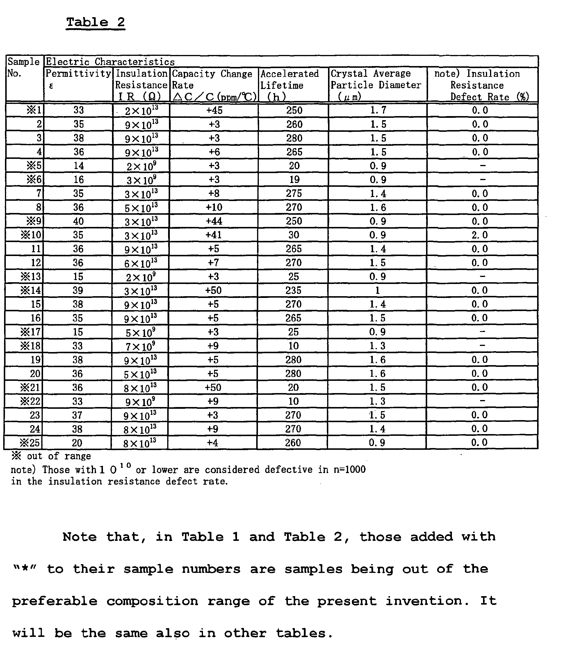
As shown in Table 1 and Table 2, by comparing the
sample numbers 1 to 5, it was confirmed that when 0.5 ≤ x
< 1 and preferably 0.6 ≤ x ≤ 0.9 was satisfied in the
main component including a dielectric oxide having a
composition expressed by [(CaxSr1-x)O]m[(TiyZr1-y-zHfz)O2],
the permittivity and insulation resistance were high, the
capacity change rate was small, the accelerated lifetime
was long, the average particle diameter of the crystal
was small and the insulation resistance defect rate was
low.
Also, as shown in Table 1 and Table 2, by comparing
the sample numbers 6 to 9, it was confirmed that when
0.01 ≤ y ≤ 0.10 and preferably 0.02 ≤ y ≤ 0.07 was
satisfied in the main component including a dielectric
oxide having a composition expressed by [(CaxSr1-x)O]m[(TiyZr1-y-zHfz)O2],
the permittivity and insulation
resistance were high, the capacity change rate was small,
the accelerated lifetime was long, and the insulation
resistance defect rate was low.
Also, as shown in Table 1 and Table 2, by comparing
the sample numbers 10 to 13, it was confirmed that when 0
< z ≤ 0.20 and preferably 0 < z ≤ 0.10 was satisfied in
the main component including a dielectric oxide having a
composition expressed by [(CaxSr1-x)0]m[(TiyZr1-y-zHfz)O2],
the permittivity and insulation resistance were high, the
capacity change rate was small, the accelerated lifetime
was long, and the insulation resistance defect rate was
low.
Also, as shown in Table 1 and Table 2, by comparing
the sample numbers 14 to 17, it was confirmed that when
0.90 ≤ m ≤ 1.04 was satisfied in the main component
including a dielectric oxide having a composition
expressed by [(CaxSr1-x)O]m[(TiyZr1-y-zHfz)O2], the
permittivity and insulation resistance were high, the
capacity change rate was small, the accelerated lifetime
was long, and the insulation resistance defect rate was
low.
Also, as shown in Table 1 and Table 2, by comparing
the sample numbers 18 to 21, it was confirmed that when a
Mn oxide in terms of MnO was included by 0.2 to 5 mol%
and preferably 0.2 to 3 mol% with respect to 100 mol% of
the main component, the permittivity and insulation
resistance were high, the capacity change rate was small,
the accelerated lifetime was long, and the insulation
resistance defect rate was low.
Also, as shown in Table 1 and Table 2, by comparing
the sample numbers 22 to 25, it was confirmed that when
an Al oxide in terms of Al2O3 was included by 0.1 to 10
mol% and preferably 0.1 to 5 mol% with respect to 100
mol% of the main component, the permittivity and
insulation resistance were high, the capacity change rate
was small, the accelerated lifetime was long, and the
insulation resistance defect rate was low.
Furthermore, as is known by comparing FIG. 2B
showing an enlarged picture of a section of a capacitor
sample as an example corresponding to the sample number 3
and FIG. 2A showing an enlarged picture of a section of a
capacitor sample as a comparative example corresponding
to the sample number 10 shown in Table 1 and Table 2, it
was confirmed that the average crystal particle diameter
became small by adding Hf in the main component.
Also, by comparing a curve B of the shrinkage (TMA)
curve at sintering shown in FIG. 3 of the capacitor
sample as an example corresponding to the sample number 3
with a curve A of the TMTA curve at sintering shown in
FIG. 3 of the capacitor sample as a comparative example
corresponding to the sample number 10 shown in Table 1
and Table 2, the fact below was also proved. Namely, by
adding Hf in the main component, the shrinkage curve at
sintering becomes gentle comparing with that of a
composition without Hf, and cracks and delamination are
hard to be caused at cofiring with internal electrodes.
Also, by adding Hf to the main component, crystal grain
growth can be suppressed and a finer and uniform crystal
can be realized comparing with that in the case of a
composition without Hf. This also agrees with the results
shown in FIG. 2.
As a result, according to the present invention, it
is considered that unevenness of insulation resistance
caused by unevenness of a boundary face due to cracks,
delamination or uneven crystal can be suppressed. This is
also obvious from the results shown in Table 1 and Table
2.
Other than weighing the materials, so that a
composition after firing would be the composition shown
in Table 3 below, capacitor samples were produced in the
same way as in the example 1, and the same evaluation was
made as that in the example 1. The results are shown in
Table 4.
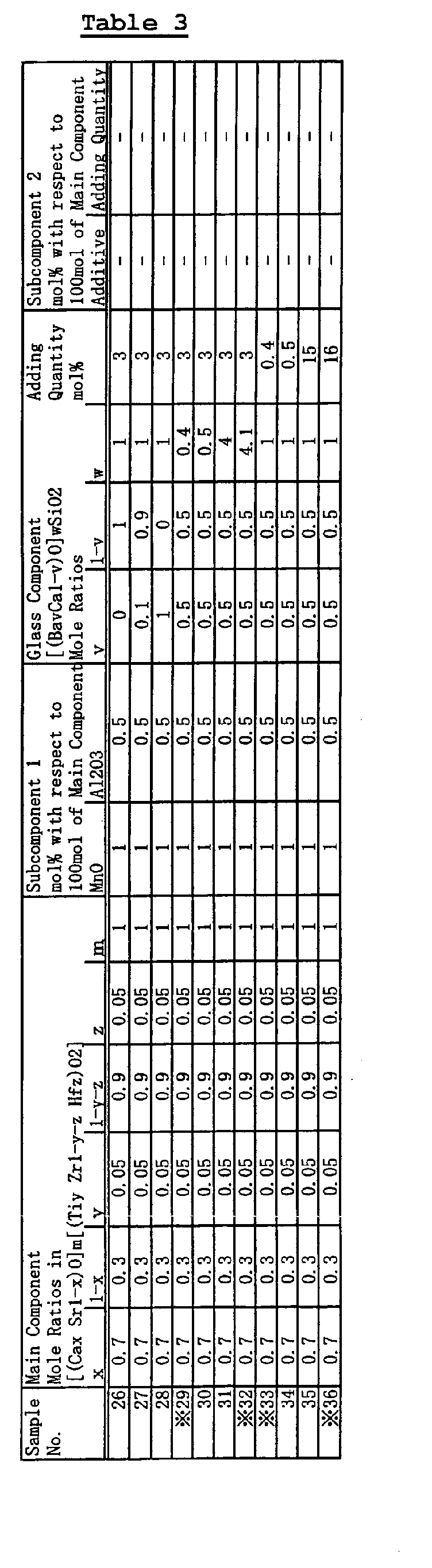
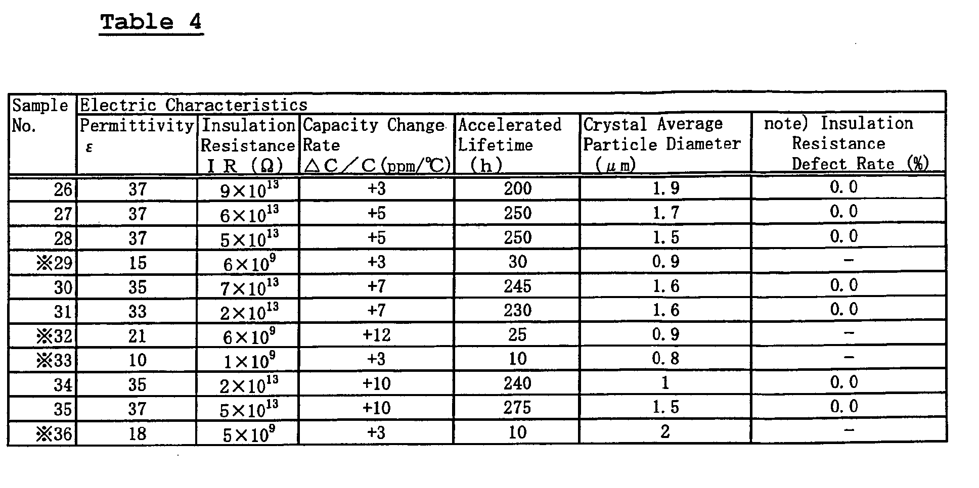
As shown in Table 3 and Table 4, by comparing the
sample numbers 26 to 28, it was confirmed that when a
range of 0 ≤ v ≤ 1 was satisfied in [(BavCa1-v)O]wSiO2 as a
preferable glass component to be added to the main
component, the permittivity and insulation resistance
were high, the capacity change rate was small, the
accelerated lifetime was long and the insulation
resistance defect rate was low.
Also, as shown in Table 3 and Table 4, by comparing
the sample numbers 29 to 32, it was confirmed that when a
range of 0.5 ≤ w ≤ 4.0 was satisfied in [(BavCa1-v)O]wSiO2
as a preferable glass component to be added to the main
component, the permittivity and insulation resistance
were high, the capacity change rate was small, the
accelerated lifetime was long and the insulation
resistance defect rate was low.
Also, as shown in Table 3 and Table 4, by comparing
the sample numbers 33 to 36, it was confirmed that when
0.5 to 15 mol% of a glass component was included with
respect to 100 mol% of the main component, the
permittivity and insulation resistance were high, the
capacity change rate was small, the accelerated lifetime
was long and the insulation resistance defect rate was
low.
Other than weighing the materials, so that a
composition after firing would be the composition shown
in Table 5 below, capacitor samples were produced in the
same way as in the example 1, and the same evaluation was
made as that in the example 1. The results are shown in
Table 6.

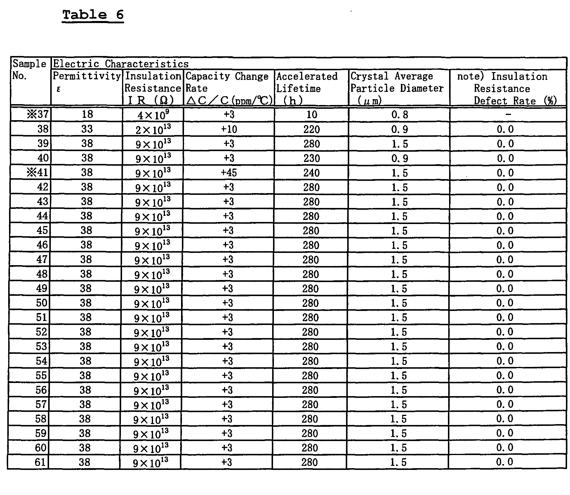
As shown in Table 5 and Table 6, by comparing the
sample numbers 37 to 41, it was confirmed that when Mg is
included by 0.02 to 1.5 mol% and preferably 0.10 to 1.0
mol% with respect to 100 mol% of the main component, the
permittivity and insulation resistance were high, the
capacity change rate was small, the accelerated lifetime
was long and the insulation resistance defect rate was
low.
Also, as shown in Table 5 and Table 6, by comparing
the sample numbers 37 to 61, it was confirmed that even
when at least one of Nb, Mo, Ta and W or at least one of
rare earth elements including Sc and Y is included (when
including at least one of Sc, Y, La, Ce, Pr, Nd, Sm, Eu,
Gd, Tb, Dy, Ho, Er, Tm, Yb and Lu) instead of Mg, the
equivalent effects to those in the case of including Mg
were confirmed to be obtained.
Other than weighing the materials, so that a
composition after firing would be the composition shown
in Table 7 below, capacitor samples were produced in the
same way as in the example 1, and the same evaluation was
made as that in the example 1. The results are shown in
Table 8.

| Sample No. | Electric Characteristics | |||||
| Permittivity ε | Insulation Resistance I R (Ω) | Capacity Change Rate ΔC / C (ppm/°C) | Accelerated Lifetime (h) | Crystal Average Particle Diameter (µm) | note) Insulation Resistance Defect Rate (%) | |
| 62 | 38 | 9 × 10¹³ | +3 | 280 | 1. 5 | 0.0 |
| 63 | 39 | 1 × 10¹⁴ | +2 | 290 | 1. 1 | 0.0 |
| 64 | 42 | 3 × 10¹⁴ | +1 | 305 | 0.8 | 0.0 |
| 65 | 39 | 1×10¹⁴ | +2 | 290 | 1. 1 | 0.0 |
| 66 | 38 | 9 × 10¹³ | +3 | 280 | 1. 5 | 0.0 |
As shown in Table 7 and Table 8, by comparing
sample numbers 62 to 66, it was confirmed that
particularly when 1.005 ≤ m ≤ 1.025 was satisfied in the
main component including a dielectric oxide having a
composition expressed by [(CaxSr1-x)O]m[(TiyZr1-y-zHfz)O2],
the permittivity and insulation resistance were
furthermore higher, the capacity change rate was
furthermore smaller, the accelerated lifetime was
furthermore longer, an average particle diameter of the
crystal was small and the insulation resistance defect
rate was low.
Other than weighing the materials, so that a
composition after firing would be the composition shown
in Table 9 below, capacitor samples were produced in the
same way as in the example 1, and the same evaluation was
made as that in the example 1. The results are shown in
Table 9.


As shown in Table 9 and Table 10, by comparing the
sample numbers 3 and 67 to 69, it was confirmed that when
a V oxide was included by 0 to 2.5 mol% and preferably
0.5 to 2.5 mol%, the permittivity and insulation
resistance were high, the capacity change rate was small,
the accelerated lifetime was long and the insulation
resistance defect rate was low. Particularly, when a V
oxide was included by 0.5 to 2.5 mol%, the accelerated
lifetime exhibited preferable results.
Other than changing the main firing temperature in
a range of 1220 to 1330°C as shown in Table 11 in the
composition of the sample number 3 in the example 1,
capacitor samples were produced in the same way as in the
example 1 and an evaluation was made in the same way as
in the example 1. The results are shown in Table 11. Note
that, in the present embodiment, dielectric loss (tanδ)
of the capacitor samples was also measured by an LCR
meter under a condition of 140°C and 20 Hz. Also, the
results of measuring temperature dependency by tanδ in
the capacitor samples are shown in FIG. 4B.


Capacitor samples were produced in the same way as
in the sample numbers 70 to 72 in the example 6 other
than collectively fabricating a dielectric paste not by
the solid-phase method but by the liquid-phase method,
and in the same way as in the example 6 other than
performing main firing at a temperature of 1220 to 1300°C.
An evaluation was made in the same way as in the example
6. The results are shown in Table 12. Also, results of
measuring temperature dependency by tanδ of the capacitor
samples are shown in FIG. 4A.
As shown in Table 11, in the present embodiment,
since sintering is sufficiently attained at a temperature
of 1300°C or lower, it was confirmed that it was possible
to be applied to the case of thinner layers.
Also, as is understood by comparing Table 11 with
Table 12 and FIG. 4B with FIG. 4A, it was confirmed that,
by producing the dielectric paste not by the liquid-phase
method but by the solid-phase method, it was possible to
improve the permittivity and insulation resistance, make
the capacity change rate small, improve the accelerated
lifetime, and reduce tanδ at 140°C.
Other than collectively fabricating a dielectric
paste having a composition of the sample number 10 (Hf is
not added) in the example 1 not by the solid-phase method
but by the liquid-phase method, capacitor samples were
produced in the same way as in the case of the sample
number 10 in the example 1 and an evaluation was made in
the same way as in the example 1. The results are shown
in Table 13. Note that, in the present embodiment, X-ray
analysis was also performed on dielectric layers of the
capacitor samples, and a CV value (variation coefficient)
indicating dispersibility of respective elements in the
dielectric layers was also measured as shown in Table 13.
The CV value is defined as a value obtained by
calculating standard deviation D(x) from an X-ray
intensity distribution of each element in the dielectric
layer and dividing the standard deviation D(x) by an
expectation value E(x) of the X-ray intensity
distribution of each element. When the CV value is small,
the dispersibility is preferable.
The CV value (variation coefficient) indicating
dispersibility of each element in the dielectric layer
was measured on capacitor samples having a composition of
the sample number 3 (Hf is added) in the example 1 in the
same way as in the reference example 2. The results are
shown in Table 13.

In Table 13, as is known by comparing the sample
number 77 with the sample number 3, by adding Hf (the
sample number 3) to the main component, moreover, by
applying the solid-phase method instead of the liquid-phase
method (the sample number 77), it was confirmed
that dispersibility of respective elements (Ca, Sr, Ti,
Zr, Ba, Si, Mn and Al) improved. Also, in the sample
number 3 as an example, the insulation resistance and
accelerated lifetime were improved and the insulation
resistance defect rate was reduced.
As explained above, according to the present
invention, it is possible to realize a highly reliable
nonreducing dielectric ceramic composition, preferably
used as a dielectric layer of a multilayer ceramic
capacitor, etc. using a base metal, such as Ni, as an
internal electrode and able to be sintered at 1300°C or
lower; wherein a temperature coefficient of the
capacitance is small and able to be freely controlled in
a range of -15 to +150 ppm/°C, the insulation resistance
at 25°C is 1×10¹³ Ω or higher, the specific permittivity
and dielectric loss tangent (tanδ) have a little
frequency dependency, accelerated lifetime of the
insulation resistance is long, and a insulation
resistance defect rate is low even when the insulation
layer is made thin.
Claims (14)
- A dielectric ceramic composition including at least
a main component containing a dielectric oxide having a composition expressed by [(CaxSr1-x)O]m[(TiyZr1-y-zHfz)O2],
a first subcomponent containing a Mn oxide and/or an Al oxide, and
a glass component:wherein "m", "x", "y" and "z" indicating composition mole ratios in the formula included in said main component are in relationships of
0.90 ≤ m ≤ 1.04
0.5 ≤ x < 1
0.01 ≤ y ≤ 0.10
0 < z ≤ 0.20. - The dielectric ceramic composition as set forth in claim 1, including 0.2 to 5 mol% of said Mn oxide in terms of MnO and 0.1 to 10 mol% of said Al oxide in terms of Al2O3 with respect to 100 mol% of said main component.
- The dielectric ceramic composition as set forth in claim 1 or 2, including 0 to 2.5 mol% (note that 0 is excluded) of a V oxide in terms of V2O5 with respect to 100 mol% of said main component.
- The dielectric ceramic composition as set forth in any one of claims 1 to 3, wherein said glass component contains at least SiO2 as a main component.
- The dielectric ceramic composition as set forth in any one of claims 1 to 4, wherein said glass component is expressed by [(BavCa1-v)O]wSiO2, "v" and "w" in the composition formula of said glass component are in ranges of 0 ≤ v ≤ 1 and 0.5 ≤ w ≤ 4.0, and said glass component is included by 0.5 to 15 mol% with respect to 100 mol% of said main component.
- The dielectric ceramic composition as set forth in any one of claims 1 to 5, including at least one of rare earth elements including Sc and Y by 0.02 to 1.5 mol% with respect to 100 mol% of said main component.
- The dielectric ceramic composition as set forth in any one of claims 1 to 6, including at least one of Nb, Mo, Ta, W and Mg by 0.02 to 1.5 mol% with respect to 100 mol% of said main component.
- The dielectric ceramic composition as set forth in any one of claims 1 to 7, wherein "m" indicating a composition mole ratio in the formula contained in said main component is 1.005 ≤ m ≤ 1.025.
- A production method of the dielectric ceramic composition as set forth in any one of claims 1 to 8, comprising the steps of:preparing materials of said dielectric ceramic composition;mixing said materials;obtaining a calcinated substance by collectively calcinating said mixed materials to bring solid-phase reaction by using a dry synthesis method; andobtaining said dielectric ceramic composition by performing main firing on said calcinated substance.
- An electronic device having a dielectric layer:wherein said dielectric layer is composed of the dielectric ceramic composition as set forth in any one of claims 1 to 8.
- An electronic device having alternately stacked internal electrodes and dielectric layers,
wherein said dielectric layers are composed of the dielectric ceramic composition as set forth in any one of claims 1 to 8. - The electronic device as set forth in claim 11, wherein said internal electrode includes at least nickel.
- The electronic device as set forth in claim 11 or 12, wherein an average particle diameter of a crystal in said dielectric layer is 2 µm or less.
- A production method of the electronic device as set forth in any one of claims 11 to 13, wherein main firing at 1300°C or lower is performed on said internal electrodes and dielectric layers at a time.
Applications Claiming Priority (3)
| Application Number | Priority Date | Filing Date | Title |
|---|---|---|---|
| JP2002372783 | 2002-12-24 | ||
| JP2002372783 | 2002-12-24 | ||
| PCT/JP2003/016178 WO2004063119A1 (en) | 2002-12-24 | 2003-12-17 | Dielectric porcelain composition, electronic device and methods for producing these |
Publications (2)
| Publication Number | Publication Date |
|---|---|
| EP1580179A1 true EP1580179A1 (en) | 2005-09-28 |
| EP1580179A4 EP1580179A4 (en) | 2009-01-14 |
Family
ID=32708191
Family Applications (1)
| Application Number | Title | Priority Date | Filing Date |
|---|---|---|---|
| EP03780844A Withdrawn EP1580179A4 (en) | 2002-12-24 | 2003-12-17 | Dielectric porcelain composition, electronic device and methods for producing these |
Country Status (7)
| Country | Link |
|---|---|
| US (1) | US7312172B2 (en) |
| EP (1) | EP1580179A4 (en) |
| JP (1) | JP4548118B2 (en) |
| KR (1) | KR100673878B1 (en) |
| CN (1) | CN1313418C (en) |
| TW (1) | TWI264426B (en) |
| WO (1) | WO2004063119A1 (en) |
Cited By (1)
| Publication number | Priority date | Publication date | Assignee | Title |
|---|---|---|---|---|
| EP4211092A4 (en) * | 2020-09-10 | 2025-12-10 | Kemet Electronics Corp | DIELECTRIC CERAMIC COMPOSITION AND CERAMIC CAPACITOR SO THAT |
Families Citing this family (13)
| Publication number | Priority date | Publication date | Assignee | Title |
|---|---|---|---|---|
| CN101489952B (en) * | 2006-07-07 | 2013-05-01 | 株式会社村田制作所 | Dielectric ceramics, ceramic electronic components, and multilayer ceramic capacitors |
| JP4678022B2 (en) * | 2007-11-26 | 2011-04-27 | Tdk株式会社 | Method for producing dielectric ceramic composition |
| JP4561922B2 (en) * | 2008-03-31 | 2010-10-13 | Tdk株式会社 | DIELECTRIC CERAMIC COMPOSITION, ELECTRONIC COMPONENT AND METHOD FOR PRODUCING THEM |
| KR101115647B1 (en) * | 2008-03-31 | 2012-02-16 | 티디케이가부시기가이샤 | A dielectric ceramic composition, an electronic component and a manufacturing method thereof |
| US8178456B2 (en) * | 2008-07-08 | 2012-05-15 | Ian Burn Consulting, Inc. | Sintered dielectric ceramic, composition for making, and use thereof in multilayer capacitor and energy storage device |
| KR101113441B1 (en) * | 2009-12-31 | 2012-02-29 | 삼성전기주식회사 | Dielectric ceramic composition and multilayer ceramic capacitor comprising the same |
| JP6226078B2 (en) * | 2014-08-04 | 2017-11-08 | 株式会社村田製作所 | Multilayer ceramic capacitor |
| CN106356191B (en) * | 2015-07-17 | 2019-05-31 | 株式会社村田制作所 | Laminated ceramic capacitor, slurry and Ca-Ti ore type construction |
| KR102029529B1 (en) * | 2016-12-19 | 2019-10-07 | 삼성전기주식회사 | Multi-layered ceramic capacitor |
| JP7429516B2 (en) * | 2018-12-20 | 2024-02-08 | 株式会社日本触媒 | Ceramic sheet and its manufacturing method |
| CN114262227A (en) * | 2021-11-26 | 2022-04-01 | 西安交通大学 | Method for improving dielectric nonlinear dielectricity of barium titanate ceramic by equivalent-acceptor doping |
| CN115010488B (en) * | 2022-01-17 | 2023-04-14 | 北京元六鸿远电子科技股份有限公司 | Low-firing low-dielectric high-Q high-stability microwave porcelain for capacitor |
| JP7847477B2 (en) * | 2022-05-30 | 2026-04-17 | Tdk株式会社 | Dielectric compositions and multilayer ceramic electronic components |
Family Cites Families (15)
| Publication number | Priority date | Publication date | Assignee | Title |
|---|---|---|---|---|
| JPH0831284B2 (en) * | 1986-11-14 | 1996-03-27 | 株式会社村田製作所 | Dielectric ceramic composition for non-reducing temperature compensation |
| US5319517A (en) * | 1992-03-27 | 1994-06-07 | Tdk Corporation | Multilayer ceramic chip capacitor |
| JP3134024B2 (en) | 1993-03-22 | 2001-02-13 | ティーディーケイ株式会社 | Multilayer ceramic chip capacitors |
| JPH0818866B2 (en) * | 1994-03-25 | 1996-02-28 | 堺化学工業株式会社 | Ceramic dielectric composition |
| JPH10101417A (en) * | 1996-09-25 | 1998-04-21 | Sakai Chem Ind Co Ltd | Dielectric porcelain and composition for producing dielectric porcelain |
| JP2997236B2 (en) | 1997-03-31 | 2000-01-11 | ティーディーケイ株式会社 | Non-reducing dielectric porcelain material |
| WO1998044523A1 (en) * | 1997-03-31 | 1998-10-08 | Tdk Corporation | Non-reducing dielectric ceramic material |
| JP2001097772A (en) | 1999-09-30 | 2001-04-10 | Tdk Corp | Dielectric porcelain composition, electronic part and method for producing the same |
| JP3520053B2 (en) | 2000-02-09 | 2004-04-19 | Tdk株式会社 | Dielectric porcelain composition, electronic component and method for producing electronic component |
| JP2001220229A (en) * | 2000-02-09 | 2001-08-14 | Tdk Corp | Dielectric ceramic composition, electronic part and method for producing electronic part |
| JP3470703B2 (en) * | 2000-04-07 | 2003-11-25 | 株式会社村田製作所 | Non-reducing dielectric ceramic, multilayer ceramic capacitor using the same, and method for producing non-reducing dielectric ceramic |
| JP3503568B2 (en) * | 2000-04-07 | 2004-03-08 | 株式会社村田製作所 | Non-reducing dielectric ceramic and multilayer ceramic capacitor using the same |
| EP1216974A1 (en) * | 2000-12-20 | 2002-06-26 | Matsushita Electric Industrial Co., Ltd. | Dielectric ceramic-glass composite and dielectric device |
| JP3705141B2 (en) * | 2001-03-19 | 2005-10-12 | 株式会社村田製作所 | Dielectric ceramic, manufacturing method and evaluation method thereof, and multilayer ceramic electronic component |
| JP4506084B2 (en) * | 2002-04-16 | 2010-07-21 | 株式会社村田製作所 | Non-reducing dielectric ceramic, method for manufacturing the same, and multilayer ceramic capacitor |
-
2003
- 2003-12-17 WO PCT/JP2003/016178 patent/WO2004063119A1/en not_active Ceased
- 2003-12-17 EP EP03780844A patent/EP1580179A4/en not_active Withdrawn
- 2003-12-17 CN CNB2003801099512A patent/CN1313418C/en not_active Expired - Lifetime
- 2003-12-17 KR KR1020057011871A patent/KR100673878B1/en not_active Expired - Lifetime
- 2003-12-17 JP JP2004566289A patent/JP4548118B2/en not_active Expired - Lifetime
- 2003-12-17 US US10/540,395 patent/US7312172B2/en not_active Expired - Lifetime
- 2003-12-19 TW TW092136127A patent/TWI264426B/en not_active IP Right Cessation
Cited By (1)
| Publication number | Priority date | Publication date | Assignee | Title |
|---|---|---|---|---|
| EP4211092A4 (en) * | 2020-09-10 | 2025-12-10 | Kemet Electronics Corp | DIELECTRIC CERAMIC COMPOSITION AND CERAMIC CAPACITOR SO THAT |
Also Published As
| Publication number | Publication date |
|---|---|
| TWI264426B (en) | 2006-10-21 |
| CN1753847A (en) | 2006-03-29 |
| US20060234853A1 (en) | 2006-10-19 |
| EP1580179A4 (en) | 2009-01-14 |
| KR20050093799A (en) | 2005-09-23 |
| TW200418743A (en) | 2004-10-01 |
| JPWO2004063119A1 (en) | 2006-05-18 |
| CN1313418C (en) | 2007-05-02 |
| JP4548118B2 (en) | 2010-09-22 |
| KR100673878B1 (en) | 2007-01-25 |
| HK1087393A1 (en) | 2006-10-13 |
| WO2004063119A1 (en) | 2004-07-29 |
| US7312172B2 (en) | 2007-12-25 |
Similar Documents
| Publication | Publication Date | Title |
|---|---|---|
| US7176156B2 (en) | Electronic device, dielectric ceramic composition and the production method | |
| US7042707B2 (en) | Multilayer ceramic capacitor | |
| US7678724B2 (en) | Electronic device, dielectric ceramic composition and the production method | |
| EP1648004B1 (en) | Dielectric ceramic composition with dielectric core-shell particles and electronic device | |
| EP1826190A2 (en) | Dielectric ceramic composition and the production method | |
| US7696118B2 (en) | Dielectric ceramic composition, electronic device and the production method | |
| EP1820784A1 (en) | Electronic device, dielectric ceramic composition and the production method | |
| US20070223177A1 (en) | Multilayer electronic device and the production method | |
| US7550402B2 (en) | Ceramic electronic device and the production method | |
| EP1138652A1 (en) | Method of producing ceramic composition and method of producing electronic device | |
| EP1683769B1 (en) | Electronic device, dielectric ceramic composition and the production method | |
| EP1916681B1 (en) | Dielectric ceramic composition and electronic device | |
| US7312172B2 (en) | Dielectric ceramic composition, electronic device and production methods of the same | |
| EP1298105B1 (en) | Dielectrics porcelain composition and electronic parts | |
| US20090246541A1 (en) | Dielectric ceramic composition, an electric component and a manufacturing method thereof | |
| US7265072B2 (en) | Dielectric ceramic composition and electronic device | |
| US7518849B2 (en) | Multilayer electronic device and the production method | |
| EP1826191A2 (en) | Dielectric ceramic composition, electronic device and the production method | |
| US7399724B2 (en) | Electronic device, dielectric ceramic composition and production method of the same | |
| JP2000260653A (en) | Multilayer ceramic capacitor and inspection method thereof |
Legal Events
| Date | Code | Title | Description |
|---|---|---|---|
| PUAI | Public reference made under article 153(3) epc to a published international application that has entered the european phase |
Free format text: ORIGINAL CODE: 0009012 |
|
| 17P | Request for examination filed |
Effective date: 20050630 |
|
| AK | Designated contracting states |
Kind code of ref document: A1 Designated state(s): AT BE BG CH CY CZ DE DK EE ES FI FR GB GR HU IE IT LI LU MC NL PT RO SE SI SK TR |
|
| RBV | Designated contracting states (corrected) |
Designated state(s): DE FR GB |
|
| A4 | Supplementary search report drawn up and despatched |
Effective date: 20081211 |
|
| 17Q | First examination report despatched |
Effective date: 20120316 |
|
| STAA | Information on the status of an ep patent application or granted ep patent |
Free format text: STATUS: THE APPLICATION IS DEEMED TO BE WITHDRAWN |
|
| 18D | Application deemed to be withdrawn |
Effective date: 20120727 |