EP1579732B1 - Sensing light emitted from multiple light sources - Google Patents
Sensing light emitted from multiple light sources Download PDFInfo
- Publication number
- EP1579732B1 EP1579732B1 EP03777092.2A EP03777092A EP1579732B1 EP 1579732 B1 EP1579732 B1 EP 1579732B1 EP 03777092 A EP03777092 A EP 03777092A EP 1579732 B1 EP1579732 B1 EP 1579732B1
- Authority
- EP
- European Patent Office
- Prior art keywords
- signal
- light
- lock
- photodetector
- led
- Prior art date
- Legal status (The legal status is an assumption and is not a legal conclusion. Google has not performed a legal analysis and makes no representation as to the accuracy of the status listed.)
- Expired - Lifetime
Links
- 101100537098 Mus musculus Alyref gene Proteins 0.000 claims description 19
- 101150095908 apex1 gene Proteins 0.000 claims description 19
- 101100269674 Mus musculus Alyref2 gene Proteins 0.000 claims description 15
- 238000001228 spectrum Methods 0.000 claims description 10
- 238000005286 illumination Methods 0.000 claims description 4
- 238000000034 method Methods 0.000 description 14
- 238000010586 diagram Methods 0.000 description 10
- 102100024061 Integrator complex subunit 1 Human genes 0.000 description 9
- 101710092857 Integrator complex subunit 1 Proteins 0.000 description 9
- 102100033265 Integrator complex subunit 2 Human genes 0.000 description 9
- 108050002021 Integrator complex subunit 2 Proteins 0.000 description 9
- 238000004519 manufacturing process Methods 0.000 description 9
- 230000003595 spectral effect Effects 0.000 description 6
- 101100412102 Haemophilus influenzae (strain ATCC 51907 / DSM 11121 / KW20 / Rd) rec2 gene Proteins 0.000 description 3
- 101100356020 Haemophilus influenzae (strain ATCC 51907 / DSM 11121 / KW20 / Rd) recA gene Proteins 0.000 description 3
- 101100042680 Mus musculus Slc7a1 gene Proteins 0.000 description 3
- XUIMIQQOPSSXEZ-UHFFFAOYSA-N Silicon Chemical compound [Si] XUIMIQQOPSSXEZ-UHFFFAOYSA-N 0.000 description 3
- 230000005693 optoelectronics Effects 0.000 description 3
- 229910052710 silicon Inorganic materials 0.000 description 3
- 239000010703 silicon Substances 0.000 description 3
- 102100033263 Integrator complex subunit 3 Human genes 0.000 description 2
- 101710092886 Integrator complex subunit 3 Proteins 0.000 description 2
- 230000008901 benefit Effects 0.000 description 2
- 230000008878 coupling Effects 0.000 description 2
- 238000010168 coupling process Methods 0.000 description 2
- 238000005859 coupling reaction Methods 0.000 description 2
- 238000012986 modification Methods 0.000 description 2
- 230000004048 modification Effects 0.000 description 2
- 230000003287 optical effect Effects 0.000 description 2
- OAICVXFJPJFONN-UHFFFAOYSA-N Phosphorus Chemical compound [P] OAICVXFJPJFONN-UHFFFAOYSA-N 0.000 description 1
- 239000003795 chemical substances by application Substances 0.000 description 1
- 238000001914 filtration Methods 0.000 description 1
- 239000000463 material Substances 0.000 description 1
- 238000005259 measurement Methods 0.000 description 1
- 239000004065 semiconductor Substances 0.000 description 1
- 238000006467 substitution reaction Methods 0.000 description 1
- 238000001429 visible spectrum Methods 0.000 description 1
Images


Classifications
-
- H—ELECTRICITY
- H05—ELECTRIC TECHNIQUES NOT OTHERWISE PROVIDED FOR
- H05B—ELECTRIC HEATING; ELECTRIC LIGHT SOURCES NOT OTHERWISE PROVIDED FOR; CIRCUIT ARRANGEMENTS FOR ELECTRIC LIGHT SOURCES, IN GENERAL
- H05B45/00—Circuit arrangements for operating light-emitting diodes [LED]
- H05B45/20—Controlling the colour of the light
- H05B45/22—Controlling the colour of the light using optical feedback
-
- H—ELECTRICITY
- H05—ELECTRIC TECHNIQUES NOT OTHERWISE PROVIDED FOR
- H05B—ELECTRIC HEATING; ELECTRIC LIGHT SOURCES NOT OTHERWISE PROVIDED FOR; CIRCUIT ARRANGEMENTS FOR ELECTRIC LIGHT SOURCES, IN GENERAL
- H05B45/00—Circuit arrangements for operating light-emitting diodes [LED]
- H05B45/10—Controlling the intensity of the light
- H05B45/12—Controlling the intensity of the light using optical feedback
-
- H—ELECTRICITY
- H05—ELECTRIC TECHNIQUES NOT OTHERWISE PROVIDED FOR
- H05B—ELECTRIC HEATING; ELECTRIC LIGHT SOURCES NOT OTHERWISE PROVIDED FOR; CIRCUIT ARRANGEMENTS FOR ELECTRIC LIGHT SOURCES, IN GENERAL
- H05B45/00—Circuit arrangements for operating light-emitting diodes [LED]
- H05B45/30—Driver circuits
- H05B45/305—Frequency-control circuits
Definitions
- the technical field of this disclosure is light production from light emitting diodes (LEDs), particularly, sensing light emitted simultaneously from multiple light sources.
- LEDs light emitting diodes
- Illumination sources such as lamps, currently utilize incandescent and fluorescent means as light production. It is well known that incandescent light sources are inefficient light sources that utilize more power resources than other light sources. Fluorescent light sources have provided a more efficient light production.
- LEDs Light emitting diodes
- Producing usable light with LEDs generally requires either manufacturing an LED that produces a specified color, such as utilizing a phosphor layer overlying the LED, or mixing a plurality of colored LEDs to produce a desired colored light output. Unfortunately, once a light source package is produced to achieve the desired colored light output its useful life is reduced to the amount of time until a failure or partial failure of one of its component parts occurs.
- LED characteristics depend on temperature, drive current, and time. Additionally, LED characteristics vary from LED to LED. Although an LED-based lamp may be set to operate at a given color point and intensity, at the beginning of its life, the actual color and intensity obtained at that setting may not remain constant.
- Mixing a plurality of colored light sources may include a control system that varies individual light source contributions to correct for variation in the LED characteristics That is, as the output of component LEDs varies, the control system can maintain a desired spectral output and intensity by varying individual LED output to compensate for the variations.
- sensing systems for controlling a specified colored light output include temperature feed-forward or intensity feedback systems containing a single unfiltered photodiode.
- Another sensing system includes utilizing multiple photodiodes, for example three or more, and corresponding color filters. This system may be referred to as a color filter photodiode control system.
- this system can be implemented utilizing a time-based approach whereby the LEDs are pulsed on and off in a particular pattern allowing the sensing of the intensity of the independent LED groups.
- An advantage of the color filter photodiode control system over the temperature feed-forward or intensity feedback systems is that the color filter photodiode control system can sense the average levels of the different spectral outputs of the LEDs, for example red, green, and blue, without having to turn the LEDs on and off in a particular pattern. Additionally, a low pass filter can be used to integrate the signal from each LED group. The accuracy of this method is strongly influenced by the color filters on the photodiodes.
- temperature feed-forward or intensity feedback systems require that LEDs be turned on and off briefly to permit sensing of the individual color components, for example red, green and blue.
- This approach is susceptible to errors resulting from ripple in the driving current, and changes in the drive waveform, such as, for example changes in the rise and fall times of the LED drive current pulses.
- the color filter photodiode control system although not requiring the turning on and off of LEDs to sense the individual color components, does require more expensive sensors containing color filters as well as a larger total number of sensors. None of the systems corrects for ambient light.
- US 6 055 251 A discloses a semiconductor laser control system comprising a control unit for producing a drive signal and a reference signal, a plurality of colored light sources designed to receive the drive signal from an associated control unit and to produce a light signal based on the drive signal, wherein each light source emits a light signal at a discrete frequency and a reference signal at a discrete frequency, a photodetector optically coupled to the plurality of light sources and designed to receive the light signals from the plurality of light sources, and to produce a received light signal, and a lock-in system coupled to the photodectector and each light source, the lock-in system receiving the received light signal from the photodetector and receiving the reference signal from an associated control unit, wherein the lock-in system produces an intensity value of the associated light source based on the received light signal and the reference signal.
- the present invention is directed to a light source control system for an illumination source.
- the invention provides for a frequency sensing structure that produces an intensity value input for a control system.
- the invention provides a light source control system according to claim 1.
- connection means a direct physical or optical connection between the things that are connected, without any intermediate devices.
- coupled means either a direct physical or optical connection between the things that are connected or an indirect connection through one or more passive or active intermediary devices.
- circuit means either a single component or a multiplicity of components, either active or passive, that are coupled together to perform a desired function.
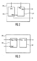
- FIG. 1 is a schematic diagram illustrating a sensing device 100 according to an embodiment of the present invention.
- Device structure 100 includes control units (110, 120, and 130), light emitting diodes (115, 125 and 135), a photodetector 150, and lock-in systems (170, 180, and 190).
- LEDs light emitting diodes
- each LED represents a block of independently-driven LEDs with a substantially similar spectral light output.
- LED 115 may consist of several LEDs, all emitting a red light output.
- LED 125 may include all green light emitting LEDs
- LED 135 may include all blue light emitting LEDs.
- the present invention is implemented as a single LED or a single color group of LEDs, a single control unit, and a single lock-in unit in addition to the photodetector.
- sensing device 100 is implemented as a plurality of LEDs or multi-color LED groups, each independently-driven LED or LED group having an associated control unit and an associated lock-in system.
- emitted spectra of the LEDs form a multi-source light signal. For example, a red, a green, and a blue LED or groups of LEDs are utilized to produce a "white" multi-source light signal.
- Each control unit (110, 120, and 130), detailed in FIG. 2 below, includes an associated output drive signal terminal (Drv1, Drv2, and Drv3) and an associated output reference terminal (Ref1, Ref2, and Ref3).
- Each output drive signal terminal (Drv1, Drv2, and Drv3) is coupled to an associated light emitting diode (115, 125 and 135).
- output drive signal terminal (Drv1) is coupled to light emitting diodes (115)
- output drive signal terminal (Drv2) is coupled to light emitting diode (125)
- output drive signal terminal (Drv3) is coupled to light emitting diode (135).
- Light emitting diodes (115, 125 and 135) are optoelectronic devices that produce light when power is supplied causing them to forward bias.
- the light produced may be within the blue, green, red, amber or other portion of the spectrum, depending on the material utilized in manufacturing the LED.
- LEDs (115, 125 and 135) are implemented as LXHL-BM01, LXHL-BB01 and LXHL-BD01 available from Lumileds corporation of San Jose, CA.
- LEDs (115, 125 and 135) are implemented as NSPB300A, NSPG300A and NSPR800AS from Nichia corporation of Mountville, PA.
- Each control unit produces a drive signal and a reference signal, as detailed in FIG. 2 below.
- Power in the form of the drive signal, is transmitted to the associated light emitting diode (LED) or LED group and the reference signal is transmitted to the associated lock-in unit.
- the LED receives the drive signal and produces a light signal based on the drive signal.
- the drive signal is generated at a discrete frequency.
- the reference signal is transmitted to the associated lock-in system and includes the same discrete frequency.
- Multiple control units and associated LEDs produce a light signal including several intensity values representing the intensity of light emitted by each LED or LED group.
- the frequency of the drive signals ranges from about 400 Hz to about 1.2 kHz while the frequency of the light emitted from the LEDs or LED groups is in the order of 10 14 Hz.
- Photodetector 150 is an optoelectronic device that responds to light signals and produces a received light signal.
- photodetector 150 is implemented as a photodiode, such as, for example PS 1-2CH from Pacific Silicon Sensor, Inc of Westlake Village, CA.
- Photodetector 150 includes an output signal terminal (Rec) for supplying the received light signal.
- photodetector 150 responds to a single source light signal and produces a received light signal, at the output signal terminal (Rec), which corresponds to the intensity of light produced by that single light source.
- photodetector 150 responds to the multi-source light signal and produces a received light signal, at the output signal terminal (Rec).
- the received light signal includes components at multiple frequencies, each component corresponding to the intensity of one light source in the multi-source light signal.
- Each lock-in system (170, 180, and 190) includes a lock-in device, detailed in FIG. 3 below.
- Each lock-in system (170, 180, and 190) further includes an input signal terminal (Rec) and an associated input reference terminal (Ref1, Ref2, and Ref3).
- Each input signal terminal (Rec) of each associated lock-in system (170, 180, and 190) is coupled to the output signal terminal (Rec) of photodetector 150.
- Each input reference terminal (Ref1, Ref2, and Ref3) of each associated lock-in system (170, 180, and 190) is coupled to the output reference terminal (Ref1, Ref2, and Ref3) of each associated control unit (110, 120, and 130).
- output reference terminal (Ref1) of control unit 110 is coupled to input reference terminal (Ref1) of lock-in system 170
- output reference terminal (Ref2) of control unit 120 is coupled to input reference terminal (Ref1) of lock-in system 180
- output reference terminal (Ref3) of control unit 130 is coupled to input reference terminal (Ref3) of lock-in system 190.
- Each lock-in system (170, 180, and 190) further includes an associated output intensity signal terminal (Int1, Int2, and Int3), detailed in FIG. 3 below.
- Each lock-in system receives an input signal, at the input signal terminal (Rec), from photodetector 150 and a reference signal, at the input reference terminal (Ref1, Ref2, and Ref3), from an associated control unit (110, 120, and 130).
- Each lock-in system produces an output intensity signal, at the associated output intensity signal terminal (Int1, Int2, and Int3), based on the received input signal and reference signal.
- sensing device 100 includes a high-pass filter coupled between the output reference terminal (Ref1, Ref2, and Ref3) of each control unit (110, 120, and 130) and the input reference terminal (Ref1, Ref2, and Ref3) of the associated lock-in system (170, 180, and 190).
- coupling a high-pass filter between the control unit and the lock-in system reduces spurious dc components from affecting the reference signal.
- FIG. 2 is a schematic diagram illustrating a control unit 210 according to an embodiment of the present invention.
- Control unit 210 includes a frequency shifter 215, a power distributor 217, an input clock signal terminal (Clk), an input power signal terminal (Pwr), an output reference signal terminal (Ref), and an output drive signal terminal.
- Control unit 210 receives a clock signal and a power signal, produces a reference signal based on the clock signal, and produces a drive signal based on the reference signal and the power signal.
- Frequency shifter 215 includes an input clock signal terminal (Clk) and an output reference signal terminal (Ref). Frequency shifter 215 receives the clock signal and produces the reference signal based on the clock signal. In one embodiment, frequency shifter 215 receives the clock signal and "divides down" the clock signal to produce the reference signal. The reference signal frequency utilized is produced at a frequency so as not to cause noticeable "flicker" to the human eye. In an example, a reference signal is produced in the 100 Hz - 2.4 kHz range.
- frequency shifter 215 includes an internal clock that generates the clock signal internally thereby eliminating the need for the clock terminal (Clk):
- control unit 110 produces a reference frequency at 400 Hz
- control unit 120 produces a reference frequency at 500 Hz
- control unit 130 produces a reference frequency at 600 Hz.
- Power distributor 217 includes an input power terminal (Pwr), an input reference signal terminal (Ref), and an output drive signal terminal (Drv).
- the input reference terminal (Ref) of power distributor 217 is coupled to the output reference terminal (Ref) of frequency shifter 215.
- Power distributor 217 receives the power signal and the reference signal and produces the drive signal based on the power signal and the reference signal.
- the power signal is implemented as a voltage source signal. In another embodiment, the power signal is implemented as a current source signal. In an example, power distributor 217 produces a drive signal including a current signal modulated at a discrete frequency associated with the reference signal.
- the power signal may be produced in the form of one of several different waveforms, such as, for example, a sine wave, a cosine wave, a square wave, or any other waveform that would allow the production of the light signal.
- FIG. 3 is a schematic diagram illustrating a lock-in device 370 according to an embodiment of the present invention.
- Lock-in device 370 includes a signal multiplier 375, a filter 377, an input signal terminal (Rec), an input reference terminal (Ref), and an output intensity terminal (Int).
- Lock-in device 370 receives an input signal and a reference signal, and produces an intensity signal based on the input signal and the reference signal.
- Signal multiplier 375 includes an input signal terminal (Rec), an input reference terminal (Ref), and an output product terminal (Prd). Signal multiplier 375 receives the input signal and the reference signal, and produces a product signal based on the input signal and the reference signal. Signal multiplier 375 produces the product signal by multiplying the input signal by the reference signal, detailed in FIG. 5 below. Signal multiplier 375 can be implemented as a signal multiplier chip, such as, for example the MLT04 produced by Analog Devices of Norwood, MA.
- Filter 377 includes an input product terminal (Prd) and an output intensity terminal (Int).
- the input product terminal (Prd) of filter 377 is coupled to the output product terminal (Prd) of signal multiplier 375.
- Filter 377 receives the product signal and filters the received product signal to remove non-dc portions of the signal.
- filter 377 is implemented as a low-pass filter.
- FIG. 4 is a schematic diagram illustrating a sensing device 400 according to another embodiment of the present invention.
- Device structure 400 includes control units (110, 120, and 130), light emitting diodes (115, 125 and 135), photodetectors 450 and 455, and lock-in systems (470, 480, and 490).
- control units 110, 120, and 130
- light emitting diodes 115, 125 and 135
- lock-in systems 470, 480, and 490.
- Like components from FIG.1 are numbered identically and function identically.
- implementation of the present invention allows any number of light emitting diodes (LEDs) to be utilized, so long as there is a corresponding control unit and lock-in system for each independently driven LED or group of LEDs.
- LEDs light emitting diodes
- Photodetectors 450 and 455 are optoelectronic devices that respond to light signals across the whole visible spectrum, and each produce a received light signal within a predetermined spectrum.
- photodetectors 450 and 455 are implemented as two separate single junction photodiodes, such as, for example PSS 1-2CH from Pacific Silicon Sensor, Inc.
- photodetector 450 includes an output signal terminal (Rec1) for supplying a portion of the received light signal
- photodetector 455 includes an output signal terminal (Rec2) for supplying another portion of the received light signal.
- photodetectors 450 and 455 are implemented as a multi-junction photodiode, such as, for example PSS-WS7.56 from Pacific Silicon Sensor, Inc.
- photodetector 450 represents a first junction of the multi-junction photodiode
- photodetector 455 represents a second junction of the multi-junction photodiode.
- One junction is more sensitive to red wavelengths, and the other is more sensitive to blue wavelengths. Comparison of the measurements of the two junctions provides a measure of spectral shift.
- photodetector 450 responds more strongly than photodetector 455 to light signals within the spectrum defined as greater than about 600nm. In this example, photodetector 455 responds most strongly than photodetector 450 to light signals within the spectrum defined as less than about 600nm.
- Photodetectors 450 and 455 respond to single and multi-source light signals and produce a received light signal, at the output signal terminals (Rec1 and Rec2).
- each received light signal includes single or multiple intensity values.
- each intensity value includes a discrete frequency.
- each received light signal includes components at single or multiple frequencies.
- each component corresponds to the intensity of one light source in the multi-source light signal.
- Each lock-in system (470, 480, and 490) includes multiple lock-in devices (475, 477, 485, 487, 495, and 497), each lock-in device functions as described in FIG. 3 above.
- the number of lock-in devices within each lock-in system is equal to the number of photodetectors.
- lock-in devices (475, 485, and 495) are coupled to photodetector 450 via input signal terminal (Rec1)
- lock-in devices (477, 487, and 497) are coupled to photodetector 455 via input signal terminal (Rec2).
- Each lock-in system (470, 480, and 490) further includes associated input reference terminals (Ref1, Ref2, and Ref3).
- Input reference terminals (Ref1, Ref2, and Ref3) of each associated lock-in system (470, 480, and 490) are coupled to the output reference terminal (Ref1, Ref2, and Ref3) of each associated control unit (110, 120, and 130).
- output reference terminal (Ref1) of control unit 110 is coupled to each input reference terminal (Ref1) of lock-in devices (475 and 477) within lock-in system 470.
- Output reference terminal (Ref2) of control unit 120 is coupled to input reference terminal (Ref1) of lock-in devices (485 and 487) within lock-in system 480.
- Output reference terminal (Ref3) of control unit 130 is coupled to input reference terminal (Ref3) of lock-in devices (495 and 497) within lock-in system 490.
- Each lock-in device (475, 477, 485, 487, 495, and 497) further includes multiple output intensity signal terminals (Int1/1, Int2/1, Int1/2, Int2/2, Int1/3, and Int2/3).
- the number of output intensity signal terminals within each lock-in system is equal to the number of lock-in devices, and therefore is equal to the number of photodetectors.
- Each lock-in device receives a portion of the received light signal from an associated photodetector, and receives a reference signal from an associated control unit.
- Each lock-in system produces an output intensity signal, at the associated output intensity signal terminal (Int1/1, Int2/1, Int1/2, Int2/2, Int1/3, and Int2/3), based on the received input signal and reference signal.
- sensing device 400 includes a high-pass filter coupled between the output reference terminal (Ref1, Ref2, and Ref3) of each control unit (110, 120, and 130) and the input reference terminal (Ref1, Ref2, and Ref3) of the associated lock-in system (470, 480, and 490).
- coupling a high-pass filter between the control unit and the lock-in system reduces spurious dc components from affecting the reference signal.
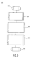
- FIG. 5 is a flow diagram depicting an exemplary method for sensing intensity of a light source in accordance with the present invention.
- Method 500 may utilize one or more systems detailed in FIGS. 1-4 , above.
- Method 500 begins at block 510 where a control system for a light source determines a need to sense the intensity of one or more light emitting diodes (LEDs) or groups of LEDs within the light source. Method 500 allows the control system to determine power requirements for each LED by providing the control system with an intensity value for each LED or group of independently-driven LEDs. Method 500 then advances to block 520.
- LEDs light emitting diodes
- the light source emits a light signal.
- the light source includes at least one light emitting diode (LED) or group of LEDs, each independently-driven LED or group of LEDs emitting a light signal that includes an intensity value within the LED's spectral band, and being driven with a current waveform at a discrete frequency.
- LED light emitting diode
- the light source includes three LEDs or groups of LEDs, each LED or group of LEDs coupled to and receiving a drive signal from an associated control unit (110, 120, and 130), and combining to produce a "white" light output. That is, LED (115) is driven with an AC current at a frequency ⁇ R and emits light in the red spectrum, LED (125) is driven with an AC current at a frequency ⁇ G and emits light in the green spectrum, and LED (135) is driven with an AC current at a frequency ⁇ B and emits light in the blue spectrum.
- a cosine waveform is utilized.
- the resulting light signal is then expressed as: A R ⁇ cos ⁇ R ⁇ t + A G ⁇ cos ⁇ G ⁇ t + A B ⁇ cos ⁇ B ⁇ t where A is the magnitude and ⁇ is the frequency of the associated signal.
- control unit (110) and LED (115) produce the A R cos ⁇ R t component
- control unit (120) and LED (125) produce the A G cos ⁇ G t component
- control unit (130) and LED (135) produce the A B cos ⁇ B t component.
- the red LED (115) is driven at 400 Hz ( ⁇ R )
- the green LED (125) is driven at 500 Hz ( ⁇ G )
- the blue LED (135) is driven at 600 Hz ( ⁇ B ).
- a square wave is utilized as the waveform characteristics include the ability to set the lower portion of the waveform to zero amps.
- the ability to set the lower portion of the waveform to zero is important as it allows for cancellation of undesirable components during production of an output intensity signal.
- the light signal is received by photodetector 150 and transmitted to each lock-in system (170, 180, and 190) as the received light signal.
- the light signal is received by photodetectors 450 and 455, and transmitted to each lock-in system (470, 480, and 490) as the received light signal.
- a portion of the received light signal, received by photodetector 450 is transmitted to one lock-in device (475, 485, and 495) within each lock-in system (470, 480, and 490). Additionally, another portion of the signal, received by photodetector 455, is transmitted to the other lock-in device (477, 487, and 497) within each lock-in system (470, 480, and 490). Method 500 then advances to block 530.
- the control unit transmits a reference signal to an associated lock-in system.
- each control unit (110, 120, and 130) transmits an associated reference signal to an associated lock-in system (170, 180, and 190).
- each reference signal is produced by the associated control unit and transmitted at a discrete frequency.
- control unit 210 receives the clock signal and produces the reference signal based on the clock signal.
- the frequency could be generated internally within each controller thereby negating the need for an external clock.
- a cosine waveform is utilized.
- the resulting reference signal is then expressed as: I ref ⁇ cos ⁇ ref ⁇ t where I ref is the magnitude and ⁇ ref is the frequency of the reference signal.
- control unit 120 the reference signal produced by control unit 120 is expressed as: I ref ⁇ cos ⁇ G ⁇ t
- the reference signal is then transmitted to each lock-in system.
- the reference signal is transmitted to each lock-in system (170, 180, and 190) as the reference signal of FIG.1 , above.
- the reference signal is transmitted to each lock-in system (470, 480, and 490) as the reference signal of FIG. 4 , above.
- Method 500 then advances to block 540.
- each lock-in system (170, 180, and 190) receives the received light signal from photodetector 150 and receives an associated reference signal from an associated control unit (110, 120, and 130).
- signal multiplier 375 of lock-in device 370 receives the received light signal and the associated reference signal.
- signal multiplier 375 produces a product signal by multiplying the received light signal by the associated reference signal.
- the resulting product signal is then expressed as: I ref * A R ⁇ cos ⁇ ref ⁇ t * cos ⁇ R ⁇ t + I ref * A G ⁇ cos ⁇ ref ⁇ t * cos ⁇ G ⁇ t + I ref * A B ⁇ cos ⁇ ref ⁇ t * cos ⁇ B ⁇ t multiplication of the cosine terms results in the product signal expressed as : 1 ⁇ 2I ref * A R ⁇ cos ⁇ ref - ⁇ R ⁇ t + 1 ⁇ 2I ref * A R ⁇ cos ⁇ ref + ⁇ R ⁇ t + 1 ⁇ 2I ref * A G ⁇ cos ⁇ ref - ⁇ G ⁇ t + 1 ⁇ 2I ref * A G ⁇ cos ⁇ ref + ⁇ G ⁇ t + 1 ⁇ 2I ref * A B ⁇ cos ⁇ ref - ⁇ B ⁇ t + 1 ⁇ 2I ref * A B ⁇ cos ⁇ ref + ⁇ B ⁇ t +
- the product signal is then transmitted to filter 377.
- Filter 377 is implemented as a low-pass filter having a cutoff frequency that discards the non-dc terms.
- the cutoff frequency must be less than either ( ⁇ G - ⁇ R ) or ( ⁇ G - ⁇ B ), for example, below 100 Hz when utilizing the above example frequencies.
- the result of filtering the product signal is removal of the non-dc terms and is expressed as: 1 ⁇ 2I ref * A G
- the resulting signal is the intensity value.
- the reference intensity value may be removed, for example, by "dividing" it out. Alternatively, an unaltered intensity value can be returned to the control system.
- each lock-in system receives the received light signal from photodetectors 450 and 455, and receives an associated reference signal from an associated control unit (110, 120, and 130).
- one lock-in device of each lock-in system for example lock-in device 485 of lock-in system 480, receives a portion of the received light signal.
- the second lock-in device of each lock-in system for example lock-in device 487 of lock-in system 480, receives another portion of the received light signal.
- Each lock-in device (485 and 487) produces a component intensity value at the associated intensity signal terminal (Int1/2, Int2/2), as described above.
- the component intensity values are summed to produce a single intensity value for the associated spectrum (e.g. Green).
- the ratio of the two components values provides a measure of any spectral shifts that may have occurred during light source operation.
- Method 500 then advances to block 550, where it returns the intensity values to the control system.
- the control system utilizes the intensity values to determine the amount of power to supply to the LEDs of the light source.
- the control system determines power adjustment requirements by cross indexing each provided LED intensity value with a thermal value (already received).
- each provided LED intensity value and thermal value are cross indexed in a look-up table that includes manufacturer provided data and/or data obtained from LED calibration in the factory.
- the resultant value obtained from the look-up table, for each LED is then utilized by the control system to determine an actual contribution of each LED or independently-driven LED group to the light source. Power supplied to each LED is then adjusted accordingly.
- the control system determines power adjustment requirements by cross indexing each provided summed LED intensity value with a ratio of the component intensity values in a look-up table that includes manufacturer provided data and/or data obtained from LED calibration in the factory.
- the resultant value obtained from the look-up table, for each LED or independently-driven LED group, is then utilized by the control system to determine an actual contribution of each LED to the light source. Power supplied to each LED is then adjusted accordingly.
Description
- The technical field of this disclosure is light production from light emitting diodes (LEDs), particularly, sensing light emitted simultaneously from multiple light sources.
- Illumination sources, such as lamps, currently utilize incandescent and fluorescent means as light production. It is well known that incandescent light sources are inefficient light sources that utilize more power resources than other light sources. Fluorescent light sources have provided a more efficient light production.
- Light emitting diodes (LEDs) produce light in a much more efficient manner than incandescent light sources, but until recently have not been manufactured in a cost efficient manner to utilize in lighting applications. Expectations are for LEDs to produce light more efficiently than fluorescent light sources in the near future. Recently, LED production has made utilizing LEDs in light production applications a viable alternative.
- Producing usable light with LEDs generally requires either manufacturing an LED that produces a specified color, such as utilizing a phosphor layer overlying the LED, or mixing a plurality of colored LEDs to produce a desired colored light output. Unfortunately, once a light source package is produced to achieve the desired colored light output its useful life is reduced to the amount of time until a failure or partial failure of one of its component parts occurs.
- Unfortunately, LED characteristics depend on temperature, drive current, and time. Additionally, LED characteristics vary from LED to LED. Although an LED-based lamp may be set to operate at a given color point and intensity, at the beginning of its life, the actual color and intensity obtained at that setting may not remain constant.
- Mixing a plurality of colored light sources may include a control system that varies individual light source contributions to correct for variation in the LED characteristics That is, as the output of component LEDs varies, the control system can maintain a desired spectral output and intensity by varying individual LED output to compensate for the variations.
- Currently, sensing systems for controlling a specified colored light output include temperature feed-forward or intensity feedback systems containing a single unfiltered photodiode. Another sensing system includes utilizing multiple photodiodes, for example three or more, and corresponding color filters. This system may be referred to as a color filter photodiode control system.
- In one embodiment, this system can be implemented utilizing a time-based approach whereby the LEDs are pulsed on and off in a particular pattern allowing the sensing of the intensity of the independent LED groups. An advantage of the color filter photodiode control system over the temperature feed-forward or intensity feedback systems is that the color filter photodiode control system can sense the average levels of the different spectral outputs of the LEDs, for example red, green, and blue, without having to turn the LEDs on and off in a particular pattern. Additionally, a low pass filter can be used to integrate the signal from each LED group. The accuracy of this method is strongly influenced by the color filters on the photodiodes.
- Unfortunately, as described above, temperature feed-forward or intensity feedback systems require that LEDs be turned on and off briefly to permit sensing of the individual color components, for example red, green and blue. This approach is susceptible to errors resulting from ripple in the driving current, and changes in the drive waveform, such as, for example changes in the rise and fall times of the LED drive current pulses. The color filter photodiode control system, although not requiring the turning on and off of LEDs to sense the individual color components, does require more expensive sensors containing color filters as well as a larger total number of sensors. None of the systems corrects for ambient light.
-
US 6 055 251 A discloses a semiconductor laser control system comprising a control unit for producing a drive signal and a reference signal, a plurality of colored light sources designed to receive the drive signal from an associated control unit and to produce a light signal based on the drive signal, wherein each light source emits a light signal at a discrete frequency and a reference signal at a discrete frequency, a photodetector optically coupled to the plurality of light sources and designed to receive the light signals from the plurality of light sources, and to produce a received light signal, and a lock-in system coupled to the photodectector and each light source, the lock-in system receiving the received light signal from the photodetector and receiving the reference signal from an associated control unit, wherein the lock-in system produces an intensity value of the associated light source based on the received light signal and the reference signal. - It would be desirable, to provide a system that would overcome the above and other disadvantages.
- The present invention is directed to a light source control system for an illumination source. The invention provides for a frequency sensing structure that produces an intensity value input for a control system.
- The invention provides a light source control system according to
claim 1. - The foregoing and other features and advantages of the invention will become further apparent from the following detailed description of the presently preferred embodiment, read in conjunction with the accompanying drawings. The detailed description and drawings are merely illustrative of the invention rather than limiting, the scope of the invention being defined by the appended claims and equivalents thereof.
-
FIG. 1 is a schematic diagram illustrating a sensing device according to an embodiment of the present invention; -
FIG. 2 is a schematic diagram illustrating a portion of the sensing device inFIG. 1 according to an embodiment of the present invention; -
FIG. 3 is a schematic diagram illustrating another portion of the sensing device inFIG. 1 according to an embodiment of the present invention; -
FIG. 4 is a schematic diagram illustrating a sensing device according to another embodiment of the present invention; and -
FIG. 5 is a flow diagram depicting an exemplary method in accordance with the present invention. - Throughout the specification, and in the claims, the term "connected" means a direct physical or optical connection between the things that are connected, without any intermediate devices. The term "coupled" means either a direct physical or optical connection between the things that are connected or an indirect connection through one or more passive or active intermediary devices. The term "circuit" means either a single component or a multiplicity of components, either active or passive, that are coupled together to perform a desired function.
-
FIG. 1 is a schematic diagram illustrating asensing device 100 according to an embodiment of the present invention.Device structure 100 includes control units (110, 120, and 130), light emitting diodes (115, 125 and 135), aphotodetector 150, and lock-in systems (170, 180, and 190). In one embodiment, implementation of the present invention allows any number of light emitting diodes (LEDs) to be utilized, so long as there is a corresponding control unit and lock-in system for each LED. In another embodiment, each LED represents a block of independently-driven LEDs with a substantially similar spectral light output. For example,LED 115 may consist of several LEDs, all emitting a red light output. Similarly,LED 125 may include all green light emitting LEDs, andLED 135 may include all blue light emitting LEDs. - In one example, the present invention is implemented as a single LED or a single color group of LEDs, a single control unit, and a single lock-in unit in addition to the photodetector. In another example and referring to
FIG. 1 ,sensing device 100 is implemented as a plurality of LEDs or multi-color LED groups, each independently-driven LED or LED group having an associated control unit and an associated lock-in system. In this example, emitted spectra of the LEDs form a multi-source light signal. For example, a red, a green, and a blue LED or groups of LEDs are utilized to produce a "white" multi-source light signal. - Each control unit (110, 120, and 130), detailed in
FIG. 2 below, includes an associated output drive signal terminal (Drv1, Drv2, and Drv3) and an associated output reference terminal (Ref1, Ref2, and Ref3). Each output drive signal terminal (Drv1, Drv2, and Drv3) is coupled to an associated light emitting diode (115, 125 and 135).
In an example, output drive signal terminal (Drv1) is coupled to light emitting diodes (115), output drive signal terminal (Drv2) is coupled to light emitting diode (125), and output drive signal terminal (Drv3) is coupled to light emitting diode (135).
Light emitting diodes (115, 125 and 135) are optoelectronic devices that produce light when power is supplied causing them to forward bias. The light produced may be within the blue, green, red, amber or other portion of the spectrum, depending on the material utilized in manufacturing the LED. In an example, LEDs (115, 125 and 135) are implemented as LXHL-BM01, LXHL-BB01 and LXHL-BD01 available from Lumileds corporation of San Jose, CA. In another example, LEDs (115, 125 and 135) are implemented as NSPB300A, NSPG300A and NSPR800AS from Nichia corporation of Mountville, PA. - Each control unit produces a drive signal and a reference signal, as detailed in
FIG. 2 below. Power, in the form of the drive signal, is transmitted to the associated light emitting diode (LED) or LED group and the reference signal is transmitted to the associated lock-in unit. The LED receives the drive signal and produces a light signal based on the drive signal. The drive signal is generated at a discrete frequency.
The reference signal is transmitted to the associated lock-in system and includes the same discrete frequency. Multiple control units and associated LEDs produce a light signal including several intensity values representing the intensity of light emitted by each LED or LED group. - It is important to differentiate between the discrete frequency driving the light signal emitting from each LED or LED group and the very high frequency that the LED or LED group emit as light. Typically, as described below, the frequency of the drive signals ranges from about 400 Hz to about 1.2 kHz while the frequency of the light emitted from the LEDs or LED groups is in the order of 1014 Hz.
- Photodetector 150 is an optoelectronic device that responds to light signals and produces a received light signal. In one embodiment,
photodetector 150 is implemented as a photodiode, such as, for example PS 1-2CH from Pacific Silicon Sensor, Inc of Westlake Village, CA.Photodetector 150 includes an output signal terminal (Rec) for supplying the received light signal. - In one embodiment,
photodetector 150 responds to a single source light signal and produces a received light signal, at the output signal terminal (Rec), which corresponds to the intensity of light produced by that single light source. In another embodiment and described inFIG. 5 below,photodetector 150 responds to the multi-source light signal and produces a received light signal, at the output signal terminal (Rec). The received light signal includes components at multiple frequencies, each component corresponding to the intensity of one light source in the multi-source light signal. - Each lock-in system (170, 180, and 190) includes a lock-in device, detailed in
FIG. 3 below. Each lock-in system (170, 180, and 190) further includes an input signal terminal (Rec) and an associated input reference terminal (Ref1, Ref2, and Ref3). Each input signal terminal (Rec) of each associated lock-in system (170, 180, and 190) is coupled to the output signal terminal (Rec) ofphotodetector 150. Each input reference terminal (Ref1, Ref2, and Ref3) of each associated lock-in system (170, 180, and 190) is coupled to the output reference terminal (Ref1, Ref2, and Ref3) of each associated control unit (110, 120, and 130). - In an example, output reference terminal (Ref1) of
control unit 110 is coupled to input reference terminal (Ref1) of lock-insystem 170, output reference terminal (Ref2) ofcontrol unit 120 is coupled to input reference terminal (Ref1) of lock-insystem 180, and output reference terminal (Ref3) ofcontrol unit 130 is coupled to input reference terminal (Ref3) of lock-insystem 190. - Each lock-in system (170, 180, and 190) further includes an associated output intensity signal terminal (Int1, Int2, and Int3), detailed in
FIG. 3 below. Each lock-in system receives an input signal, at the input signal terminal (Rec), fromphotodetector 150 and a reference signal, at the input reference terminal (Ref1, Ref2, and Ref3), from an associated control unit (110, 120, and 130). Each lock-in system produces an output intensity signal, at the associated output intensity signal terminal (Int1, Int2, and Int3), based on the received input signal and reference signal. - In a further embodiment,
sensing device 100 includes a high-pass filter coupled between the output reference terminal (Ref1, Ref2, and Ref3) of each control unit (110, 120, and 130) and the input reference terminal (Ref1, Ref2, and Ref3) of the associated lock-in system (170, 180, and 190). In one embodiment, coupling a high-pass filter between the control unit and the lock-in system reduces spurious dc components from affecting the reference signal. -
FIG. 2 is a schematic diagram illustrating acontrol unit 210 according to an embodiment of the present invention.Control unit 210 includes afrequency shifter 215, apower distributor 217, an input clock signal terminal (Clk), an input power signal terminal (Pwr), an output reference signal terminal (Ref), and an output drive signal terminal.Control unit 210 receives a clock signal and a power signal, produces a reference signal based on the clock signal, and produces a drive signal based on the reference signal and the power signal. -
Frequency shifter 215 includes an input clock signal terminal (Clk) and an output reference signal terminal (Ref).Frequency shifter 215 receives the clock signal and produces the reference signal based on the clock signal. In one embodiment,frequency shifter 215 receives the clock signal and "divides down" the clock signal to produce the reference signal. The reference signal frequency utilized is produced at a frequency so as not to cause noticeable "flicker" to the human eye. In an example, a reference signal is produced in the 100 Hz - 2.4 kHz range. - In another embodiment,
frequency shifter 215 includes an internal clock that generates the clock signal internally thereby eliminating the need for the clock terminal (Clk): - Additionally and referring to
FIG.1 , the use of multiple control units (110, 120, and 130) requires several discrete frequencies. The frequencies utilized are produced so that frequency overlap will not occur. In one embodiment, the frequencies utilized are produced with a 100 Hz gap between discrete frequencies. In an example,control unit 110 produces a reference frequency at 400 Hz,control unit 120 produces a reference frequency at 500 Hz, andcontrol unit 130 produces a reference frequency at 600 Hz. -
Power distributor 217 includes an input power terminal (Pwr), an input reference signal terminal (Ref), and an output drive signal terminal (Drv). The input reference terminal (Ref) ofpower distributor 217 is coupled to the output reference terminal (Ref) offrequency shifter 215.Power distributor 217 receives the power signal and the reference signal and produces the drive signal based on the power signal and the reference signal. - In one embodiment, the power signal is implemented as a voltage source signal. In another embodiment, the power signal is implemented as a current source signal. In an example,
power distributor 217 produces a drive signal including a current signal modulated at a discrete frequency associated with the reference signal. - The power signal may be produced in the form of one of several different waveforms, such as, for example, a sine wave, a cosine wave, a square wave, or any other waveform that would allow the production of the light signal.
-
FIG. 3 is a schematic diagram illustrating a lock-indevice 370 according to an embodiment of the present invention. Lock-indevice 370 includes asignal multiplier 375, afilter 377, an input signal terminal (Rec), an input reference terminal (Ref), and an output intensity terminal (Int). Lock-indevice 370 receives an input signal and a reference signal, and produces an intensity signal based on the input signal and the reference signal. -
Signal multiplier 375 includes an input signal terminal (Rec), an input reference terminal (Ref), and an output product terminal (Prd).Signal multiplier 375 receives the input signal and the reference signal, and produces a product signal based on the input signal and the reference signal.Signal multiplier 375 produces the product signal by multiplying the input signal by the reference signal, detailed inFIG. 5 below.Signal multiplier 375 can be implemented as a signal multiplier chip, such as, for example the MLT04 produced by Analog Devices of Norwood, MA. -
Filter 377 includes an input product terminal (Prd) and an output intensity terminal (Int). The input product terminal (Prd) offilter 377 is coupled to the output product terminal (Prd) ofsignal multiplier 375.Filter 377 receives the product signal and filters the received product signal to remove non-dc portions of the signal. In one embodiment,filter 377 is implemented as a low-pass filter. -
FIG. 4 is a schematic diagram illustrating asensing device 400 according to another embodiment of the present invention.Device structure 400 includes control units (110, 120, and 130), light emitting diodes (115, 125 and 135),photodetectors FIG.1 are numbered identically and function identically. In one embodiment, implementation of the present invention allows any number of light emitting diodes (LEDs) to be utilized, so long as there is a corresponding control unit and lock-in system for each independently driven LED or group of LEDs. -
Photodetectors photodetectors photodetector 450 includes an output signal terminal (Rec1) for supplying a portion of the received light signal, andphotodetector 455 includes an output signal terminal (Rec2) for supplying another portion of the received light signal. - In another embodiment,
photodetectors photodetector 450 represents a first junction of the multi-junction photodiode, andphotodetector 455 represents a second junction of the multi-junction photodiode. One junction is more sensitive to red wavelengths, and the other is more sensitive to blue wavelengths. Comparison of the measurements of the two junctions provides a measure of spectral shift. - In an example,
photodetector 450 responds more strongly thanphotodetector 455 to light signals within the spectrum defined as greater than about 600nm. In this example,photodetector 455 responds most strongly thanphotodetector 450 to light signals within the spectrum defined as less than about 600nm. -
Photodetectors - In another embodiment, each received light signal includes components at single or multiple frequencies. In this embodiment, each component corresponds to the intensity of one light source in the multi-source light signal.
- Each lock-in system (470, 480, and 490) includes multiple lock-in devices (475, 477, 485, 487, 495, and 497), each lock-in device functions as described in
FIG. 3 above. In one embodiment, the number of lock-in devices within each lock-in system is equal to the number of photodetectors. In an example, lock-in devices (475, 485, and 495) are coupled tophotodetector 450 via input signal terminal (Rec1), and lock-in devices (477, 487, and 497) are coupled tophotodetector 455 via input signal terminal (Rec2). - Each lock-in system (470, 480, and 490) further includes associated input reference terminals (Ref1, Ref2, and Ref3). Input reference terminals (Ref1, Ref2, and Ref3) of each associated lock-in system (470, 480, and 490) are coupled to the output reference terminal (Ref1, Ref2, and Ref3) of each associated control unit (110, 120, and 130). In an example, output reference terminal (Ref1) of
control unit 110 is coupled to each input reference terminal (Ref1) of lock-in devices (475 and 477) within lock-insystem 470. Output reference terminal (Ref2) ofcontrol unit 120 is coupled to input reference terminal (Ref1) of lock-in devices (485 and 487) within lock-insystem 480. Output reference terminal (Ref3) ofcontrol unit 130 is coupled to input reference terminal (Ref3) of lock-in devices (495 and 497) within lock-insystem 490. - Each lock-in device (475, 477, 485, 487, 495, and 497) further includes multiple output intensity signal terminals (Int1/1, Int2/1, Int1/2, Int2/2, Int1/3, and Int2/3). In one embodiment, the number of output intensity signal terminals within each lock-in system is equal to the number of lock-in devices, and therefore is equal to the number of photodetectors.
- Each lock-in device receives a portion of the received light signal from an associated photodetector, and receives a reference signal from an associated control unit. Each lock-in system produces an output intensity signal, at the associated output intensity signal terminal (Int1/1, Int2/1, Int1/2, Int2/2, Int1/3, and Int2/3), based on the received input signal and reference signal.
- In a further embodiment,
sensing device 400 includes a high-pass filter coupled between the output reference terminal (Ref1, Ref2, and Ref3) of each control unit (110, 120, and 130) and the input reference terminal (Ref1, Ref2, and Ref3) of the associated lock-in system (470, 480, and 490). In one embodiment, coupling a high-pass filter between the control unit and the lock-in system reduces spurious dc components from affecting the reference signal. -
FIG. 5 is a flow diagram depicting an exemplary method for sensing intensity of a light source in accordance with the present invention.Method 500 may utilize one or more systems detailed inFIGS. 1-4 , above. -
Method 500 begins atblock 510 where a control system for a light source determines a need to sense the intensity of one or more light emitting diodes (LEDs) or groups of LEDs within the light source.Method 500 allows the control system to determine power requirements for each LED by providing the control system with an intensity value for each LED or group of independently-driven LEDs.Method 500 then advances to block 520. - At
block 520, the light source emits a light signal. Referring toFIGS. 1 and2 , the light source includes at least one light emitting diode (LED) or group of LEDs, each independently-driven LED or group of LEDs emitting a light signal that includes an intensity value within the LED's spectral band, and being driven with a current waveform at a discrete frequency. - In an example, the light source includes three LEDs or groups of LEDs, each LED or group of LEDs coupled to and receiving a drive signal from an associated control unit (110, 120, and 130), and combining to produce a "white" light output. That is, LED (115) is driven with an AC current at a frequency ωR and emits light in the red spectrum, LED (125) is driven with an AC current at a frequency ωG and emits light in the green spectrum, and LED (135) is driven with an AC current at a frequency ωB and emits light in the blue spectrum. For illustrative purposes, a cosine waveform is utilized. The resulting light signal is then expressed as:

where A is the magnitude and ω is the frequency of the associated signal. - In this example control unit (110) and LED (115) produce the AR cosωRt component, control unit (120) and LED (125) produce the AG cosωGt component, and control unit (130) and LED (135) produce the AB cosωBt component. In this example and referring to
FIG. 1 , the red LED (115) is driven at 400 Hz (ωR), the green LED (125) is driven at 500 Hz (ωG), and the blue LED (135) is driven at 600 Hz (ωB). - In one embodiment, a square wave is utilized as the waveform characteristics include the ability to set the lower portion of the waveform to zero amps. The ability to set the lower portion of the waveform to zero is important as it allows for cancellation of undesirable components during production of an output intensity signal.
- In one embodiment and referring to
FIGS. 1 and3 above, the light signal is received byphotodetector 150 and transmitted to each lock-in system (170, 180, and 190) as the received light signal. In another embodiment and referring toFIGS. 3 and4 above, the light signal is received byphotodetectors - In this embodiment, a portion of the received light signal, received by
photodetector 450, is transmitted to one lock-in device (475, 485, and 495) within each lock-in system (470, 480, and 490). Additionally, another portion of the signal, received byphotodetector 455, is transmitted to the other lock-in device (477, 487, and 497) within each lock-in system (470, 480, and 490).Method 500 then advances to block 530. - At
block 530, the control unit transmits a reference signal to an associated lock-in system. In one embodiment and referring toFIG.1 , each control unit (110, 120, and 130) transmits an associated reference signal to an associated lock-in system (170, 180, and 190). In this embodiment, each reference signal is produced by the associated control unit and transmitted at a discrete frequency. - In an example and referring to
FIGS. 1 and2 ,control unit 210 receives the clock signal and produces the reference signal based on the clock signal. Alternatively and detailed inFIG. 2 above, the frequency could be generated internally within each controller thereby negating the need for an external clock. Additionally, for illustrative purposes a cosine waveform is utilized. The resulting reference signal is then expressed as:
where Iref is the magnitude and ωref is the frequency of the reference signal. - In this example, the reference signal produced by
control unit 120 is expressed as:
- The reference signal is then transmitted to each lock-in system. In one embodiment, the reference signal is transmitted to each lock-in system (170, 180, and 190) as the reference signal of
FIG.1 , above. In another embodiment, the reference signal is transmitted to each lock-in system (470, 480, and 490) as the reference signal ofFIG. 4 , above.Method 500 then advances to block 540. - At
block 540, the lock-in system produces an intensity value based on the received light signal and the associated reference signal. In one embodiment and referring toFIG. 1 , each lock-in system (170, 180, and 190) receives the received light signal fromphotodetector 150 and receives an associated reference signal from an associated control unit (110, 120, and 130). - In an example and referring to
FIGS. 1 and3 ,signal multiplier 375 of lock-indevice 370 receives the received light signal and the associated reference signal. In this example,signal multiplier 375 produces a product signal by multiplying the received light signal by the associated reference signal. The resulting product signal is then expressed as:

- In this example and described above, lock-in
device 370 represents the lock-in device within lock-insystem 180 ofFIG.1 , above. Therefore, the resulting reference signal is produced bycontrol unit 120 and expressed as:
substitution results in the product signal expressed as:
- In this example, the product signal is then transmitted to filter 377.
Filter 377 is implemented as a low-pass filter having a cutoff frequency that discards the non-dc terms. The cutoff frequency must be less than either (ωG - ωR) or (ωG - ωB), for example, below 100 Hz when utilizing the above example frequencies. The result of filtering the product signal is removal of the non-dc terms and is expressed as:
- In this example and referring to
FIGS. 1 and3 , the resulting signal is the intensity value. The reference intensity value may be removed, for example, by "dividing" it out. Alternatively, an unaltered intensity value can be returned to the control system. - In another embodiment and referring to
FIG. 4 , each lock-in system (470, 480, and 490) receives the received light signal fromphotodetectors device 485 of lock-insystem 480, receives a portion of the received light signal. The second lock-in device of each lock-in system, for example lock-indevice 487 of lock-insystem 480, receives another portion of the received light signal. Each lock-in device (485 and 487) produces a component intensity value at the associated intensity signal terminal (Int1/2, Int2/2), as described above. In an example, the component intensity values are summed to produce a single intensity value for the associated spectrum (e.g. Green). In an example, the ratio of the two components values provides a measure of any spectral shifts that may have occurred during light source operation.Method 500 then advances to block 550, where it returns the intensity values to the control system. - The control system utilizes the intensity values to determine the amount of power to supply to the LEDs of the light source. In one embodiment and referring to
FIG. 1 , the control system determines power adjustment requirements by cross indexing each provided LED intensity value with a thermal value (already received). In an example, each provided LED intensity value and thermal value are cross indexed in a look-up table that includes manufacturer provided data and/or data obtained from LED calibration in the factory. The resultant value obtained from the look-up table, for each LED, is then utilized by the control system to determine an actual contribution of each LED or independently-driven LED group to the light source. Power supplied to each LED is then adjusted accordingly. - In another embodiment and referring to
FIG. 4 , the control system determines power adjustment requirements by cross indexing each provided summed LED intensity value with a ratio of the component intensity values in a look-up table that includes manufacturer provided data and/or data obtained from LED calibration in the factory. The resultant value obtained from the look-up table, for each LED or independently-driven LED group, is then utilized by the control system to determine an actual contribution of each LED to the light source. Power supplied to each LED is then adjusted accordingly. - The above-described apparatus and method for sensing light emitted simultaneously from multiple light sources are example methods and implementations. These methods and implementations illustrate one possible approach for sensing light emitted simultaneously from multiple light sources. The actual implementation may vary from the method discussed. Moreover, various other improvements and modifications to this invention may occur to those skilled in the art, and those improvements and modifications will fall within the scope of this invention as set forth in the claims below.
- The present invention may be embodied in other specific forms without departing from its essential characteristics. The described embodiments are to be considered in all respects only as illustrative and not restrictive.
Claims (11)
- A light source control system for an illumination source, comprising:- a plurality of control units (110, 120, 130) for producing a drive signal (Drv1, Drv2, Drv3) and a reference signal (Ref1, Ref2, Ref3) at the same discrete frequency as the drive signal;- a plurality of colored light sources (115, 125, 135) designed to receive the drive signal from an associated control unit (110, 120, 130) and to produce a light signal based on the drive signal;- each colored light source emitting a light signal at a drive signal frequency, wherein the light signals of each of the plurality of colored light sources are mixed to produce a desired colored light output for illumination,- a photodetector (150; 450, 455) optically coupled to the plurality of light sources, the photodetector designed to receive the light signals from the plurality of light sources, and to produce a received light signal; and- a plurality of lock-in systems (170, 180, 190; 470, 480, 490) coupled to the photodetector (150; 450, 455) and each light source, each lock-in system receiving the received light signal from the photodector and receiving the reference signal from an associated control unit (110, 120, 130), wherein each lock-in system produces an intensity value of the associated light source based on the received light signal and the reference signal, and wherein each lock-in system comprises a signal multiplier (375), and a filter (377) coupled to the signal multiplier, and wherein the intensity value is the product of the received light signal and the reference signal processed through the signal multiplier, and filtered by the filter to remove non-dc portions.
- The systemof claim 1, wherein the plurality of colored light sources each comprise one or more colored LEDs.
- The system of claim 1 wherein the control unit (210) is designed to receive a clock signal and a power signal, produce the reference signal at the discrete frequency based on the clock signal, and produce the drive signal based on the reference signal and the power signal.
- The system of claim 1 wherein the photodetector comprises a single-junction photodiode.
- The system of claim 1 wherein the intensity value is the intensity of the light signal at the associated discrete frequency.
- The system of claim 1 wherein the photodetector comprises a multi-junction photodiode.
- The system of claim 6 wherein each junction of the multi-junction photodiode receives a portion of the light signal, the portion of the light signal received based on an associated spectra of the light signal.
- The system of claim 7 wherein the at least one lock-in system (470, 480, 490) comprises a plurality of lock-in devices (475, 477, 485, 487, 495, 497), each lock-in device coupled to the photodetector (450, 455) to receive a portion of the light signal.
- The system of claim 8 wherein a partial intensity value is produced in each lock-in device (475, 477, 485, 487, 495, 497) from the product of the portion of the light signal received by the lock-in device and the reference signal processed through the signal multiplier (375), and filtered by the filter (377) to remove non-dc portions.
- The system of claim 9 wherein the intensity value is the sum of the partial intensity values.
- The system of claim 1 wherein the filter is a low-pass filter.
Applications Claiming Priority (3)
| Application Number | Priority Date | Filing Date | Title |
|---|---|---|---|
| US43524302P | 2002-12-20 | 2002-12-20 | |
| US435243P | 2002-12-20 | ||
| PCT/IB2003/005983 WO2004057923A1 (en) | 2002-12-20 | 2003-12-12 | Sensing light emitted from multiple light sources |
Publications (2)
| Publication Number | Publication Date |
|---|---|
| EP1579732A1 EP1579732A1 (en) | 2005-09-28 |
| EP1579732B1 true EP1579732B1 (en) | 2014-06-18 |
Family
ID=32682197
Family Applications (1)
| Application Number | Title | Priority Date | Filing Date |
|---|---|---|---|
| EP03777092.2A Expired - Lifetime EP1579732B1 (en) | 2002-12-20 | 2003-12-12 | Sensing light emitted from multiple light sources |
Country Status (7)
| Country | Link |
|---|---|
| US (1) | US7432668B2 (en) |
| EP (1) | EP1579732B1 (en) |
| JP (1) | JP4818610B2 (en) |
| CN (1) | CN100482011C (en) |
| AU (1) | AU2003286348A1 (en) |
| TW (1) | TWI343658B (en) |
| WO (1) | WO2004057923A1 (en) |
Families Citing this family (67)
| Publication number | Priority date | Publication date | Assignee | Title |
|---|---|---|---|---|
| US7026769B2 (en) | 2003-12-18 | 2006-04-11 | Joon Chok Lee | Luminary control system adapted for reproducing the color of a known light source |
| US20050259424A1 (en) | 2004-05-18 | 2005-11-24 | Zampini Thomas L Ii | Collimating and controlling light produced by light emitting diodes |
| WO2006006537A1 (en) * | 2004-07-12 | 2006-01-19 | Sony Corporation | Drive device for back light unit and drive method therefor |
| WO2007004108A1 (en) * | 2005-06-30 | 2007-01-11 | Koninklijke Philips Electronics N.V. | Method and system for controlling the output of a luminaire |
| US7317288B2 (en) * | 2005-09-02 | 2008-01-08 | Au Optronics Corporation | Controlling method and system for LED-based backlighting source |
| EP1961270A1 (en) * | 2005-12-09 | 2008-08-27 | Koninklijke Philips Electronics N.V. | Device for determining characteristics of a lighting unit |
| CA2649915A1 (en) * | 2006-04-20 | 2007-11-01 | University Of Utah Research Foundation | Polymeric compositions and methods of making and using thereof |
| US8747870B2 (en) | 2006-04-20 | 2014-06-10 | University Of Utah Research Foundation | Polymeric compositions and methods of making and using thereof |
| CA2648723A1 (en) * | 2006-04-21 | 2007-11-01 | Tir Technology Lp | Method and apparatus for light intensity control |
| US7766511B2 (en) | 2006-04-24 | 2010-08-03 | Integrated Illumination Systems | LED light fixture |
| US7729941B2 (en) | 2006-11-17 | 2010-06-01 | Integrated Illumination Systems, Inc. | Apparatus and method of using lighting systems to enhance brand recognition |
| WO2008083695A1 (en) * | 2006-12-20 | 2008-07-17 | Patent-Treuhand-Gesellschaft für elektrische Glühlampen mbH | Device and method for measuring the intensity of the light of a first group of light sources of a lighting unit |
| US8013538B2 (en) | 2007-01-26 | 2011-09-06 | Integrated Illumination Systems, Inc. | TRI-light |
| CN101940062B (en) | 2007-08-07 | 2014-03-12 | 皇家飞利浦电子股份有限公司 | Method and apparatus for discriminating modulated light in mixed light system |
| DE102007039388A1 (en) | 2007-08-21 | 2009-02-26 | Zumtobel Lighting Gmbh | Lighting arrangement with light source and sensor for detecting the light indicated by the light source |
| DE102007045259A1 (en) | 2007-09-21 | 2009-04-02 | Continental Automotive Gmbh | Method and device for detecting the light output emitted by an LED light source |
| US8742686B2 (en) | 2007-09-24 | 2014-06-03 | Integrated Illumination Systems, Inc. | Systems and methods for providing an OEM level networked lighting system |
| WO2009040705A2 (en) * | 2007-09-28 | 2009-04-02 | Koninklijke Philips Electronics N.V. | Method and apparatus for light intensity control with drive current modulation |
| EP2091301B1 (en) | 2008-02-07 | 2013-04-10 | Tridonic Jennersdorf GmbH | Light measurement system comprising LEDs |
| US8255487B2 (en) | 2008-05-16 | 2012-08-28 | Integrated Illumination Systems, Inc. | Systems and methods for communicating in a lighting network |
| US20100007588A1 (en) * | 2008-07-09 | 2010-01-14 | Adaptive Micro Systems Llc | System and method for led degradation and temperature compensation |
| EP2374330A2 (en) * | 2008-12-05 | 2011-10-12 | Koninklijke Philips Electronics N.V. | Method and system of controlling illumination characteristics of a plurality of lighting segments |
| US8339058B2 (en) * | 2008-12-12 | 2012-12-25 | Microchip Technology Incorporated | Three-color RGB LED color mixing and control by variable frequency modulation |
| US8339068B2 (en) * | 2008-12-12 | 2012-12-25 | Microchip Technology Incorporated | LED brightness control by variable frequency modulation |
| US8585245B2 (en) | 2009-04-23 | 2013-11-19 | Integrated Illumination Systems, Inc. | Systems and methods for sealing a lighting fixture |
| DE102009022244A1 (en) | 2009-05-22 | 2011-01-27 | Ledon Lighting Gmbh | Lighting arrangement with at least one light source |
| US10264637B2 (en) | 2009-09-24 | 2019-04-16 | Cree, Inc. | Solid state lighting apparatus with compensation bypass circuits and methods of operation thereof |
| US9713211B2 (en) | 2009-09-24 | 2017-07-18 | Cree, Inc. | Solid state lighting apparatus with controllable bypass circuits and methods of operation thereof |
| US8901845B2 (en) | 2009-09-24 | 2014-12-02 | Cree, Inc. | Temperature responsive control for lighting apparatus including light emitting devices providing different chromaticities and related methods |
| US8476836B2 (en) | 2010-05-07 | 2013-07-02 | Cree, Inc. | AC driven solid state lighting apparatus with LED string including switched segments |
| US8390205B2 (en) | 2010-09-01 | 2013-03-05 | Osram Sylvania Inc. | LED control using modulation frequency detection techniques |
| US10098197B2 (en) | 2011-06-03 | 2018-10-09 | Cree, Inc. | Lighting devices with individually compensating multi-color clusters |
| US10178723B2 (en) | 2011-06-03 | 2019-01-08 | Cree, Inc. | Systems and methods for controlling solid state lighting devices and lighting apparatus incorporating such systems and/or methods |
| US9066381B2 (en) | 2011-03-16 | 2015-06-23 | Integrated Illumination Systems, Inc. | System and method for low level dimming |
| US8950892B2 (en) | 2011-03-17 | 2015-02-10 | Cree, Inc. | Methods for combining light emitting devices in a white light emitting apparatus that mimics incandescent dimming characteristics and solid state lighting apparatus for general illumination that mimic incandescent dimming characteristics |
| US9839083B2 (en) | 2011-06-03 | 2017-12-05 | Cree, Inc. | Solid state lighting apparatus and circuits including LED segments configured for targeted spectral power distribution and methods of operating the same |
| US8710770B2 (en) | 2011-07-26 | 2014-04-29 | Hunter Industries, Inc. | Systems and methods for providing power and data to lighting devices |
| US20150237700A1 (en) | 2011-07-26 | 2015-08-20 | Hunter Industries, Inc. | Systems and methods to control color and brightness of lighting devices |
| US10874003B2 (en) | 2011-07-26 | 2020-12-22 | Hunter Industries, Inc. | Systems and methods for providing power and data to devices |
| US11917740B2 (en) | 2011-07-26 | 2024-02-27 | Hunter Industries, Inc. | Systems and methods for providing power and data to devices |
| US9609720B2 (en) | 2011-07-26 | 2017-03-28 | Hunter Industries, Inc. | Systems and methods for providing power and data to lighting devices |
| US9521725B2 (en) | 2011-07-26 | 2016-12-13 | Hunter Industries, Inc. | Systems and methods for providing power and data to lighting devices |
| US8742671B2 (en) | 2011-07-28 | 2014-06-03 | Cree, Inc. | Solid state lighting apparatus and methods using integrated driver circuitry |
| US10043960B2 (en) | 2011-11-15 | 2018-08-07 | Cree, Inc. | Light emitting diode (LED) packages and related methods |
| US8729815B2 (en) | 2012-03-12 | 2014-05-20 | Osram Sylvania Inc. | Current control system |
| US8894437B2 (en) | 2012-07-19 | 2014-11-25 | Integrated Illumination Systems, Inc. | Systems and methods for connector enabling vertical removal |
| US9513113B2 (en) | 2012-10-29 | 2016-12-06 | 7D Surgical, Inc. | Integrated illumination and optical surface topology detection system and methods of use thereof |
| US9379578B2 (en) | 2012-11-19 | 2016-06-28 | Integrated Illumination Systems, Inc. | Systems and methods for multi-state power management |
| US9420665B2 (en) | 2012-12-28 | 2016-08-16 | Integration Illumination Systems, Inc. | Systems and methods for continuous adjustment of reference signal to control chip |
| US9485814B2 (en) | 2013-01-04 | 2016-11-01 | Integrated Illumination Systems, Inc. | Systems and methods for a hysteresis based driver using a LED as a voltage reference |
| US10231300B2 (en) | 2013-01-15 | 2019-03-12 | Cree, Inc. | Systems and methods for controlling solid state lighting during dimming and lighting apparatus incorporating such systems and/or methods |
| US10264638B2 (en) | 2013-01-15 | 2019-04-16 | Cree, Inc. | Circuits and methods for controlling solid state lighting |
| US20150029693A1 (en) * | 2013-07-23 | 2015-01-29 | Delphi Technologies, Inc. | Vehicle instrument panel with light source diagnostics |
| US9578724B1 (en) | 2013-08-20 | 2017-02-21 | Ketra, Inc. | Illumination device and method for avoiding flicker |
| USRE48955E1 (en) | 2013-08-20 | 2022-03-01 | Lutron Technology Company Llc | Interference-resistant compensation for illumination devices having multiple emitter modules |
| USRE48956E1 (en) | 2013-08-20 | 2022-03-01 | Lutron Technology Company Llc | Interference-resistant compensation for illumination devices using multiple series of measurement intervals |
| US9557214B2 (en) | 2014-06-25 | 2017-01-31 | Ketra, Inc. | Illumination device and method for calibrating an illumination device over changes in temperature, drive current, and time |
| US9736903B2 (en) * | 2014-06-25 | 2017-08-15 | Ketra, Inc. | Illumination device and method for calibrating and controlling an illumination device comprising a phosphor converted LED |
| US9510416B2 (en) | 2014-08-28 | 2016-11-29 | Ketra, Inc. | LED illumination device and method for accurately controlling the intensity and color point of the illumination device over time |
| US9392660B2 (en) | 2014-08-28 | 2016-07-12 | Ketra, Inc. | LED illumination device and calibration method for accurately characterizing the emission LEDs and photodetector(s) included within the LED illumination device |
| US10918030B2 (en) | 2015-05-26 | 2021-02-16 | Hunter Industries, Inc. | Decoder systems and methods for irrigation control |
| US10228711B2 (en) | 2015-05-26 | 2019-03-12 | Hunter Industries, Inc. | Decoder systems and methods for irrigation control |
| US10060599B2 (en) | 2015-05-29 | 2018-08-28 | Integrated Illumination Systems, Inc. | Systems, methods and apparatus for programmable light fixtures |
| US10030844B2 (en) | 2015-05-29 | 2018-07-24 | Integrated Illumination Systems, Inc. | Systems, methods and apparatus for illumination using asymmetrical optics |
| US11272599B1 (en) | 2018-06-22 | 2022-03-08 | Lutron Technology Company Llc | Calibration procedure for a light-emitting diode light source |
| DE102018212529A1 (en) * | 2018-07-27 | 2020-01-30 | Robert Bosch Gmbh | Method and control device for regulating an emitted light output of a light source of an optical sensor system |
| US10801714B1 (en) | 2019-10-03 | 2020-10-13 | CarJamz, Inc. | Lighting device |
Family Cites Families (13)
| Publication number | Priority date | Publication date | Assignee | Title |
|---|---|---|---|---|
| US3328686A (en) * | 1964-08-31 | 1967-06-27 | Weston Instruments Inc | D.c. analog spectrum analyzer |
| US3439283A (en) * | 1966-02-04 | 1969-04-15 | Gen Electric | Frequency shift keyed discriminating circuits |
| US3439269A (en) * | 1966-12-30 | 1969-04-15 | Weston Instruments Inc | Multichannel analog analyzer |
| US3876946A (en) * | 1973-10-31 | 1975-04-08 | Singer Co | Radio frequency digital fourier analyzer |
| CA1279414C (en) * | 1987-06-26 | 1991-01-22 | Makoto Nishio | Apparatus for discriminating an optical signal from others and an apparatus for tuning an optical wavelength filter used in the same |
| US5192856A (en) * | 1990-11-19 | 1993-03-09 | An Con Genetics, Inc. | Auto focusing bar code reader |
| FR2671187A1 (en) * | 1990-12-28 | 1992-07-03 | Cga Hbs | NON-DESTRUCTIVE CONTROL DEVICE WITH CURRENT FOUCAULT. |
| CA2132043C (en) * | 1993-09-17 | 1999-03-23 | Toshihiko Ouchi | Method and apparatus for frequency modulating a semiconductor laser, and an optical communication system using the same |
| US7064498B2 (en) * | 1997-08-26 | 2006-06-20 | Color Kinetics Incorporated | Light-emitting diode based products |
| US6965205B2 (en) * | 1997-08-26 | 2005-11-15 | Color Kinetics Incorporated | Light emitting diode based products |
| JP3696839B2 (en) * | 2001-03-14 | 2005-09-21 | 松下電器産業株式会社 | Lighting device |
| US6753661B2 (en) * | 2002-06-17 | 2004-06-22 | Koninklijke Philips Electronics N.V. | LED-based white-light backlighting for electronic displays |
| US6998594B2 (en) * | 2002-06-25 | 2006-02-14 | Koninklijke Philips Electronics N.V. | Method for maintaining light characteristics from a multi-chip LED package |
-
2003
- 2003-12-12 US US10/539,980 patent/US7432668B2/en not_active Expired - Fee Related
- 2003-12-12 JP JP2004561856A patent/JP4818610B2/en not_active Expired - Fee Related
- 2003-12-12 EP EP03777092.2A patent/EP1579732B1/en not_active Expired - Lifetime
- 2003-12-12 WO PCT/IB2003/005983 patent/WO2004057923A1/en active Application Filing
- 2003-12-12 AU AU2003286348A patent/AU2003286348A1/en not_active Abandoned
- 2003-12-12 CN CNB2003801065910A patent/CN100482011C/en not_active Expired - Fee Related
- 2003-12-17 TW TW092135784A patent/TWI343658B/en not_active IP Right Cessation
Also Published As
| Publication number | Publication date |
|---|---|
| TWI343658B (en) | 2011-06-11 |
| US20060061288A1 (en) | 2006-03-23 |
| CN1729721A (en) | 2006-02-01 |
| JP4818610B2 (en) | 2011-11-16 |
| CN100482011C (en) | 2009-04-22 |
| AU2003286348A1 (en) | 2004-07-14 |
| US7432668B2 (en) | 2008-10-07 |
| TW200423433A (en) | 2004-11-01 |
| JP2006511081A (en) | 2006-03-30 |
| EP1579732A1 (en) | 2005-09-28 |
| WO2004057923A1 (en) | 2004-07-08 |
Similar Documents
| Publication | Publication Date | Title |
|---|---|---|
| EP1579732B1 (en) | Sensing light emitted from multiple light sources | |
| US7230222B2 (en) | Calibrated LED light module | |
| US7350933B2 (en) | Phosphor converted light source | |
| US8299722B2 (en) | Time division light output sensing and brightness adjustment for different spectra of light emitting diodes | |
| EP1346609B1 (en) | Led luminary system | |
| US8159150B2 (en) | Method and apparatus for light intensity control | |
| US7026769B2 (en) | Luminary control system adapted for reproducing the color of a known light source | |
| EP1941785B1 (en) | A color lighting device | |
| US20080157698A1 (en) | LED Lighting Unit | |
| US20110018465A1 (en) | Method and apparatus for light intensity control | |
| JP2001332764A (en) | Method and device for measuring and controlling spectrum detail of led light source | |
| EP3863376A1 (en) | Light emitting diode based lighting system with time division ambient light feedback response | |
| JP2006526886A (en) | Photometric / colorimetric parameter feedback control device for color LED light box | |
| KR20020059729A (en) | Led luminaire | |
| JP5213707B2 (en) | Color point control system | |
| JP2005340809A (en) | Light emitting device, light emitting system, and control method therefor | |
| US20060062108A1 (en) | Sensing light emitted from multiple light sources | |
| TWI413446B (en) | Poly-chromatic light-emitting diode (led) lighting system | |
| EP2091301B1 (en) | Light measurement system comprising LEDs | |
| JP2009129687A (en) | Light emitting diode lighting apparatus |
Legal Events
| Date | Code | Title | Description |
|---|---|---|---|
| PUAI | Public reference made under article 153(3) epc to a published international application that has entered the european phase |
Free format text: ORIGINAL CODE: 0009012 |
|
| 17P | Request for examination filed |
Effective date: 20050720 |
|
| AK | Designated contracting states |
Kind code of ref document: A1 Designated state(s): AT BE BG CH CY CZ DE DK EE ES FI FR GB GR HU IE IT LI LU MC NL PT RO SE SI SK TR |
|
| AX | Request for extension of the european patent |
Extension state: AL LT LV MK |
|
| DAX | Request for extension of the european patent (deleted) | ||
| 17Q | First examination report despatched |
Effective date: 20070131 |
|
| RAP1 | Party data changed (applicant data changed or rights of an application transferred) |
Owner name: KONINKLIJKE PHILIPS N.V. |
|
| GRAP | Despatch of communication of intention to grant a patent |
Free format text: ORIGINAL CODE: EPIDOSNIGR1 |
|
| INTG | Intention to grant announced |
Effective date: 20140108 |
|
| GRAS | Grant fee paid |
Free format text: ORIGINAL CODE: EPIDOSNIGR3 |
|
| GRAA | (expected) grant |
Free format text: ORIGINAL CODE: 0009210 |
|
| AK | Designated contracting states |
Kind code of ref document: B1 Designated state(s): AT BE BG CH CY CZ DE DK EE ES FI FR GB GR HU IE IT LI LU MC NL PT RO SE SI SK TR |
|
| REG | Reference to a national code |
Ref country code: GB Ref legal event code: FG4D Ref country code: DE Ref legal event code: R081 Ref document number: 60346354 Country of ref document: DE Owner name: PHILIPS LIGHTING HOLDING B.V., NL Free format text: FORMER OWNER: KONINKLIJKE PHILIPS ELECTRONICS N.V., EINDHOVEN, NL |
|
| REG | Reference to a national code |
Ref country code: CH Ref legal event code: EP |
|
| REG | Reference to a national code |
Ref country code: AT Ref legal event code: REF Ref document number: 673987 Country of ref document: AT Kind code of ref document: T Effective date: 20140715 |
|
| REG | Reference to a national code |
Ref country code: IE Ref legal event code: FG4D |
|
| REG | Reference to a national code |
Ref country code: DE Ref legal event code: R096 Ref document number: 60346354 Country of ref document: DE Effective date: 20140731 |
|
| PG25 | Lapsed in a contracting state [announced via postgrant information from national office to epo] |
Ref country code: FI Free format text: LAPSE BECAUSE OF FAILURE TO SUBMIT A TRANSLATION OF THE DESCRIPTION OR TO PAY THE FEE WITHIN THE PRESCRIBED TIME-LIMIT Effective date: 20140618 Ref country code: GR Free format text: LAPSE BECAUSE OF FAILURE TO SUBMIT A TRANSLATION OF THE DESCRIPTION OR TO PAY THE FEE WITHIN THE PRESCRIBED TIME-LIMIT Effective date: 20140919 Ref country code: CY Free format text: LAPSE BECAUSE OF FAILURE TO SUBMIT A TRANSLATION OF THE DESCRIPTION OR TO PAY THE FEE WITHIN THE PRESCRIBED TIME-LIMIT Effective date: 20140618 |
|
| REG | Reference to a national code |
Ref country code: NL Ref legal event code: VDEP Effective date: 20140618 |
|
| REG | Reference to a national code |
Ref country code: AT Ref legal event code: MK05 Ref document number: 673987 Country of ref document: AT Kind code of ref document: T Effective date: 20140618 |
|
| PG25 | Lapsed in a contracting state [announced via postgrant information from national office to epo] |
Ref country code: SE Free format text: LAPSE BECAUSE OF FAILURE TO SUBMIT A TRANSLATION OF THE DESCRIPTION OR TO PAY THE FEE WITHIN THE PRESCRIBED TIME-LIMIT Effective date: 20140618 |
|
| PG25 | Lapsed in a contracting state [announced via postgrant information from national office to epo] |
Ref country code: SK Free format text: LAPSE BECAUSE OF FAILURE TO SUBMIT A TRANSLATION OF THE DESCRIPTION OR TO PAY THE FEE WITHIN THE PRESCRIBED TIME-LIMIT Effective date: 20140618 Ref country code: ES Free format text: LAPSE BECAUSE OF FAILURE TO SUBMIT A TRANSLATION OF THE DESCRIPTION OR TO PAY THE FEE WITHIN THE PRESCRIBED TIME-LIMIT Effective date: 20140618 Ref country code: EE Free format text: LAPSE BECAUSE OF FAILURE TO SUBMIT A TRANSLATION OF THE DESCRIPTION OR TO PAY THE FEE WITHIN THE PRESCRIBED TIME-LIMIT Effective date: 20140618 Ref country code: RO Free format text: LAPSE BECAUSE OF FAILURE TO SUBMIT A TRANSLATION OF THE DESCRIPTION OR TO PAY THE FEE WITHIN THE PRESCRIBED TIME-LIMIT Effective date: 20140618 Ref country code: PT Free format text: LAPSE BECAUSE OF FAILURE TO SUBMIT A TRANSLATION OF THE DESCRIPTION OR TO PAY THE FEE WITHIN THE PRESCRIBED TIME-LIMIT Effective date: 20141020 Ref country code: CZ Free format text: LAPSE BECAUSE OF FAILURE TO SUBMIT A TRANSLATION OF THE DESCRIPTION OR TO PAY THE FEE WITHIN THE PRESCRIBED TIME-LIMIT Effective date: 20140618 |
|
| PG25 | Lapsed in a contracting state [announced via postgrant information from national office to epo] |
Ref country code: NL Free format text: LAPSE BECAUSE OF FAILURE TO SUBMIT A TRANSLATION OF THE DESCRIPTION OR TO PAY THE FEE WITHIN THE PRESCRIBED TIME-LIMIT Effective date: 20140618 Ref country code: AT Free format text: LAPSE BECAUSE OF FAILURE TO SUBMIT A TRANSLATION OF THE DESCRIPTION OR TO PAY THE FEE WITHIN THE PRESCRIBED TIME-LIMIT Effective date: 20140618 |
|
| REG | Reference to a national code |
Ref country code: DE Ref legal event code: R097 Ref document number: 60346354 Country of ref document: DE |
|
| PLBE | No opposition filed within time limit |
Free format text: ORIGINAL CODE: 0009261 |
|
| STAA | Information on the status of an ep patent application or granted ep patent |
Free format text: STATUS: NO OPPOSITION FILED WITHIN TIME LIMIT |
|
| PG25 | Lapsed in a contracting state [announced via postgrant information from national office to epo] |
Ref country code: DK Free format text: LAPSE BECAUSE OF FAILURE TO SUBMIT A TRANSLATION OF THE DESCRIPTION OR TO PAY THE FEE WITHIN THE PRESCRIBED TIME-LIMIT Effective date: 20140618 Ref country code: IT Free format text: LAPSE BECAUSE OF FAILURE TO SUBMIT A TRANSLATION OF THE DESCRIPTION OR TO PAY THE FEE WITHIN THE PRESCRIBED TIME-LIMIT Effective date: 20140618 |
|
| 26N | No opposition filed |
Effective date: 20150319 |
|
| PG25 | Lapsed in a contracting state [announced via postgrant information from national office to epo] |
Ref country code: BE Free format text: LAPSE BECAUSE OF FAILURE TO SUBMIT A TRANSLATION OF THE DESCRIPTION OR TO PAY THE FEE WITHIN THE PRESCRIBED TIME-LIMIT Effective date: 20140618 |
|
| REG | Reference to a national code |
Ref country code: DE Ref legal event code: R097 Ref document number: 60346354 Country of ref document: DE Effective date: 20150319 |
|
| PG25 | Lapsed in a contracting state [announced via postgrant information from national office to epo] |
Ref country code: LU Free format text: LAPSE BECAUSE OF FAILURE TO SUBMIT A TRANSLATION OF THE DESCRIPTION OR TO PAY THE FEE WITHIN THE PRESCRIBED TIME-LIMIT Effective date: 20141212 Ref country code: SI Free format text: LAPSE BECAUSE OF FAILURE TO SUBMIT A TRANSLATION OF THE DESCRIPTION OR TO PAY THE FEE WITHIN THE PRESCRIBED TIME-LIMIT Effective date: 20140618 |
|
| REG | Reference to a national code |
Ref country code: CH Ref legal event code: PL |
|
| REG | Reference to a national code |
Ref country code: IE Ref legal event code: MM4A |
|
| PG25 | Lapsed in a contracting state [announced via postgrant information from national office to epo] |
Ref country code: IE Free format text: LAPSE BECAUSE OF NON-PAYMENT OF DUE FEES Effective date: 20141212 Ref country code: LI Free format text: LAPSE BECAUSE OF NON-PAYMENT OF DUE FEES Effective date: 20141231 Ref country code: CH Free format text: LAPSE BECAUSE OF NON-PAYMENT OF DUE FEES Effective date: 20141231 |
|
| REG | Reference to a national code |
Ref country code: FR Ref legal event code: PLFP Year of fee payment: 13 |
|
| PG25 | Lapsed in a contracting state [announced via postgrant information from national office to epo] |
Ref country code: BG Free format text: LAPSE BECAUSE OF FAILURE TO SUBMIT A TRANSLATION OF THE DESCRIPTION OR TO PAY THE FEE WITHIN THE PRESCRIBED TIME-LIMIT Effective date: 20140618 Ref country code: MC Free format text: LAPSE BECAUSE OF FAILURE TO SUBMIT A TRANSLATION OF THE DESCRIPTION OR TO PAY THE FEE WITHIN THE PRESCRIBED TIME-LIMIT Effective date: 20140618 |
|
| PG25 | Lapsed in a contracting state [announced via postgrant information from national office to epo] |
Ref country code: HU Free format text: LAPSE BECAUSE OF FAILURE TO SUBMIT A TRANSLATION OF THE DESCRIPTION OR TO PAY THE FEE WITHIN THE PRESCRIBED TIME-LIMIT; INVALID AB INITIO Effective date: 20031212 Ref country code: TR Free format text: LAPSE BECAUSE OF FAILURE TO SUBMIT A TRANSLATION OF THE DESCRIPTION OR TO PAY THE FEE WITHIN THE PRESCRIBED TIME-LIMIT Effective date: 20140618 |
|
| REG | Reference to a national code |
Ref country code: GB Ref legal event code: 732E Free format text: REGISTERED BETWEEN 20161006 AND 20161012 |
|
| REG | Reference to a national code |
Ref country code: FR Ref legal event code: PLFP Year of fee payment: 14 |
|
| REG | Reference to a national code |
Ref country code: DE Ref legal event code: R082 Ref document number: 60346354 Country of ref document: DE Representative=s name: MEISSNER BOLTE PATENTANWAELTE RECHTSANWAELTE P, DE Ref country code: DE Ref legal event code: R081 Ref document number: 60346354 Country of ref document: DE Owner name: PHILIPS LIGHTING HOLDING B.V., NL Free format text: FORMER OWNER: KONINKLIJKE PHILIPS N.V., EINDHOVEN, NL |
|
| REG | Reference to a national code |
Ref country code: FR Ref legal event code: PLFP Year of fee payment: 15 |
|
| PGFP | Annual fee paid to national office [announced via postgrant information from national office to epo] |
Ref country code: FR Payment date: 20171226 Year of fee payment: 15 |
|
| PGFP | Annual fee paid to national office [announced via postgrant information from national office to epo] |
Ref country code: GB Payment date: 20171228 Year of fee payment: 15 |
|
| PGFP | Annual fee paid to national office [announced via postgrant information from national office to epo] |
Ref country code: DE Payment date: 20180228 Year of fee payment: 15 |
|
| REG | Reference to a national code |
Ref country code: DE Ref legal event code: R119 Ref document number: 60346354 Country of ref document: DE |
|
| GBPC | Gb: european patent ceased through non-payment of renewal fee |
Effective date: 20181212 |
|
| PG25 | Lapsed in a contracting state [announced via postgrant information from national office to epo] |
Ref country code: FR Free format text: LAPSE BECAUSE OF NON-PAYMENT OF DUE FEES Effective date: 20181231 Ref country code: DE Free format text: LAPSE BECAUSE OF NON-PAYMENT OF DUE FEES Effective date: 20190702 |
|
| PG25 | Lapsed in a contracting state [announced via postgrant information from national office to epo] |
Ref country code: GB Free format text: LAPSE BECAUSE OF NON-PAYMENT OF DUE FEES Effective date: 20181212 |