EP1578040A1 - Method and system for generating CS-RZ pulses showing narrow width of bit duration - Google Patents
Method and system for generating CS-RZ pulses showing narrow width of bit duration Download PDFInfo
- Publication number
- EP1578040A1 EP1578040A1 EP04290658A EP04290658A EP1578040A1 EP 1578040 A1 EP1578040 A1 EP 1578040A1 EP 04290658 A EP04290658 A EP 04290658A EP 04290658 A EP04290658 A EP 04290658A EP 1578040 A1 EP1578040 A1 EP 1578040A1
- Authority
- EP
- European Patent Office
- Prior art keywords
- optical
- modulator
- optical pulse
- bit
- optical modulator
- Prior art date
- Legal status (The legal status is an assumption and is not a legal conclusion. Google has not performed a legal analysis and makes no representation as to the accuracy of the status listed.)
- Granted
Links
- 238000000034 method Methods 0.000 title claims abstract description 22
- 230000003287 optical effect Effects 0.000 claims abstract description 112
- 230000005540 biological transmission Effects 0.000 claims abstract description 15
- 238000012545 processing Methods 0.000 claims abstract description 8
- 238000012546 transfer Methods 0.000 claims description 6
- 230000005284 excitation Effects 0.000 claims description 5
- 238000003780 insertion Methods 0.000 claims description 4
- 230000037431 insertion Effects 0.000 claims description 4
- 239000006185 dispersion Substances 0.000 description 7
- 230000008901 benefit Effects 0.000 description 4
- 238000010586 diagram Methods 0.000 description 3
- 238000001228 spectrum Methods 0.000 description 3
- 101100457838 Caenorhabditis elegans mod-1 gene Proteins 0.000 description 2
- 101150110972 ME1 gene Proteins 0.000 description 2
- 238000006243 chemical reaction Methods 0.000 description 2
- 230000000694 effects Effects 0.000 description 2
- 230000003993 interaction Effects 0.000 description 2
- 229910003327 LiNbO3 Inorganic materials 0.000 description 1
- 230000008033 biological extinction Effects 0.000 description 1
- 230000015556 catabolic process Effects 0.000 description 1
- 230000008859 change Effects 0.000 description 1
- 230000006735 deficit Effects 0.000 description 1
- 238000006731 degradation reaction Methods 0.000 description 1
- 230000001419 dependent effect Effects 0.000 description 1
- 238000011161 development Methods 0.000 description 1
- 230000018109 developmental process Effects 0.000 description 1
- 238000002474 experimental method Methods 0.000 description 1
- 239000000835 fiber Substances 0.000 description 1
- 238000001914 filtration Methods 0.000 description 1
- 230000010354 integration Effects 0.000 description 1
- 230000009022 nonlinear effect Effects 0.000 description 1
- 239000013307 optical fiber Substances 0.000 description 1
- 230000010363 phase shift Effects 0.000 description 1
- 230000008569 process Effects 0.000 description 1
- 230000035945 sensitivity Effects 0.000 description 1
- 230000003595 spectral effect Effects 0.000 description 1
- 230000001360 synchronised effect Effects 0.000 description 1
- 230000007704 transition Effects 0.000 description 1
Images

Classifications
-
- H—ELECTRICITY
- H04—ELECTRIC COMMUNICATION TECHNIQUE
- H04B—TRANSMISSION
- H04B10/00—Transmission systems employing electromagnetic waves other than radio-waves, e.g. infrared, visible or ultraviolet light, or employing corpuscular radiation, e.g. quantum communication
- H04B10/50—Transmitters
- H04B10/501—Structural aspects
- H04B10/503—Laser transmitters
- H04B10/505—Laser transmitters using external modulation
-
- H—ELECTRICITY
- H04—ELECTRIC COMMUNICATION TECHNIQUE
- H04B—TRANSMISSION
- H04B10/00—Transmission systems employing electromagnetic waves other than radio-waves, e.g. infrared, visible or ultraviolet light, or employing corpuscular radiation, e.g. quantum communication
- H04B10/50—Transmitters
- H04B10/501—Structural aspects
- H04B10/503—Laser transmitters
- H04B10/505—Laser transmitters using external modulation
- H04B10/5053—Laser transmitters using external modulation using a parallel, i.e. shunt, combination of modulators
-
- H—ELECTRICITY
- H04—ELECTRIC COMMUNICATION TECHNIQUE
- H04B—TRANSMISSION
- H04B10/00—Transmission systems employing electromagnetic waves other than radio-waves, e.g. infrared, visible or ultraviolet light, or employing corpuscular radiation, e.g. quantum communication
- H04B10/50—Transmitters
- H04B10/508—Pulse generation, e.g. generation of solitons
-
- H—ELECTRICITY
- H04—ELECTRIC COMMUNICATION TECHNIQUE
- H04B—TRANSMISSION
- H04B10/00—Transmission systems employing electromagnetic waves other than radio-waves, e.g. infrared, visible or ultraviolet light, or employing corpuscular radiation, e.g. quantum communication
- H04B10/50—Transmitters
- H04B10/516—Details of coding or modulation
- H04B10/5165—Carrier suppressed; Single sideband; Double sideband or vestigial
Definitions
- the present invention relates to a method for processing optical signals to be transmitted through an optical transmission line using optical pulse stream with a carrier suppressed return to zero format to be obtained from an optical modulator. Furthermore, it is related to a transmitter for optical signals to be forwarded through an optical transmission line, the transmitter comprising a circuit with an optical modulator for generating an optical pulse stream having a carrier suppressed return to zero format.
- RZ optical signal In conventional manner, the power spectrum density of RZ optical signal is relatively broad because of the large number of transitions in the signal to be transmitted. Due to the spread over a wide range of frequencies of the transmitted energy, an RZ signal is sensitive to group velocity dispersion i.e. to chromatic dispersion, and also to four-wave mixing (FWM) or "cross-talk" in DWDM systems. Nevertheless, RZ format presents the advantage of being little affected by self-phase modulation (SPM) in comparison to a NRZ format. It often happens that the SPM induced by optical non-linearities in a line fiber gives rise to optical signal distortion that reduces the range and the capacity of optical transmission systems. In addition, RZ signals are suitable for being regenerated by synchronous modulation.
- SPM self-phase modulation
- NRZ optical signal is narrower than that of a RZ signal.
- both capacity and transmission range are limited by SPM.
- Such signals are not easily integrable and introduce losses because of the interaction between successive "0" and "1" bits, and/or distortion, so that the extinction ratio of the signal after electrical filtering is degraded.
- CS-RZ optical signals having the property of presenting bits that are always phase-shifted by 180° relative to adjacent bits.
- Such CS-RZ signals possess numerous advantages over conventional signals like RZ and NRZ. More particularly, the interaction between adjacent bits are reduced due to the different phase between neighbor bits. Therefore, the use of CS-RZ reduces intrachannel effects, one of the main limitation for optical transmission rates at or above 40 Gbit/s.
- the generator producing the CS-RZ optical signals at 40 Gbit/s comprise a Mach-Zehnder modulator in push-pull mode fed with a sinusoidal electrical signal of 20 gigahertz (GHz).
- the CS-RZ pulse width takes 66% of the time bit (16.5ps at 40 Gbit/s). It is usually obtained using half frequency driving (typically 20 GHz) of the modulator biased at the minimum of the transfer curve.
- CS-RZ clock signal generator is based on using a phase modulator to change the phase of each successive bit. Due to their limited passbands, those prior art generators or transmitter do not make it possible, at present, to produce stable CS-RZ signals at a modulation frequency exceeding 40 Gbit/s. In other words, such generators or transmitters are unsuitable for producing CS-RZ signals at very high bit rates.
- This object is achieved in accordance with the invention by applying a method for processing optical signals to be transmitted through an optical transmission line using optical pulse stream with a carrier suppressed return to zero (CS-RZ) format to be obtained from at least an optical modulator.
- That method is characterized by driving the optical modulator with a combination of two sinusoidal electrical voltages, one at some frequency f and the second one at the third harmonic 3f of such frequency. It is of advantage when applying the method according to the invention, by biasing the optical modulator at the minimum of its sinusoidal transfer function with the excitation voltage obtained from that combination of the two sinusoidal electrical voltages.
- CS-RZ carrier suppressed return to zero
- a transmitter for optical signals to be forwarded through an optical transmission line comprises a circuit with at least an optical modulator for generating such optical pulse stream having a CS-RZ format.
- Such transmitter is characterized in that the optical modulator is driven by a combination of two sinusoidal electrical voltages, one at some frequency f and the second one at the third harmonic 3f of such frequency.
- the transmitter comprises two optical paths for the generation of two optical pulse streams differing in their polarisation state. Each of these optical paths comprises an optical modulator for the insertion of data signal over this transmitted optical light and an optical modulator according to the invention driven by this combination of the two sinusoidal electrical voltages.
- the transmitter comprises a polarisation separating coupler placed after the optical modulator to divide the optical pulse stream into two optical pulse stream with different polarisation state. These two optical pulse streams will be transmitted on different optical paths while each of theses optical paths comprises an optical modulator for the insertion of data signal over the optical pulse stream.
- the two optical paths are converging into a coupler allowing to interleave these two optical pulse streams possibly bit-to-bit.
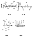
- Such optical modulator will be driven by a combination of two sinusoidal electrical voltages one at some frequency f clock and the second at the third harmonic of that frequency 3f clock. These two sinusoidal electrical voltages are shown on figure 1 ⁇ .
- figure 1 b is shown the electrical signal shape obtained from that combination and which should be applied to an optical modulator possibly biased at the minimum of its transfer curve usually corresponding to its maximum extension.
- FIG 2a and 2b are shown respectively the electrical and optical output of the optical modulator possibly a Mach-Zehnder.
- the optical output is obtained after an electrical to optical conversion.
- the modulator is biased at the minimum of its sinusoidal transfer function with the excitation voltage corresponding to figure 1 b.
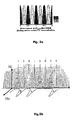
- FIG 3a is shown the final pulses stream after being Phase Mixing-Optical Time Division Multiplexing (PM-OTDM) maintaining cross-polarized bit to bit interleaving.
- PM-OTDM Phase Mixing-Optical Time Division Multiplexing
- FIG 3b is shown again more explicitly the association according to the invention of both the bit-to-bit polarisation interleaving technique and the optical phase modulation technique.
- Figure 3b is a schematic description of such a modulation format in the optical domain separating the two axis of the light polarisation TE and TM and with mark "0" and " ⁇ " for coding the optical phase.
- FIG 4 and 5 are shown two different embodiments of a transmitter according to the invention.
- the continuous wavelengths are divided in two part using a polarisation separating coupler (PSC).
- Mod 1 and Mod 2 are driven at e.g. 20 Gbit/s only with already commercial available drivers producing enough large peak to peak swing voltage well-matched to actual broadband modulators for data coding in NRZ format.
- the multiplexing electronics is only at 20 Gbit/s which allows improved low cost technology with high integration efficiency and ensuring better control of power consumption.
- the second stage of the transmitter as shown on figure 4 is devoted to the format conversion.
- the Mod 3 and Mod 4 are driven only using narrow band amplifier at e.g. 10 GHz and 30 GHz.
- the output amplitude should be two times the voltage of the used optical modulator like a LiNbO 3 Mach-Zehnder modulator (typically 8V).
- FIG 5 On figure 5 is shown a second embodiment of a transmitter according to the invention.
- the number of optical modulator is minimized. This is obtained by applying the combination of the two sinusoidal electrical voltages at frequency f and 3f on a first modulator Mod 0 provided with continuous wavelengths and only afterwards splitting such obtained optical pulse stream using the PSC.
- two optical pulse stream defined by a different polarisation state possibly orthogonal (TE, TM) will be forwarded through a different optical path comprising each a modulator respectively Mod 1 and Mod 2.
- Latter are used to insert the bit-to-bit coding.
- An additional optical delay line ODL is required on one of the two optical paths to be able to interleave precisely the two obtained data streams at e.g. 20 Gbit/s. This ODL is not required in the first scheme (figure 4) taken into account the possibility to adjust each electronic signal (data or clock) using electrical delay line.
- the combination of the two techniques bit-to-bit polarisation interleaving and alternated phase modulation reduce the intra-channel impairments.
- the optical spectrum of such a format (33% of final bit duration) is narrower than classical RZ modulation scheme (50% of bit duration) or even than CS-RZ format. In such a way, nonlinear effects as FWM or crosstalk will be significantly reduced which automatically increase efficiency of DWDM transmission.
Landscapes
- Physics & Mathematics (AREA)
- Electromagnetism (AREA)
- Engineering & Computer Science (AREA)
- Computer Networks & Wireless Communication (AREA)
- Signal Processing (AREA)
- Optics & Photonics (AREA)
- Optical Communication System (AREA)
Abstract
Description
- Fig. 1a and 1b
- are diagrams of voltage excitation to be used for the optical modulator according to the invention;
- Fig. 2a and 2b
- are diagrams of the respectively electrical and optical output of the optical modulator according to the invention;
- Fig 3a and 3b
- are diagrams of optical pulse streams according to the invention;
- Fig. 4
- is a schematic view of a transmitter according to an embodiment of the invention;
- Fig. 5
- is a schematic view of another embodiment of the transmitter according to the invention.
Claims (10)
- A method for processing optical signals to be transmitted through an optical transmission line using optical pulse stream with a carrier suppressed return to zero format to be obtained from at least an optical modulator, the method being characterised by driving the optical modulator with a combination of two sinusoidal electrical voltages, one at some frequency f and the second one at the third harmonic 3f of such frequency.
- The method according to claim 1 characterised by biasing the optical modulator at the minimum of its sinusoidal transfer function with the excitation voltage obtained from that combination of the two sinusoidal electrical voltages.
- The method according to claim 1 or 2 characterised by the achievement of a final optical pulse stream defined by carrier suppressed return to zero pulses having a width of approximately 33% of bit duration.
- The method according to claim 1 or 2 characterised by interleaving at least two such optical pulse streams differing in their polarisation state to give an optical pulse stream at frequency almost 2f.
- The method according to claim 4 characterised by applying a bit-to-bit coding to the two optical pulse streams possibly chosen with different polarisation state.
- A transmitter for optical signals to be forwarded through an optical transmission line, the transmitter comprising a circuit with at least an optical modulator for generating an optical pulse stream having a carrier suppressed return to zero format characterised in that the optical modulator is driven by a combination of two sinusoidal electrical voltages, one at some frequency f and the second one at the third harmonic 3f of such frequency.
- The transmitter according to claim 6 characterised in that the optical modulator being biased at the minimum of its sinusoidal transfer function with the excitation voltage obtained from that combination of the two sinusoidal electrical voltages.
- The transmitter according to claim 6 or 7 characterised in that it comprises two optical paths for the generation of two optical pulse streams differing in their polarisation state while each of these optical paths comprises an optical modulator for the insertion of data signal over the transmitted optical light and said optical modulator driven by this combination of the two sinusoidal electrical voltages.
- The transmitter according to claim 6 or 7 characterised in that it comprises a polarisation separating coupler placed after said optical modulator to divide the optical pulse stream into two optical pulse stream with different polarisation state to be transmitted on different optical paths comprising each an optical modulator for the insertion of data signal over the optical pulse stream.
- The transmitter according to claim 8 or 9 characterised in that the two optical paths are converging into a coupler allowing to interleave the two optical pulse streams possibly bit-to-bit.
Priority Applications (4)
| Application Number | Priority Date | Filing Date | Title |
|---|---|---|---|
| AT04290658T ATE424666T1 (en) | 2004-03-11 | 2004-03-11 | METHOD AND DEVICE FOR GENERATING OPTICAL RZ NARROW PULSE WITH CARRIER SUPPRESSION |
| EP04290658A EP1578040B1 (en) | 2004-03-11 | 2004-03-11 | Method and system for generating CS-RZ pulses showing narrow width of bit duration |
| DE602004019755T DE602004019755D1 (en) | 2004-03-11 | 2004-03-11 | Method and apparatus for generating carrier-suppressed RZ optical thin pulses |
| US11/023,427 US7509056B2 (en) | 2004-03-11 | 2004-12-29 | Method and system for generating CS-RZ pulses showing narrow width of bit duration |
Applications Claiming Priority (1)
| Application Number | Priority Date | Filing Date | Title |
|---|---|---|---|
| EP04290658A EP1578040B1 (en) | 2004-03-11 | 2004-03-11 | Method and system for generating CS-RZ pulses showing narrow width of bit duration |
Publications (2)
| Publication Number | Publication Date |
|---|---|
| EP1578040A1 true EP1578040A1 (en) | 2005-09-21 |
| EP1578040B1 EP1578040B1 (en) | 2009-03-04 |
Family
ID=34833786
Family Applications (1)
| Application Number | Title | Priority Date | Filing Date |
|---|---|---|---|
| EP04290658A Expired - Lifetime EP1578040B1 (en) | 2004-03-11 | 2004-03-11 | Method and system for generating CS-RZ pulses showing narrow width of bit duration |
Country Status (4)
| Country | Link |
|---|---|
| US (1) | US7509056B2 (en) |
| EP (1) | EP1578040B1 (en) |
| AT (1) | ATE424666T1 (en) |
| DE (1) | DE602004019755D1 (en) |
Families Citing this family (3)
| Publication number | Priority date | Publication date | Assignee | Title |
|---|---|---|---|---|
| US20040057734A1 (en) * | 2002-09-25 | 2004-03-25 | Lucent Technologies, Inc. | Method and system for reducing transmission penalties associated with ghost pulses |
| US7643760B1 (en) * | 2006-03-03 | 2010-01-05 | University Of Central Florida Research Foundation, Inc. | Direct detection differential polarization-phase-shift keying for high spectral efficiency optical communication |
| TW200937092A (en) * | 2008-02-22 | 2009-09-01 | Univ Nat Chiao Tung | Photoelectric modulation device generating optical signal of frequency multiplication and modulation method thereof |
Citations (2)
| Publication number | Priority date | Publication date | Assignee | Title |
|---|---|---|---|---|
| EP1309110A1 (en) | 2001-11-05 | 2003-05-07 | Agilent Technologies, Inc. (a Delaware corporation) | Method and system for generating narrow optical pulses |
| US20030189745A1 (en) * | 2002-04-05 | 2003-10-09 | Nobuhiko Kikuchi | Optical single sideband transmitter |
Family Cites Families (11)
| Publication number | Priority date | Publication date | Assignee | Title |
|---|---|---|---|---|
| US7010231B1 (en) * | 1997-08-04 | 2006-03-07 | Cisco Photonics Italy S.R.L. | System and method of high-speed transmission and appropriate transmission apparatus |
| IT1296646B1 (en) * | 1997-12-16 | 1999-07-14 | Cselt Centro Studi Lab Telecom | OPTO-ELECTRONIC CIRCUIT DIVIDER OF FREQUENCY AND RELATED PROCEDURE OF USE. |
| US6950611B2 (en) * | 2000-03-08 | 2005-09-27 | Fitel Usa Corp. | In-line polarization monitoring and control in lightwave communication systems |
| US20020003641A1 (en) * | 2000-05-08 | 2002-01-10 | Hall Katherine L. | Polarization division multiplexer |
| US20020141027A1 (en) * | 2001-02-20 | 2002-10-03 | Lagasse Michael J. | Variable pulse width optical pulse generation with superposed multiple frequency drive |
| GB2372830B (en) * | 2001-03-02 | 2003-05-21 | Marconi Caswell Ltd | Electro-optic gating arrangement with improved duty cycle |
| US7330666B1 (en) * | 2003-01-31 | 2008-02-12 | Ciena Corporation | Method and apparatus for controlling modulator phase alignment in a transmitter of an optical communications system |
| JP3892326B2 (en) * | 2002-03-26 | 2007-03-14 | 富士通株式会社 | Control device for optical modulator |
| US20040057734A1 (en) * | 2002-09-25 | 2004-03-25 | Lucent Technologies, Inc. | Method and system for reducing transmission penalties associated with ghost pulses |
| US6721081B1 (en) * | 2002-09-26 | 2004-04-13 | Corning Incorporated | Variable duty cycle optical pulses |
| US7266306B1 (en) * | 2003-10-03 | 2007-09-04 | Nortel Networks Limited | Method for optical carrier suppression and quadrature control |
-
2004
- 2004-03-11 EP EP04290658A patent/EP1578040B1/en not_active Expired - Lifetime
- 2004-03-11 DE DE602004019755T patent/DE602004019755D1/en not_active Expired - Lifetime
- 2004-03-11 AT AT04290658T patent/ATE424666T1/en not_active IP Right Cessation
- 2004-12-29 US US11/023,427 patent/US7509056B2/en active Active
Patent Citations (2)
| Publication number | Priority date | Publication date | Assignee | Title |
|---|---|---|---|---|
| EP1309110A1 (en) | 2001-11-05 | 2003-05-07 | Agilent Technologies, Inc. (a Delaware corporation) | Method and system for generating narrow optical pulses |
| US20030189745A1 (en) * | 2002-04-05 | 2003-10-09 | Nobuhiko Kikuchi | Optical single sideband transmitter |
Non-Patent Citations (2)
| Title |
|---|
| A. HIRANO: "40 Gbit/s L-band transmission experiment using SPM- tolerant carrier-suppressed RZ format", ELEC. LETTERS, vol. 35, 9 December 1999 (1999-12-09), pages 2213, XP006013072, DOI: doi:10.1049/el:19991499 |
| HIRANO A ET AL: "40 Gbit/s L-band transmission experiment using SPM-tolerant carrier-suppressed RZ format", ELECTRONICS LETTERS, IEE STEVENAGE, GB, vol. 35, no. 25, 9 December 1999 (1999-12-09), pages 2213 - 2215, XP006013072, ISSN: 0013-5194 * |
Also Published As
| Publication number | Publication date |
|---|---|
| US20050201760A1 (en) | 2005-09-15 |
| ATE424666T1 (en) | 2009-03-15 |
| DE602004019755D1 (en) | 2009-04-16 |
| EP1578040B1 (en) | 2009-03-04 |
| US7509056B2 (en) | 2009-03-24 |
Similar Documents
| Publication | Publication Date | Title |
|---|---|---|
| EP0977382B1 (en) | Optical transmission system | |
| US7474859B2 (en) | Versatile compact transmitter for generation of advanced modulation formats | |
| JP3371857B2 (en) | Optical transmission equipment | |
| US8577224B2 (en) | Optical shaping for amplification in a semiconductor optical amplifier | |
| EP1404036B1 (en) | Duobinary optical transmission apparatus | |
| US6842125B2 (en) | Unipolar electrical to CSRZ optical converter | |
| JP3984220B2 (en) | Duobinary optical transmission equipment | |
| KR100492971B1 (en) | Duobinary optical transmitter | |
| US20040076439A1 (en) | Optical transmission system | |
| EP1424795B1 (en) | Optical transmission system using optical phase modulator | |
| JP4053473B2 (en) | Optical transmitter | |
| US20060204162A1 (en) | Device for mach-zehnder modulator bias control for duobinary optical transmission and associated system and method | |
| US20050105916A1 (en) | Optical transmitter for generating duobinary CSRZ and CSRZ-DPSK optical signals for use in optical communication system | |
| EP1578040B1 (en) | Method and system for generating CS-RZ pulses showing narrow width of bit duration | |
| US7224907B2 (en) | Duobinary optical transmission apparatus | |
| EP1515461B1 (en) | Duobinary optical transmitter | |
| CN1497895A (en) | optical transmission system | |
| WO2009124471A1 (en) | Methods and systems for optical communication | |
| KR100469740B1 (en) | Duobinary optical transmitter | |
| JP3964856B2 (en) | Optical transmitter | |
| EP1716650B1 (en) | System for generating optical return-to-zero signals with alternating bi-phase shift | |
| EP1473856B1 (en) | Duobinary optical transmission apparatus | |
| van den Borne et al. | A robust modulation format for 42.8-Gbit/s long-haul transmission: RZ-DPSK or RZ-DQPSK? | |
| Vassilieva et al. | New Nonlinear Tolerant Phase Modulation Based OTDM Scheme with Low Insertion Loss for 80Gb/s Transmission | |
| He et al. | Duobinary RZ and Dark RZ signals generation using only one differential Mach-Zehnder modulator |
Legal Events
| Date | Code | Title | Description |
|---|---|---|---|
| PUAI | Public reference made under article 153(3) epc to a published international application that has entered the european phase |
Free format text: ORIGINAL CODE: 0009012 |
|
| 17P | Request for examination filed |
Effective date: 20041208 |
|
| AK | Designated contracting states |
Kind code of ref document: A1 Designated state(s): AT BE BG CH CY CZ DE DK EE ES FI FR GB GR HU IE IT LI LU MC NL PL PT RO SE SI SK TR |
|
| AX | Request for extension of the european patent |
Extension state: AL LT LV MK |
|
| AKX | Designation fees paid |
Designated state(s): AT BE BG CH CY CZ DE DK EE ES FI FR GB GR HU IE IT LI LU MC NL PL PT RO SE SI SK TR |
|
| RAP1 | Party data changed (applicant data changed or rights of an application transferred) |
Owner name: ALCATEL LUCENT |
|
| GRAP | Despatch of communication of intention to grant a patent |
Free format text: ORIGINAL CODE: EPIDOSNIGR1 |
|
| GRAS | Grant fee paid |
Free format text: ORIGINAL CODE: EPIDOSNIGR3 |
|
| GRAA | (expected) grant |
Free format text: ORIGINAL CODE: 0009210 |
|
| AK | Designated contracting states |
Kind code of ref document: B1 Designated state(s): AT BE BG CH CY CZ DE DK EE ES FI FR GB GR HU IE IT LI LU MC NL PL PT RO SE SI SK TR |
|
| REG | Reference to a national code |
Ref country code: GB Ref legal event code: FG4D |
|
| REG | Reference to a national code |
Ref country code: CH Ref legal event code: EP |
|
| REG | Reference to a national code |
Ref country code: IE Ref legal event code: FG4D |
|
| REF | Corresponds to: |
Ref document number: 602004019755 Country of ref document: DE Date of ref document: 20090416 Kind code of ref document: P |
|
| PG25 | Lapsed in a contracting state [announced via postgrant information from national office to epo] |
Ref country code: NL Free format text: LAPSE BECAUSE OF FAILURE TO SUBMIT A TRANSLATION OF THE DESCRIPTION OR TO PAY THE FEE WITHIN THE PRESCRIBED TIME-LIMIT Effective date: 20090304 Ref country code: FI Free format text: LAPSE BECAUSE OF FAILURE TO SUBMIT A TRANSLATION OF THE DESCRIPTION OR TO PAY THE FEE WITHIN THE PRESCRIBED TIME-LIMIT Effective date: 20090304 Ref country code: SI Free format text: LAPSE BECAUSE OF FAILURE TO SUBMIT A TRANSLATION OF THE DESCRIPTION OR TO PAY THE FEE WITHIN THE PRESCRIBED TIME-LIMIT Effective date: 20090304 |
|
| NLV1 | Nl: lapsed or annulled due to failure to fulfill the requirements of art. 29p and 29m of the patents act | ||
| PG25 | Lapsed in a contracting state [announced via postgrant information from national office to epo] |
Ref country code: PL Free format text: LAPSE BECAUSE OF FAILURE TO SUBMIT A TRANSLATION OF THE DESCRIPTION OR TO PAY THE FEE WITHIN THE PRESCRIBED TIME-LIMIT Effective date: 20090304 Ref country code: AT Free format text: LAPSE BECAUSE OF FAILURE TO SUBMIT A TRANSLATION OF THE DESCRIPTION OR TO PAY THE FEE WITHIN THE PRESCRIBED TIME-LIMIT Effective date: 20090304 Ref country code: SE Free format text: LAPSE BECAUSE OF FAILURE TO SUBMIT A TRANSLATION OF THE DESCRIPTION OR TO PAY THE FEE WITHIN THE PRESCRIBED TIME-LIMIT Effective date: 20090604 |
|
| PG25 | Lapsed in a contracting state [announced via postgrant information from national office to epo] |
Ref country code: BE Free format text: LAPSE BECAUSE OF FAILURE TO SUBMIT A TRANSLATION OF THE DESCRIPTION OR TO PAY THE FEE WITHIN THE PRESCRIBED TIME-LIMIT Effective date: 20090304 |
|
| PG25 | Lapsed in a contracting state [announced via postgrant information from national office to epo] |
Ref country code: EE Free format text: LAPSE BECAUSE OF FAILURE TO SUBMIT A TRANSLATION OF THE DESCRIPTION OR TO PAY THE FEE WITHIN THE PRESCRIBED TIME-LIMIT Effective date: 20090304 Ref country code: MC Free format text: LAPSE BECAUSE OF NON-PAYMENT OF DUE FEES Effective date: 20090331 Ref country code: CZ Free format text: LAPSE BECAUSE OF FAILURE TO SUBMIT A TRANSLATION OF THE DESCRIPTION OR TO PAY THE FEE WITHIN THE PRESCRIBED TIME-LIMIT Effective date: 20090304 Ref country code: PT Free format text: LAPSE BECAUSE OF FAILURE TO SUBMIT A TRANSLATION OF THE DESCRIPTION OR TO PAY THE FEE WITHIN THE PRESCRIBED TIME-LIMIT Effective date: 20090819 Ref country code: ES Free format text: LAPSE BECAUSE OF FAILURE TO SUBMIT A TRANSLATION OF THE DESCRIPTION OR TO PAY THE FEE WITHIN THE PRESCRIBED TIME-LIMIT Effective date: 20090615 |
|
| REG | Reference to a national code |
Ref country code: CH Ref legal event code: PL |
|
| PG25 | Lapsed in a contracting state [announced via postgrant information from national office to epo] |
Ref country code: RO Free format text: LAPSE BECAUSE OF FAILURE TO SUBMIT A TRANSLATION OF THE DESCRIPTION OR TO PAY THE FEE WITHIN THE PRESCRIBED TIME-LIMIT Effective date: 20090304 Ref country code: SK Free format text: LAPSE BECAUSE OF FAILURE TO SUBMIT A TRANSLATION OF THE DESCRIPTION OR TO PAY THE FEE WITHIN THE PRESCRIBED TIME-LIMIT Effective date: 20090304 |
|
| REG | Reference to a national code |
Ref country code: IE Ref legal event code: MM4A |
|
| PLBE | No opposition filed within time limit |
Free format text: ORIGINAL CODE: 0009261 |
|
| STAA | Information on the status of an ep patent application or granted ep patent |
Free format text: STATUS: NO OPPOSITION FILED WITHIN TIME LIMIT |
|
| PG25 | Lapsed in a contracting state [announced via postgrant information from national office to epo] |
Ref country code: IE Free format text: LAPSE BECAUSE OF NON-PAYMENT OF DUE FEES Effective date: 20090311 Ref country code: DK Free format text: LAPSE BECAUSE OF FAILURE TO SUBMIT A TRANSLATION OF THE DESCRIPTION OR TO PAY THE FEE WITHIN THE PRESCRIBED TIME-LIMIT Effective date: 20090304 Ref country code: CH Free format text: LAPSE BECAUSE OF NON-PAYMENT OF DUE FEES Effective date: 20090331 Ref country code: LI Free format text: LAPSE BECAUSE OF NON-PAYMENT OF DUE FEES Effective date: 20090331 Ref country code: BG Free format text: LAPSE BECAUSE OF FAILURE TO SUBMIT A TRANSLATION OF THE DESCRIPTION OR TO PAY THE FEE WITHIN THE PRESCRIBED TIME-LIMIT Effective date: 20090604 |
|
| 26N | No opposition filed |
Effective date: 20091207 |
|
| PG25 | Lapsed in a contracting state [announced via postgrant information from national office to epo] |
Ref country code: GR Free format text: LAPSE BECAUSE OF FAILURE TO SUBMIT A TRANSLATION OF THE DESCRIPTION OR TO PAY THE FEE WITHIN THE PRESCRIBED TIME-LIMIT Effective date: 20090605 |
|
| PG25 | Lapsed in a contracting state [announced via postgrant information from national office to epo] |
Ref country code: IT Free format text: LAPSE BECAUSE OF FAILURE TO SUBMIT A TRANSLATION OF THE DESCRIPTION OR TO PAY THE FEE WITHIN THE PRESCRIBED TIME-LIMIT Effective date: 20090304 |
|
| PG25 | Lapsed in a contracting state [announced via postgrant information from national office to epo] |
Ref country code: LU Free format text: LAPSE BECAUSE OF NON-PAYMENT OF DUE FEES Effective date: 20090311 |
|
| PG25 | Lapsed in a contracting state [announced via postgrant information from national office to epo] |
Ref country code: HU Free format text: LAPSE BECAUSE OF FAILURE TO SUBMIT A TRANSLATION OF THE DESCRIPTION OR TO PAY THE FEE WITHIN THE PRESCRIBED TIME-LIMIT Effective date: 20090905 |
|
| PG25 | Lapsed in a contracting state [announced via postgrant information from national office to epo] |
Ref country code: TR Free format text: LAPSE BECAUSE OF FAILURE TO SUBMIT A TRANSLATION OF THE DESCRIPTION OR TO PAY THE FEE WITHIN THE PRESCRIBED TIME-LIMIT Effective date: 20090304 |
|
| PG25 | Lapsed in a contracting state [announced via postgrant information from national office to epo] |
Ref country code: CY Free format text: LAPSE BECAUSE OF FAILURE TO SUBMIT A TRANSLATION OF THE DESCRIPTION OR TO PAY THE FEE WITHIN THE PRESCRIBED TIME-LIMIT Effective date: 20090304 |
|
| REG | Reference to a national code |
Ref country code: FR Ref legal event code: GC Effective date: 20131018 |
|
| REG | Reference to a national code |
Ref country code: FR Ref legal event code: RG Effective date: 20141016 |
|
| REG | Reference to a national code |
Ref country code: FR Ref legal event code: PLFP Year of fee payment: 12 |
|
| REG | Reference to a national code |
Ref country code: FR Ref legal event code: CA Effective date: 20150521 |
|
| REG | Reference to a national code |
Ref country code: FR Ref legal event code: CA Effective date: 20150521 |
|
| REG | Reference to a national code |
Ref country code: FR Ref legal event code: PLFP Year of fee payment: 13 |
|
| PGFP | Annual fee paid to national office [announced via postgrant information from national office to epo] |
Ref country code: FR Payment date: 20160321 Year of fee payment: 13 Ref country code: GB Payment date: 20160321 Year of fee payment: 13 |
|
| PGFP | Annual fee paid to national office [announced via postgrant information from national office to epo] |
Ref country code: DE Payment date: 20160330 Year of fee payment: 13 |
|
| REG | Reference to a national code |
Ref country code: DE Ref legal event code: R119 Ref document number: 602004019755 Country of ref document: DE |
|
| GBPC | Gb: european patent ceased through non-payment of renewal fee |
Effective date: 20170311 |
|
| REG | Reference to a national code |
Ref country code: FR Ref legal event code: ST Effective date: 20171130 |
|
| PG25 | Lapsed in a contracting state [announced via postgrant information from national office to epo] |
Ref country code: FR Free format text: LAPSE BECAUSE OF NON-PAYMENT OF DUE FEES Effective date: 20170331 Ref country code: DE Free format text: LAPSE BECAUSE OF NON-PAYMENT OF DUE FEES Effective date: 20171003 |
|
| PG25 | Lapsed in a contracting state [announced via postgrant information from national office to epo] |
Ref country code: GB Free format text: LAPSE BECAUSE OF NON-PAYMENT OF DUE FEES Effective date: 20170311 |