EP1574514A1 - Organometal complex, electroluminescent element containing the organometal complex and luminescent device including the electroluminescent element - Google Patents
Organometal complex, electroluminescent element containing the organometal complex and luminescent device including the electroluminescent element Download PDFInfo
- Publication number
- EP1574514A1 EP1574514A1 EP03778761A EP03778761A EP1574514A1 EP 1574514 A1 EP1574514 A1 EP 1574514A1 EP 03778761 A EP03778761 A EP 03778761A EP 03778761 A EP03778761 A EP 03778761A EP 1574514 A1 EP1574514 A1 EP 1574514A1
- Authority
- EP
- European Patent Office
- Prior art keywords
- light
- electroluminescent device
- group
- organometallic complex
- electroluminescent
- Prior art date
- Legal status (The legal status is an assumption and is not a legal conclusion. Google has not performed a legal analysis and makes no representation as to the accuracy of the status listed.)
- Withdrawn
Links
- 0 *C(c1cc(*)c(*)c(*)c1*)=O Chemical compound *C(c1cc(*)c(*)c(*)c1*)=O 0.000 description 2
Images


Classifications
-
- C—CHEMISTRY; METALLURGY
- C07—ORGANIC CHEMISTRY
- C07C—ACYCLIC OR CARBOCYCLIC COMPOUNDS
- C07C251/00—Compounds containing nitrogen atoms doubly-bound to a carbon skeleton
- C07C251/02—Compounds containing nitrogen atoms doubly-bound to a carbon skeleton containing imino groups
- C07C251/24—Compounds containing nitrogen atoms doubly-bound to a carbon skeleton containing imino groups having carbon atoms of imino groups bound to carbon atoms of six-membered aromatic rings
-
- C—CHEMISTRY; METALLURGY
- C09—DYES; PAINTS; POLISHES; NATURAL RESINS; ADHESIVES; COMPOSITIONS NOT OTHERWISE PROVIDED FOR; APPLICATIONS OF MATERIALS NOT OTHERWISE PROVIDED FOR
- C09K—MATERIALS FOR MISCELLANEOUS APPLICATIONS, NOT PROVIDED FOR ELSEWHERE
- C09K11/00—Luminescent materials, e.g. electroluminescent or chemiluminescent
- C09K11/06—Luminescent materials, e.g. electroluminescent or chemiluminescent containing organic luminescent materials
-
- C—CHEMISTRY; METALLURGY
- C07—ORGANIC CHEMISTRY
- C07F—ACYCLIC, CARBOCYCLIC OR HETEROCYCLIC COMPOUNDS CONTAINING ELEMENTS OTHER THAN CARBON, HYDROGEN, HALOGEN, OXYGEN, NITROGEN, SULFUR, SELENIUM OR TELLURIUM
- C07F15/00—Compounds containing elements of Groups 8, 9, 10 or 18 of the Periodic Table
- C07F15/0006—Compounds containing elements of Groups 8, 9, 10 or 18 of the Periodic Table compounds of the platinum group
- C07F15/0033—Iridium compounds
-
- H—ELECTRICITY
- H05—ELECTRIC TECHNIQUES NOT OTHERWISE PROVIDED FOR
- H05B—ELECTRIC HEATING; ELECTRIC LIGHT SOURCES NOT OTHERWISE PROVIDED FOR; CIRCUIT ARRANGEMENTS FOR ELECTRIC LIGHT SOURCES, IN GENERAL
- H05B33/00—Electroluminescent light sources
- H05B33/12—Light sources with substantially two-dimensional [2D] radiating surfaces
- H05B33/14—Light sources with substantially two-dimensional [2D] radiating surfaces characterised by the chemical or physical composition or the arrangement of the electroluminescent material, or by the simultaneous addition of the electroluminescent material in or onto the light source
-
- C—CHEMISTRY; METALLURGY
- C09—DYES; PAINTS; POLISHES; NATURAL RESINS; ADHESIVES; COMPOSITIONS NOT OTHERWISE PROVIDED FOR; APPLICATIONS OF MATERIALS NOT OTHERWISE PROVIDED FOR
- C09K—MATERIALS FOR MISCELLANEOUS APPLICATIONS, NOT PROVIDED FOR ELSEWHERE
- C09K2211/00—Chemical nature of organic luminescent or tenebrescent compounds
- C09K2211/10—Non-macromolecular compounds
- C09K2211/1003—Carbocyclic compounds
- C09K2211/1007—Non-condensed systems
-
- C—CHEMISTRY; METALLURGY
- C09—DYES; PAINTS; POLISHES; NATURAL RESINS; ADHESIVES; COMPOSITIONS NOT OTHERWISE PROVIDED FOR; APPLICATIONS OF MATERIALS NOT OTHERWISE PROVIDED FOR
- C09K—MATERIALS FOR MISCELLANEOUS APPLICATIONS, NOT PROVIDED FOR ELSEWHERE
- C09K2211/00—Chemical nature of organic luminescent or tenebrescent compounds
- C09K2211/18—Metal complexes
- C09K2211/185—Metal complexes of the platinum group, i.e. Os, Ir, Pt, Ru, Rh or Pd
-
- Y—GENERAL TAGGING OF NEW TECHNOLOGICAL DEVELOPMENTS; GENERAL TAGGING OF CROSS-SECTIONAL TECHNOLOGIES SPANNING OVER SEVERAL SECTIONS OF THE IPC; TECHNICAL SUBJECTS COVERED BY FORMER USPC CROSS-REFERENCE ART COLLECTIONS [XRACs] AND DIGESTS
- Y10—TECHNICAL SUBJECTS COVERED BY FORMER USPC
- Y10S—TECHNICAL SUBJECTS COVERED BY FORMER USPC CROSS-REFERENCE ART COLLECTIONS [XRACs] AND DIGESTS
- Y10S428/00—Stock material or miscellaneous articles
- Y10S428/917—Electroluminescent
Definitions
- the present invention relates to a compound that is able to convert a triplet excited state into light emission.
- the present invention also relates to an electroluminescent device that has an anode, a cathode, and a layer including an organic compound (hereinafter, referred to as "electroluminescent layer") from which light emission is obtained by applying electric field, where the electroluminescent layer includes a compound that is able to convert a triplet excited state into light emission, and a light-emitting device using the electroluminescent device.
- an organic compound organic compound
- the organic compound gets to have energy (an excited state). Trough this excited state, various photochemical reactions may be developed or light emission (luminescence) may be generated, and various applications have been tried.
- an electroluminescent device a device that emits light by applying electric field
- the emission mechanism of an electroluminescent device is a carrier injection type.
- an electron injected from a cathode and a hole injected from an anode are recombined in the electroluminescent layer to form a molecule in an excited state (hereinafter, referred to as an exited molecule), and energy is released to emit light while the excited molecule moves back toward the ground state.
- the electroluminescent layer is generally formed of a thin film about below 1 ⁇ m. Further, since the foregoing electroluminescent device is a self-luminous device, where the electroluminescent layer itself emits light, a backlight that is used for a conventional liquid crystal display is unnecessary. Therefore, it is a great advantage that it is possible to be manufactured to have significantly a thin thickness and a lightweight.
- the time from an injection of carriers to their recombination is about several ten nanoseconds considering the carrier mobility of the electroluminescent layer. Even when processes from the recombination of the carriers to light emission are included, only time on the microsecond time scale is required to reach light emission. Thus, the fairly high response speed is also one of the features.
- the foregoing electroluminescent device is a carrier injection type light-emitting device, driving by DC voltage is possible, and it is unlikely that a noise is generated.
- the driving voltage an uniform ultra thin film with a thickness of approximately 100nm is first used as the electroluminescent layer, a material for an electrode is also selected to reduce a carrier injection barrier against the electroluminescent layer, and a heterostructure (two-layer structure) is additionally introduced. Accordingly, a sufficient luminance of 100 cd/m 2 can be obtained at 5.5V (refer to Non-Patent Document 1, for example).
- the electroluminescent device has been attracting attention as a next-generation flat panel display in terms of the features such as the thin thickness and the lightweight, the high speed response, and the low DC voltage drive.
- relatively favorable visibility can be obtained since the electroluminescent device is a self-luminous device that has a wide viewing angle, and the electroluminescent device is considered to be effective as the device for a display screen of a portable device.
- generated light is not all coupled out to the outside, and it is not possible to take a portion of the light out due to inherent refractive indexes of a constituent material of an electroluminescent device and a material of a substrate.
- the ratio of light taken out to the outside to generated light is referred at as a light-extraction efficiency, it is said that the light-extraction efficiency is only about 20 % in an electroluminescent device that has a glass substrate.
- Non-Patent Document 3 (Non-Patent Document 3)
- Non-Patent Document 4 (Non-Patent Document 4)
- a porphyrin complex that has platinum as a central metal and an organometallic complex that has iridium as a central metal are respectively used in Non-Patent Document 3 and in Non-Patent Document 4, and both of the complexes are of a phosphorescent material that has a third-series transition element introduced as a central metal, which includes one that well exceeds the foregoing theoretical limit 5 % of the external quantum efficiency.
- an electroluminescent device using a phosphorescent material can achieve a higher external efficiency than conventional one. Then, as the external efficiency is higher, the luminance is improved.
- an electroluminescent device using a phosphorescent material is considered to occupy an important position in a future development as a means for accomplishing luminescence with a high luminance and a high luminance efficiency.
- a phosphorescent material is useful for being applied to electroluminescent devices, which is expected. However, it is still the case that the number thereof is small.
- the iridium complex that is used in Non-Paten Document 4 is one of organometallic complexes referred to as an orthometalated complex. Since this complex has a phosphorescence lifetime of several hundreds nanoseconds and a high phosphorescence quantum yield, the decrease in efficiency associated with an increase in luminance is small as compared to the porphyrin complex. From that viewpoint, the foregoing organometallic complex using the heavy metal is one of guidelines for synthesizing a phosphorescent material.
- an electroluminescent device has been actively developed for being applied to displays. Above all, the development of a device that can emit white light has been distinctly attracting attention. This is because full color display is possible when a color filter is attached to a display device, in addition to applications as mono-color display and lighting such as a backlight.
- a method such as a method of mixing materials that respectively emit R (red), G (green), and B (blue) to form a thin film, a method of laminating layers that respectively emit R (red), G (green), and B (blue), or a method of combining complementary colors (a blue-green color and an orange color, for example) (refer to Non-Patent Document 5, for example) is considered.
- a plurality of luminescent materials that have different emission wavelengths are needed in any case in order to obtain a spectrum of white light, there is a problem that a driving voltage is increased.
- a hole blocking layer since it is necessary to combine a hole blocking layer in order to obtain a high luminous efficiency from an electroluminescent device using a phosphorescent material, a quite complicated device structure is required.
- Non-Patent Document 5 (Non-Patent Document 5)
- the light-emitting device in the specification indicates a light-emitting device and an image display device that use an electroluminescent device.
- a module that has a connecter such as an anisotropic conductive film (EPC: Flexible Printed Circuit) or TAB (Tape Automated Bonding) attached to an electroluminescent device a module that has a TAB tape or a TCP (Tape Carrier Package) attached, a module that has a printed wiring board provided at the tip of a TAB tape or a TCP, and a module that has an electroluminescent device directly mounted with an IC (integrated circuit) by a COG (Chip On Glass) method are all included in the light-emitting device.
- a connecter such as an anisotropic conductive film (EPC: Flexible Printed Circuit) or TAB (Tape Automated Bonding) attached to an electroluminescent device
- TAB tape or a TCP Tape Carrier Package
- a module that has a printed wiring board provided at the tip of a TAB tape or a TCP a module that has an electroluminescent device directly mounted with an IC (
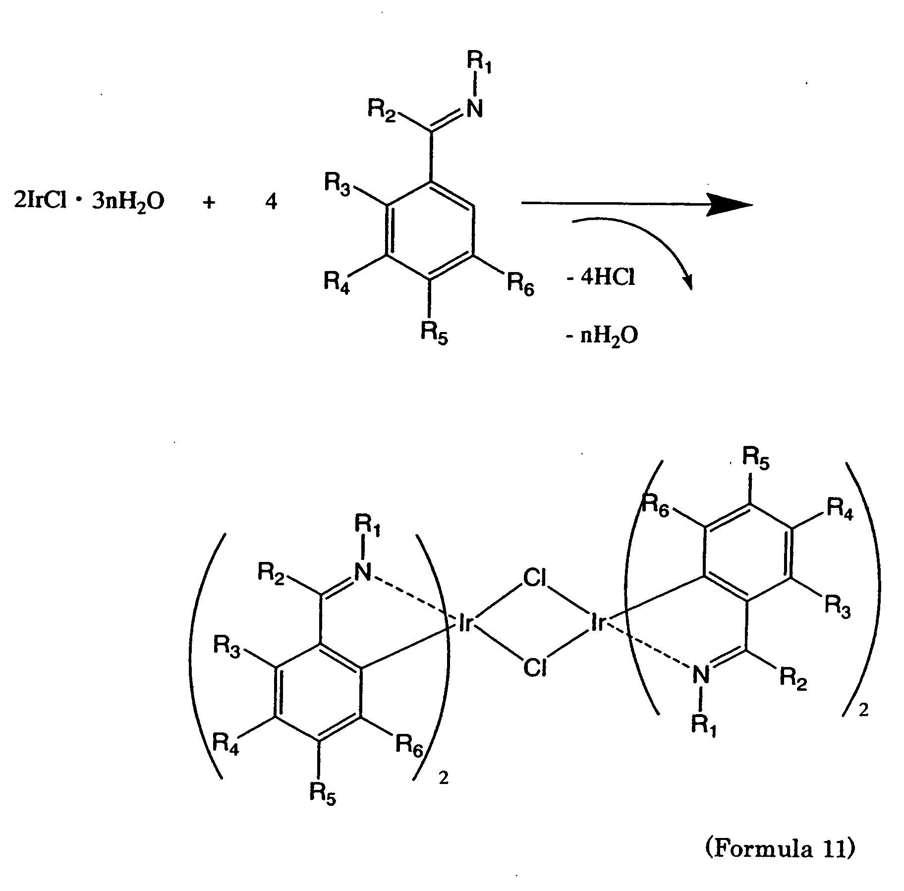
- the inventors have focused on an organometallic compound that has an element of Group 9 or an element of Group 10 as a center, which can be formed in the case of using a ligand shown by the following general formula 1.
- a complex represented by the following general formula 2, which is synthesized by orthometallation of the ligand of the general formula 1, has both components of fluorescence and phosphorescence of in the region of visible light. Since emission wavelengths of fluorescence and phosphorescence of this complex are observed respectively in the side of shorter wavelengths and in the side of longer wavelengths, it is a feature to be a white or whitish lighting color.
- R 1 is an alkyl group, an aryl group, a substituted aryl group, a heterocyclic group or a substituted heterocyclic group
- R 2 is hydrogen, an alkyl group, an aryl group, a substituted aryl group, a heterocyclic group, or a substituted heterocyclic group
- R 3 , R 4 , R 5 , and R 6 may be identical or different, and are individually hydrogen, halogen, an alkyl group, an alkoxyl group, an aryl group, a substituted aryl group, a heterocyclic group, or a substituted heterocyclic group
- M is an element of Group 9 or an element of Group 10
- L is a monoanionic ligand having a ⁇ -diketone structure, a monoanionic bidentate ligand having a carboxyl group, or a monoanionic bidentate
- the central metal M is iridium or platinum in the aforementioned general formula.
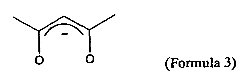
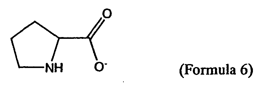
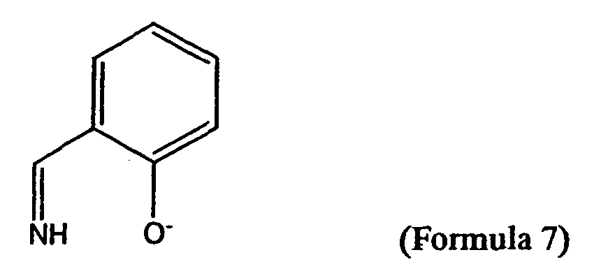
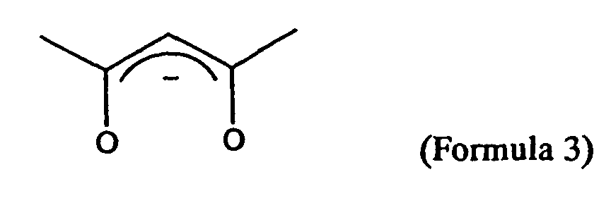
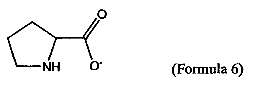
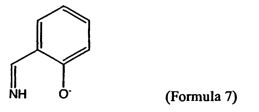
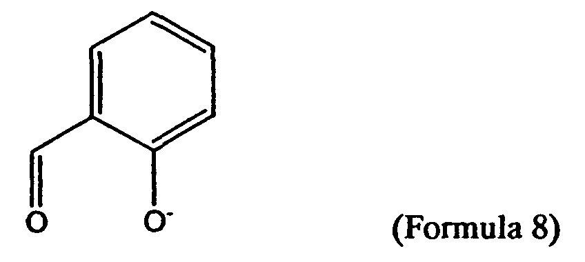
- any of monoanionic ligands shown by structure formulas 3 to 9 below is preferable although the ligand L is any of a monoanionic ligand having a ⁇ -diketone structure, a monoanionic bidentate ligand having a carboxyl group, and a monoanionic bidentate ligand having a phenolic hydroxyl group.
- the organometallic complex according to the present invention can convert triplet excitation energy into light emission, an efficient device with white or whitish luminescence becomes possible by applying the organometallic complex to an electroluminescent device, which is quite efficient. Consequently, the present invention also includes an electroluminescent device that uses the organometallic complex according to the present invention.
- the present invention also includes a light-emitting device that uses the organometallic complex according to the present invention.
- a novel organometallic compound can be provided by carrying out the present invention.
- an electroluminescent device that has a high luminous efficiency can be provided by using the organometallic compound to manufacture an electroluminescent device.
- a light-emitting device and an electronic device with low power consumption can be provided by using the organometallic complex to manufacture a light-emitting device and an electronic device.
- the ligand represented by the aforementioned general formula 1 can be synthesized in accordance with the following synthesis scheme 10.
- ligand of the general formula 1 is used to form the organometallic complex according to the present invention (general formula 2).
- a known synthesis method may be used.
- iridium chloride hydrate is used as a raw material to synthesize a chlorine-bridged dinuclear complex first by mixing the iridium chloride hydrate with the ligand of the general formula 1 and refluxing in a nitrogen atmosphere (the following synthesis scheme 11).
- the chlorine bridge is cut with the ligand L to obtain the organometallic complex according to the present invention by mixing the obtained dinuclear complex and a raw material for the ligand L and refluxing in a nitrogen atmosphere (the following synthesis scheme 12).
- the synthesis method of the organometallic complex which is used in the present invention, is not limited to the synthesis method shown above.
- the organometallic complex according to the present invention can be used as a fluorescent and phosphorescent material, it is believed that it is more preferable that the substituent R 2 in the aforementioned general formula 2 is not hydrogen but an electron donating group such as an alkyl group in order to efficiently realize the both components of fluorescence and phosphorescence.
- Embodiment Mode 1 a device structure of an electroluminescent device that invention, a hole injection layer comprising a low molecular weight material, a hole transport layer, a hole blocking layer, and an electron transport layer will be described with reference to Fig. 1.
- Fig. 1 has a structure where a first electrode 101 is formed on a substrate 100, an electroluminescent layer 102 is formed on the first electrode 101, and a second electrode 103 is formed thereon.
- a material that is used for the substrate 100 a material that is used in a conventional electroluminescent device may be used, and a substrate comprising such as glass, quartz, or transparent plastic can be used.
- the first electrode 101 in Embodiment Mode 1 functions as an anode and the second electrode 103 functions as a cathode.
- the first electrode 101 is formed of an anode material, and it is preferable to use a metal, an alloy, an electrically conductive compound, and a mixture of these, which have a large work function (a work function of 4.0 eV or more), as the anode material that can be used here.
- gold As a specific example of the anode material, gold (Au), platinum (Pt), nickel (Ni), tungsten (W), chromium (Cr), molybdenum (Mo), iron (Fe), cobalt (Co), copper (Cu), palladium (Pd), a nitride of a metal material (TiN), or the like can be used in addition to ITO (indium tin oxide) and IZO (indium zinc oxide) of indium oxide mixed with zinc oxide (ZnO) at 2 to 20 [%].
- ITO indium tin oxide
- IZO indium zinc oxide
- a rare-earth metal can be used for the formation in addition to an element belonging to Group 1 or Group 2 of the periodic table of the element, that is, an alkali metal such as Li or Cs, and an alkali earth element such as Mg, Ca, or Sr, and an alloy (Mg:Ag, Al:Li) and a compound (LiF, CsF, CaF 2 ) including these, and it is also possible to further laminate a metal (including an alloy) such as Al, Ag, or ITO for the formation.
- an alkali metal such as Li or Cs
- an alkali earth element such as Mg, Ca, or Sr
- an alloy Mg:Ag, Al:Li
- a compound LiF, CsF, CaF 2
- a thin film of the foregoing anode material and a thin film of the cathode material are formed by evaporation, sputtering, or the like to respectively form the first electrode 101 and the second electrode 103, which preferably have a film thickness of 10 to 500 nm.
- the electroluminescent device Besides, in the electroluminescent device according to the present invention, light generated by recombination of carriers in the electroluminescent layer is emitted from one or both of the first electrode 101 and the second electrode 103 to the outside.
- the first electrode 101 is formed of a translucent material in the case where light is emitted from the side of the first electrode 101 while the second electrode 103 is formed of a translucent material in the case where light is emitted from the side of the second electrode 103.
- the electroluminescent layer 102 uses a single layer, or is formed by laminating a plurality of layer.
- the electroluminescent layer 102 is formed by laminating a hole injection layer 111, a hole transport layer 112, a light-emitting layer 113, a hole blocking layer 114, and an electron transport layer 115.
- a phthalocyanine-based compound As a hole injection material for forming the hole injection layer 111, a phthalocyanine-based compound is efficient.
- phthalocyanine abbreviation: referred to as H 2 -Pc
- copper phthalocyanine abbreviation: referred to as Cu-Pc
- H 2 -Pc phthalocyanine
- Cu-Pc copper phthalocyanine
- an aromatic amine-based (that is, one that has a bond of benzene ring-nitrogen) compound is widely used.
- materials that are used widely for example, in addition to 4, 4' - bis [N - (3 - methylphenyl) - N - phenyl - amino] - biphenyl (abbreviation: TPD), a derivative thereof such as 4, 4' - bis [N - (1 - naphthyl) - N - phenyl - amino] - biphenyl (abbreviation: ⁇ -NPD) and star burst aromatic amine compounds such as 4, 4', 4" - tris (N, N - diphenyl - amino) - triphenylamine (abbreviation: TDATA) and 4, 4', 4" - tris [N - (3 - methylphenyl) - N - phenyl - amino] - triphen
- the light-emitting layer 113 includes the organometallic complex previously shown by the general formula 2, and is formed by co-evaporation of this organometallic complex and a host material.
- a host material a known material can be used, and 4, 4' - bis (N - carbazolyl) - biphenyl (abbreviation: CBP), 2, 2' 2" - (1, 3, 5 - benzenetriyl) - tris [1 - phenyl - 1Hbenzimidazole] (abbreviation: TPBI), and the like can be given.
- a hole blocking material for forming the hole blocking layer 114 bis (2 - methyl - 8 - quinolinolate) - (4 - phenylphenolato)-aluminum (abbreviation: BAlq), 1, 3 - bis [5 - (p - tert - butylphenyl) - 1, 3, 4 - oxadiazole - 2 - yl] benzene (abbreviation: OXD-7), 3 - (4 - tert - butylphenyl) - 4 - phenyl - 5 - (4 - biphenylyl) - 1, 2, 4 - triazole (abbreviation: TAZ), 3 - (4 - tert - butylphenyl) - 4 - (4 - ethylphenyl) - 5 - (4 - biphenylyl) - 1, 2, 4 - triazole (abbreviation: p-EtTAZ
- a metal complex that has a quinoline skeleton or a benzoquinoline skeleton such as tris (8 - quinolinolato) aluminum (abbreviation: Alq 3 ), tris (5 - methyl - 8 - quinolinolato) aluminum (abbreviation: Almq 3 ), or bis (10 - hydroxybenzo[h] - quinolinato) beryllium (abbreviation: BeBq 2 ), and BAlq mentioned above are preferred.
- a metal complex that has an oxazole-based ligand or a thiazole-based ligand such as bis [2 - (2 - hydroxyphenyl) - benzothiazolato] zinc (abbreviation: Zn(BTZ) 2 ) can also be used.
- Zn(BTZ) 2 bis [2 - (2 - hydroxyphenyl) - benzothiazolato] zinc
- PBD a metal complex that has an oxazole-based ligand or a thiazole-based ligand such as bis [2 - (2 - hydroxyphenyl) - benzothiazolato] zinc
- PBD a metal complex that has an oxazole-based ligand or a thiazole-based ligand such as bis [2 - (2 - hydroxyphenyl) - benzothiazolato] zinc
- PBD a metal complex that has an oxazole-based ligand or a
- an electroluminescent device that has the light-emitting layer 113 including the organometallic complex according to the present invention, the hole injection layer 111 comprising the low molecular weight, the hole transport layer 112, the hole blocking layer (hole blocking layer) 114, and the hole transport layer 115.
- the organometallic complex according to the present invention is used as a guest material in the light-emitting layer 113
- the electroluminescent device is the device that has luminescence obtained from the organometallic complex according to the present invention as a lighting color.
- Embodiment Mode 2 a device structure of an electroluminescent device that has a light-emitting layer including an organometallic complex according to the present invention and a hole injection layer comprising a polymer material, which are formed with a wet process, will be described with reference to Fig.2.
- an electroluminescent layer 202 is formed by laminating a plurality of layers, in Embodiment Mode 2, formed by laminating a hole injection layer 211 and a light-emitting layer 212.
- PEDOT polythiophene dioxythiophene
- PSS polystyrene sulfonate
- PVK polyvinyl carbazole
- the light-emitting layer 212 includes the organometallic complex according to the present invention, which is previously shown by the general formula 2, as a guest compound.
- a bipolar material may be used, or a hole transport material and an electron transport material may be mixed alternatively to be bipolar.
- a hole transport polymer compound (PVK, for example) and the aforementioned electron transport material (PBD, for example) are dissolved in the same solvent at 7 : 3 (molar ratio) first, and an appropriate amount of the organometallic complex according to the present invention (approximately 5 wt%) is further added to prepare a solution.
- the light-emitting layer 212 can be obtained by wet application of this solution and baking.
- an electroluminescent device that has the light-emitting layer 212 including the organometallic complex according to the present invention and the hole injection layer 211 comprising the polymer material, which are formed with a wet process.
- the organometallic complex according to the present invention is used as a guest material in the light-emitting layer 212
- the electroluminescent device is a light-emitting device that has luminescence obtained from the organometallic complex according to the present invention as a lighting color.
- the present synthesis example will exemplify a synthesis method of an organometallic complex according to the present invention, represented by the following structure formula 13.
- a ligand represented by the following structure formula 14 was obtained by removing the solvent (umber and oily).
- iridium chloride (IrCl 3 HCl H 2 O and 2.5 equivalents of the structure formula 14 were refluxed in a mixed solvent of 2-ethoxyethanol and water at 3:1 in a nitrogen atmosphere for 16 hours to obtain a dinuclear complex of the flowing structure formula 15.
- the obtained powder was filtered, and subjected to air drying after washing with ethanol and acetone.
- Fig. 3 shows an absorption spectrum, an excitation spectrum, and an emission spectrum (PL) of the obtained organometallic complex according to the present invention (structure formula 13).
- Fig. 3 an absorption spectrum of the ligand (structure formula 14) is also shown together.
- an absorption spectrum 2 has absorption in the side of longer wavelengths (around 420 nm and 500 to 600 nm) as compared to a spectrum 1 of the ligand, and the broad absorption at 500 to 600 nm particularly suggests triplet MLCT (Metal to Ligand Charge Transfer).
- an excitation spectrum 3 has two peaks observed, and an emission spectrum 4 is bluish white luminescence with peaks at about 402 nm and 585 nm. It is believed that the luminescence in the side of shorter wavelengths is a luminescent due to a fluorescent process and the luminescence in the side of longer wavelengths is a luminescence due to a phosphorescent process.
- a light-emitting device that has an electroluminescent device according to the present invention in a pixel portion will be described with reference to Fig. 4(A) and Fig. 4(B).
- Fig. 4(A) is a top view showing the light-emitting device and
- Fig. 4(B) is a sectional view of Fig. 4(A) cut along A-A'.
- Reference numeral 401 indicated by a dotted line denotes a driver circuit portion (a source side driver circuit), 402 is a pixel portion, and 403 is a driver circuit portion (a gate side driver circuit).
- reference numeral 404 denotes a sealing substrate and 405 denotes a sealing agent. The inside 407 surrounded by the sealing agent 405 is space.
- Reference numeral 408 denotes a wiring for transmitting signals to be input to the source side driver circuit 401 and the gate side driver circuit 403, and receives a video signal, a clock signal, a start signal, a reset signal, and the like from FPC (Flexible Printed Circuit) 409 that serves as an external input terminal. Though only the FPC is shown in the figure here, a printed wiring board (PWB) may be attached to the FPC.
- a light-emitting device in the specification includes not only a light-emitting device body but also a state where an FPC or a PWB is attached thereto.
- the driver circuits and the pixel portion are formed over a device substrate 410.
- the source side driver circuit 401 as the driver circuit portion and the pixel portion 402 are shown.
- CMOS circuit is formed of a combination of an n-channel TFT and a p-channel TFT.
- the TFTs forming the driver circuit may also be formed of a known CMOS circuit, PMOS circuit, or NMOS circuit.
- the present embodiment shows a driver integrated type in which a driver circuit is formed over a device substrate, which is not always necessary, the driver circuit can be formed not over the device substrate but at the outside thereof.
- the pixel portion 402 is formed of a plurality of pixels, each including a switching TFT 411, a current controlling TFT 412, and a first electrode 413 connected to a drain thereof electrically.
- an insulator 414 is formed to cover an edge of the first electrode 413.
- a positive photosensitive acrylic resin film is used to form the insulator 414.
- a curved surface with a curvature is formed on a top portion or bottom potion of the insulator 414.
- a curved surface with a curvature is formed on a top portion or bottom potion of the insulator 414.
- the top portion of the insulator 414 has a curved surface with a curvature radius (0.2 ⁇ m to 3 ⁇ m).
- any of a photosensitive negative type that becomes insoluble in an etchant by light and a positive type that becomes soluble in an etchant by light can be used as the insulator 414.
- an electroluminescent layer 416 and a second electrode 417 are respectively formed on the first electrode 413.
- a material that is used for the first electrode 413 functioning as an anode it is preferable to use a material that has a large work function.
- a laminate of a titanium nitride film and a film including aluminum as its main component a three-layer structure of a titanium nitride film, a film including aluminum as its main component, and a titanium nitride film, and the like can be used.
- the resistance as a wiring is low, favorable ohmic contact can be taken, and it is possible to function as an anode.
- the electroluminescent layer 416 is formed by evaporation that uses an evaporation mask or by inkjet.
- the organometallic complex (the foregoing general formula 2) according to the present invention is used, and as the other materials that can be used in combination, a low molecular weight material and a high molecular weight material may be given.
- an organic compound for a single layer or a laminate is generally used as a material that is used for an electroluminescent layer.
- the present invention includes a structure in which an inorganic compound is used for a part of a film comprising an organic compound.
- a material that is used for the second electrode (cathode) 417 formed on the electroluminescent layer 416 a material that has a small work function (Al, Ag, Li, or Ca, an alloy thereof such as MgAg, MgIn, AlLi, or CaF 2 , or CaN) may be used.
- a laminate of a thinned metal and a transparent conductive film such as ITO (an alloy of indium oxide and tin oxide), an alloy of indium oxide and zinc oxide (In 2 O 3 -ZnO), or zinc oxide (ZnO)) film as the second electrode (cathode) 417.
- ITO an alloy of indium oxide and tin oxide
- In 2 O 3 -ZnO an alloy of indium oxide and zinc oxide
- ZnO zinc oxide
- a structure is obtained by bonding the sealing substrate 404 and the device substrate 410 with the sealing agent 405, where an electroluminescent device 418 is equipped in the space 407 surrounded by the device substrate 410, the sealing substrate 404, and the sealing agent 405.
- the space 407 also includes a composition of filling with the sealing agent 405 in addition to a case of filling with inert gas (such as nitrogen or argon).
- epoxy resin for the sealing agent 405.
- these materials are a material that allows no permeation of moisture or oxygen to as much as possible.
- a plastic substrate comprising FRP (Fiberglass-Reinforced Plastics), PVF (polyvinylfluoride), Mylar, polyester, acrylic, or the like can be used besides a glass substrate and a quarts substrate.
- the light-emitting device that has the electroluminescent device according to the present invention can be obtained.
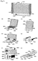
- Figs. 5(A) to 5(G) show specific examples of these electronic devices.
- Fig. 5(A) is a display device, which includes a frame body 5101, a support 5102, a display portion 5103, a speaker portion 5104, a video input terminal 5105, and the like.
- a light-emitting device that has an electroluminescent device according to the present invention is used for the display portion 2003.
- the display device includes all devices for displaying information such as for a personal computer, for receiving TV broad casting, and for displaying an advertisement.
- Fig. 5(B) is a laptop personal computer, which includes a main body 5201, a frame body 5202, a display portion 5203, a keyboard 5204, an external connection port 5205, a pointing mouse 5206, and the like.
- a light-emitting device that has an electroluminescent device according to the present invention is used for the display portion 5203.
- Fig. 5(C) is a mobile computer, which includes a main body 5301, a display portion 5302, a switch 5303, an operation key 5304, an infrared port 5305, and the like.
- a light-emitting device that has an electroluminescent device according to the present invention is used for the display portion 5302.
- Fig. 5(D) is a portable image reproduction device equipped with a recording medium (specifically, a DVD reproduction device), which includes a main body 5401, a frame body 5402, a display portion A 5403, a display portion B 5404, a recording medium (such as DVD) reading portion 5405, an operation key 5406, a speaker portion 5407, and the like.
- the display portion A 5403 is used mainly for displaying image information while the display portion B 5404 is used mainly for displaying character information, and a light-emitting device that has an electroluminescent device according to the present invention is used for these display portion A 5403 and display portion B 5404.
- the image reproduction device equipped with the recording medium further includes a home game machine and the like.
- Fig. 5(E) is a goggle-type display (head mount display), which includes a main body 5501, a display portion 5502, an arm portion 5503, and the like.
- a light-emitting device that has an electroluminescent device according to the present invention is used for the display portion 5502.
- Fig. 5(F) is a video camera, which includes a main body 5601, a display portion 5602, a frame body 5603, an external connection port 5604, a remote control receiving portion 5605, an image receiving portion 5606, a battery 5607, a sound input portion 5608, an operation key 5609, an eye piece 5610, and the like.
- a light-emitting device that has an electroluminescent device according to the present invention is used for the display portion 5602.
- Fig. 5(G) is a mobile phone, which includes a main body 5701, a frame body 5702, a display portion 5703, a voice input portion 5704, a voice output portion 5705, an operation key 5706, an external connection port 5707, an antenna 5708, and the like.
- a light-emitting device that has an electroluminescent device according to the present invention is used for the display portion 5703.
- the mobile phone can have power consumption suppressed by displaying white characters on a black background in the display portion 5703.
- a light-emitting device that has an electroluminescent device according to the present invention is quite widely applied, and is applicable to electronic devices in all fields.
Landscapes
- Chemical & Material Sciences (AREA)
- Organic Chemistry (AREA)
- Engineering & Computer Science (AREA)
- Materials Engineering (AREA)
- Electroluminescent Light Sources (AREA)
Abstract
Description








Claims (10)
- An organometallic complex represented by the following general formula 2:(where R1 is an alkyl group, an aryl group, a substituted aryl group, a heterocyclic group or a substituted heterocyclic group; R2 is hydrogen, an alkyl group, an aryl group, a substituted aryl group, a heterocyclic group, or a substituted heterocyclic group; R3, R4, R5, and R6 may be identical or different, and are individually hydrogen, halogen, an alkyl group, an alkoxyl group, an aryl group, a substituted aryl group, a heterocyclic group, or a substituted heterocyclic group; M is an element of Group 9 or an element of Group 10, and n = 2 when the M is the element of Group 9 or n = 1 when the M is the element of Group 10; and L is a monoanionic ligand having a β-diketone structure, a monoanionic bidentate ligand having a carboxyl group, or a monoanionic bidentate ligand having a phenolic hydroxyl group)

- The organometallic complex according to claim 1, wherein the M is iridium or platinum.
- The organometallic complex according to claim 1 or claim 2, wherein the L is any of monoanionic ligands shown by the following structure formulas 3 to 9.



- An electroluminescent device using the organometallic complex according to claim 1.
- An electroluminescent device using the organometallic complex according to claim 2.
- An electroluminescent device using the organometallic complex according to claim 3.
- An electroluminescent device using the organometallic complex according to claim 1 as a light emitter.
- An electroluminescent device using the organometallic complex according to claim 2 as a light emitter.
- An electroluminescent device using the organometallic complex according to claim 3 as a light emitter.
- A light-emitting device using the electroluminescent device according to any of claims 4 to 9.
Applications Claiming Priority (3)
| Application Number | Priority Date | Filing Date | Title |
|---|---|---|---|
| JP2002368990 | 2002-12-19 | ||
| JP2002368990 | 2002-12-19 | ||
| PCT/JP2003/015765 WO2004056839A1 (en) | 2002-12-19 | 2003-12-10 | Organometal complex, electroluminescent element containing the organometal complex and luminescent device including the electroluminescent element |
Publications (2)
| Publication Number | Publication Date |
|---|---|
| EP1574514A1 true EP1574514A1 (en) | 2005-09-14 |
| EP1574514A4 EP1574514A4 (en) | 2009-11-11 |
Family
ID=32677132
Family Applications (1)
| Application Number | Title | Priority Date | Filing Date |
|---|---|---|---|
| EP03778761A Withdrawn EP1574514A4 (en) | 2002-12-19 | 2003-12-10 | Organometal complex, electroluminescent element containing the organometal complex and luminescent device including the electroluminescent element |
Country Status (7)
| Country | Link |
|---|---|
| US (1) | US7413816B2 (en) |
| EP (1) | EP1574514A4 (en) |
| JP (1) | JP4683924B2 (en) |
| KR (1) | KR101033796B1 (en) |
| CN (1) | CN1729198B (en) |
| AU (1) | AU2003289000A1 (en) |
| WO (1) | WO2004056839A1 (en) |
Cited By (5)
| Publication number | Priority date | Publication date | Assignee | Title |
|---|---|---|---|---|
| US7771844B2 (en) | 2004-12-03 | 2010-08-10 | Semiconductor Energy Laboratory Co., Ltd | Organic metal complex and photoelectronic device, light-emitting element and light-emitting device using the same |
| US7795429B2 (en) | 2004-12-03 | 2010-09-14 | Semiconductor Energy Laboratory Co., Ltd. | Organometallic complex, and light-emitting element and light-emitting device using the organometallic complex |
| US7811677B2 (en) | 2004-05-20 | 2010-10-12 | Semiconductor Energy Laboratory Co., Ltd. | Light emitting element and light emitting device |
| US7915409B2 (en) | 2003-12-02 | 2011-03-29 | Semiconductor Energy Laboratory Co., Ltd. | Organometal complex and light-emitting element using the same |
| US7951471B2 (en) | 2004-12-07 | 2011-05-31 | Semiconductor Energy Laboratory Co., Ltd. | Organometallic complex, and light-emitting element and light-emitting device using the same |
Families Citing this family (12)
| Publication number | Priority date | Publication date | Assignee | Title |
|---|---|---|---|---|
| US6998492B2 (en) * | 2003-05-16 | 2006-02-14 | Semiconductor Energy Laboratory Co., Ltd. | Organometallic complex and light-emitting element containing the same |
| DE102004035965B4 (en) * | 2004-07-23 | 2007-07-26 | Novaled Ag | Top-emitting, electroluminescent component with at least one organic layer |
| WO2006104177A1 (en) * | 2005-03-28 | 2006-10-05 | Semiconductor Energy Laboratory Co., Ltd. | Organometallic complex, and light-emitting device and electronic appliance using the same |
| EP1911079A4 (en) | 2005-07-25 | 2012-05-09 | Semiconductor Energy Lab | Light-emitting element, light-emitting device, and electronic appliance |
| DE102005039064A1 (en) * | 2005-08-18 | 2007-03-01 | Merck Patent Gmbh | metal complexes |
| DE102005043165A1 (en) | 2005-09-12 | 2007-03-22 | Merck Patent Gmbh | metal complexes |
| KR100707608B1 (en) * | 2005-10-21 | 2007-04-13 | 삼성에스디아이 주식회사 | Organic light emitting display |
| JP2007269735A (en) | 2006-03-31 | 2007-10-18 | Canon Inc | Metal complex, light emitting element and display device |
| US8476822B2 (en) * | 2007-11-09 | 2013-07-02 | Universal Display Corporation | Saturated color organic light emitting devices |
| DE102008057051B4 (en) * | 2008-11-13 | 2021-06-17 | Merck Patent Gmbh | Materials for organic electroluminescent devices |
| WO2014199842A1 (en) | 2013-06-14 | 2014-12-18 | Semiconductor Energy Laboratory Co., Ltd. | Organometallic iridium complex, light-emitting element, light-emitting device, and lighting device |
| KR102696803B1 (en) | 2016-12-13 | 2024-08-21 | 삼성디스플레이 주식회사 | Compound and Organic light emitting device comprising same |
Family Cites Families (30)
| Publication number | Priority date | Publication date | Assignee | Title |
|---|---|---|---|---|
| EP0723701B1 (en) | 1994-08-11 | 2000-01-12 | Koninklijke Philips Electronics N.V. | Solid-state image intensifier and x-ray examination apparatus comprising a solid-state image intensifier |
| US6830828B2 (en) * | 1998-09-14 | 2004-12-14 | The Trustees Of Princeton University | Organometallic complexes as phosphorescent emitters in organic LEDs |
| JP4505067B2 (en) * | 1998-12-16 | 2010-07-14 | 淳二 城戸 | Organic electroluminescent device |
| GB9901971D0 (en) * | 1999-02-01 | 1999-03-17 | South Bank Univ Entpr Ltd | Electroluminescent material |
| KR101166264B1 (en) * | 1999-03-23 | 2012-07-17 | 유니버시티 오브 서던 캘리포니아 | Cyclometallated metal complexes as phosphorescent dopants in organic leds |
| KR100373203B1 (en) * | 1999-03-31 | 2003-02-25 | 주식회사 엘지화학 | New organometallic complexes for use in light emitting devices |
| US6310360B1 (en) | 1999-07-21 | 2001-10-30 | The Trustees Of Princeton University | Intersystem crossing agents for efficient utilization of excitons in organic light emitting devices |
| CA2397644A1 (en) | 2000-01-18 | 2001-07-26 | The Regents Of The University Of California | Acid addition salts of imidazolidinones as reaction catalysts |
| TW536836B (en) * | 2000-05-22 | 2003-06-11 | Semiconductor Energy Lab | Light emitting device and electrical appliance |
| US7339317B2 (en) | 2000-06-05 | 2008-03-04 | Semiconductor Energy Laboratory Co., Ltd. | Light-emitting device having triplet and singlet compound in light-emitting layers |
| US6864628B2 (en) | 2000-08-28 | 2005-03-08 | Semiconductor Energy Laboratory Co., Ltd. | Light emitting device comprising light-emitting layer having triplet compound and light-emitting layer having singlet compound |
| AU2002222565A1 (en) * | 2000-11-30 | 2002-06-11 | Canon Kabushiki Kaisha | Luminescent element and display |
| EP1217668A1 (en) | 2000-12-22 | 2002-06-26 | Covion Organic Semiconductors GmbH | Use of boron and aluminium compounds in electronic devices |
| JP2002246172A (en) * | 2001-02-14 | 2002-08-30 | Fuji Photo Film Co Ltd | Light-emitting element and manufacturing method for the same |
| GB0104700D0 (en) | 2001-02-26 | 2001-04-11 | Isis Innovation | Luminescent polymers |
| WO2002071813A1 (en) | 2001-03-02 | 2002-09-12 | The Trustees Of Princeton University | Double doped-layer, phosphorescent organic light emitting devices |
| US6787249B2 (en) | 2001-03-28 | 2004-09-07 | Semiconductor Energy Laboratory Co., Ltd. | Organic light emitting element and light emitting device using the same |
| US7504161B2 (en) | 2001-03-30 | 2009-03-17 | Fujifilm Corporation | Luminescent element |
| CN100582195C (en) | 2001-04-13 | 2010-01-20 | 株式会社半导体能源研究所 | Organic light-emitting element and light-emitting device using the same |
| DE10150477A1 (en) * | 2001-10-16 | 2003-04-17 | Bayer Ag | Layer arrangement useful in electroluminescent devices has electrically conductive layers coated with a conductive organic polymer system |
| JP3605083B2 (en) * | 2002-02-27 | 2004-12-22 | 三洋電機株式会社 | Light emitting material for light emitting device and organic electroluminescent device |
| AU2003260959A1 (en) | 2002-09-11 | 2004-04-30 | Semiconductor Energy Laboratory Co., Ltd. | Light-emitting apparatus and fabrication method of the same |
| WO2004048395A1 (en) | 2002-11-26 | 2004-06-10 | Semiconductor Energy Laboratory Co., Ltd. | Phosphorescent compound and electroluminescent element including the same |
| US7063900B2 (en) | 2002-12-23 | 2006-06-20 | General Electric Company | White light-emitting organic electroluminescent devices |
| TWI267545B (en) | 2003-06-17 | 2006-12-01 | Univ Tsinghua | Electroluminescent conjugated polymers containing phosphorescent moieties and the application thereof in LED |
| US7118812B2 (en) | 2003-12-05 | 2006-10-10 | Eastman Kodak Company | Organic element for electroluminescent devices |
| US6824895B1 (en) | 2003-12-05 | 2004-11-30 | Eastman Kodak Company | Electroluminescent device containing organometallic compound with tridentate ligand |
| US7147937B2 (en) | 2003-12-05 | 2006-12-12 | Eastman Kodak Company | Organic element for electroluminescent devices |
| US7090930B2 (en) | 2003-12-05 | 2006-08-15 | Eastman Kodak Company | Organic element for electroluminescent devices |
| US7029766B2 (en) | 2003-12-05 | 2006-04-18 | Eastman Kodak Company | Organic element for electroluminescent devices |
-
2003
- 2003-12-10 EP EP03778761A patent/EP1574514A4/en not_active Withdrawn
- 2003-12-10 KR KR1020057011408A patent/KR101033796B1/en not_active Expired - Fee Related
- 2003-12-10 WO PCT/JP2003/015765 patent/WO2004056839A1/en not_active Ceased
- 2003-12-10 JP JP2004536356A patent/JP4683924B2/en not_active Expired - Fee Related
- 2003-12-10 CN CN2003801071216A patent/CN1729198B/en not_active Expired - Fee Related
- 2003-12-10 AU AU2003289000A patent/AU2003289000A1/en not_active Abandoned
- 2003-12-17 US US10/736,679 patent/US7413816B2/en not_active Expired - Lifetime
Non-Patent Citations (2)
| Title |
|---|
| No further relevant documents disclosed * |
| See also references of WO2004056839A1 * |
Cited By (11)
| Publication number | Priority date | Publication date | Assignee | Title |
|---|---|---|---|---|
| US7915409B2 (en) | 2003-12-02 | 2011-03-29 | Semiconductor Energy Laboratory Co., Ltd. | Organometal complex and light-emitting element using the same |
| US8278444B2 (en) | 2003-12-02 | 2012-10-02 | Semiconductor Energy Laboratory Co., Ltd. | Organometal complex and light-emitting element using the same |
| US8569486B2 (en) | 2003-12-02 | 2013-10-29 | Semiconductor Energy Laboratory Co., Ltd. | Organometal complex and light-emitting element using the same |
| US9219236B2 (en) | 2003-12-02 | 2015-12-22 | Semiconductor Energy Laboratory Co., Ltd. | Organometal complex and light-emitting element using the same |
| US7811677B2 (en) | 2004-05-20 | 2010-10-12 | Semiconductor Energy Laboratory Co., Ltd. | Light emitting element and light emitting device |
| US8637167B2 (en) | 2004-05-20 | 2014-01-28 | Semiconductor Energy Laboratory Co., Ltd. | Light emitting element and light emitting device |
| US7771844B2 (en) | 2004-12-03 | 2010-08-10 | Semiconductor Energy Laboratory Co., Ltd | Organic metal complex and photoelectronic device, light-emitting element and light-emitting device using the same |
| US7795429B2 (en) | 2004-12-03 | 2010-09-14 | Semiconductor Energy Laboratory Co., Ltd. | Organometallic complex, and light-emitting element and light-emitting device using the organometallic complex |
| US8512880B2 (en) | 2004-12-03 | 2013-08-20 | Semiconductor Energy Laboratory Co., Ltd. | Organometallic complex, and light-emitting element and light-emitting device using the organometallic complex |
| US7951471B2 (en) | 2004-12-07 | 2011-05-31 | Semiconductor Energy Laboratory Co., Ltd. | Organometallic complex, and light-emitting element and light-emitting device using the same |
| US8227600B2 (en) | 2004-12-07 | 2012-07-24 | Semiconductor Energy Laboratory Co., Ltd. | Organometallic complex, and light-emitting element and light-emitting device using the same |
Also Published As
| Publication number | Publication date |
|---|---|
| US7413816B2 (en) | 2008-08-19 |
| CN1729198B (en) | 2010-11-03 |
| JPWO2004056839A1 (en) | 2006-04-20 |
| KR20050084419A (en) | 2005-08-26 |
| CN1729198A (en) | 2006-02-01 |
| KR101033796B1 (en) | 2011-05-13 |
| WO2004056839A1 (en) | 2004-07-08 |
| EP1574514A4 (en) | 2009-11-11 |
| AU2003289000A1 (en) | 2004-07-14 |
| US20040241493A1 (en) | 2004-12-02 |
| JP4683924B2 (en) | 2011-05-18 |
Similar Documents
| Publication | Publication Date | Title |
|---|---|---|
| US8278444B2 (en) | Organometal complex and light-emitting element using the same | |
| US7078114B2 (en) | Phosphorescence compound and electro field light emitting device having the same | |
| US7413816B2 (en) | Organic metallic complex and electroluminescent element using the same | |
| KR101054663B1 (en) | Organometallic complexes, electroluminescent materials using these complexes, and electroluminescent devices using these complexes | |
| CN101151270A (en) | Organometallic complex, and light-emitting device and electronic device using the same | |
| JP4312678B2 (en) | Organometallic complex, and light emitting device and electronic device using the same | |
| JP4080518B2 (en) | Electroluminescent device, light emitting device, and electric appliance |
Legal Events
| Date | Code | Title | Description |
|---|---|---|---|
| PUAI | Public reference made under article 153(3) epc to a published international application that has entered the european phase |
Free format text: ORIGINAL CODE: 0009012 |
|
| 17P | Request for examination filed |
Effective date: 20050615 |
|
| AK | Designated contracting states |
Kind code of ref document: A1 Designated state(s): AT BE BG CH CY CZ DE DK EE ES FI FR GB GR HU IE IT LI LU MC NL PT RO SE SI SK TR |
|
| AX | Request for extension of the european patent |
Extension state: AL LT LV MK |
|
| DAX | Request for extension of the european patent (deleted) | ||
| RBV | Designated contracting states (corrected) |
Designated state(s): DE FI FR GB NL |
|
| A4 | Supplementary search report drawn up and despatched |
Effective date: 20091013 |
|
| 17Q | First examination report despatched |
Effective date: 20100726 |
|
| GRAP | Despatch of communication of intention to grant a patent |
Free format text: ORIGINAL CODE: EPIDOSNIGR1 |
|
| RIC1 | Information provided on ipc code assigned before grant |
Ipc: C07F 15/00 20060101AFI20170706BHEP Ipc: C09K 11/06 20060101ALI20170706BHEP Ipc: C07C 251/24 20060101ALI20170706BHEP |
|
| INTG | Intention to grant announced |
Effective date: 20170803 |
|
| STAA | Information on the status of an ep patent application or granted ep patent |
Free format text: STATUS: THE APPLICATION IS DEEMED TO BE WITHDRAWN |
|
| 18D | Application deemed to be withdrawn |
Effective date: 20171214 |
|
| RIC1 | Information provided on ipc code assigned before grant |
Ipc: C07C 251/24 20060101ALI20170706BHEP Ipc: C07F 15/00 20060101AFI20170706BHEP Ipc: C09K 11/06 20060101ALI20170706BHEP |