EP1569014A1 - Optical retardation plate and method of manufacturing the same - Google Patents
Optical retardation plate and method of manufacturing the same Download PDFInfo
- Publication number
- EP1569014A1 EP1569014A1 EP05251146A EP05251146A EP1569014A1 EP 1569014 A1 EP1569014 A1 EP 1569014A1 EP 05251146 A EP05251146 A EP 05251146A EP 05251146 A EP05251146 A EP 05251146A EP 1569014 A1 EP1569014 A1 EP 1569014A1
- Authority
- EP
- European Patent Office
- Prior art keywords
- optical retardation
- retardation plate
- dielectric medium
- amorphous dielectric
- grating pattern
- Prior art date
- Legal status (The legal status is an assumption and is not a legal conclusion. Google has not performed a legal analysis and makes no representation as to the accuracy of the status listed.)
- Granted
Links
- 230000003287 optical effect Effects 0.000 title claims abstract description 57
- 238000004519 manufacturing process Methods 0.000 title claims description 17
- 238000000034 method Methods 0.000 claims abstract description 48
- 239000000758 substrate Substances 0.000 claims abstract description 43
- 238000007669 thermal treatment Methods 0.000 claims abstract description 43
- 238000005530 etching Methods 0.000 claims abstract description 32
- 230000001788 irregular Effects 0.000 claims abstract description 15
- 230000000737 periodic effect Effects 0.000 claims abstract description 7
- 239000013081 microcrystal Substances 0.000 claims abstract description 5
- GWEVSGVZZGPLCZ-UHFFFAOYSA-N Titan oxide Chemical compound O=[Ti]=O GWEVSGVZZGPLCZ-UHFFFAOYSA-N 0.000 claims description 6
- 238000010438 heat treatment Methods 0.000 claims description 4
- 239000010955 niobium Substances 0.000 claims description 3
- 229910052758 niobium Inorganic materials 0.000 claims description 2
- GUCVJGMIXFAOAE-UHFFFAOYSA-N niobium atom Chemical compound [Nb] GUCVJGMIXFAOAE-UHFFFAOYSA-N 0.000 claims description 2
- 229910052710 silicon Inorganic materials 0.000 claims description 2
- 239000010703 silicon Substances 0.000 claims description 2
- 239000004408 titanium dioxide Substances 0.000 claims description 2
- 230000004907 flux Effects 0.000 claims 2
- 239000002245 particle Substances 0.000 description 13
- 229920002120 photoresistant polymer Polymers 0.000 description 9
- 239000011651 chromium Substances 0.000 description 6
- VYZAMTAEIAYCRO-UHFFFAOYSA-N Chromium Chemical compound [Cr] VYZAMTAEIAYCRO-UHFFFAOYSA-N 0.000 description 5
- 229910052804 chromium Inorganic materials 0.000 description 5
- 238000012937 correction Methods 0.000 description 3
- 239000013078 crystal Substances 0.000 description 3
- 238000002474 experimental method Methods 0.000 description 3
- 239000010453 quartz Substances 0.000 description 3
- VYPSYNLAJGMNEJ-UHFFFAOYSA-N silicon dioxide Inorganic materials O=[Si]=O VYPSYNLAJGMNEJ-UHFFFAOYSA-N 0.000 description 3
- 230000015572 biosynthetic process Effects 0.000 description 2
- 238000005498 polishing Methods 0.000 description 2
- XUIMIQQOPSSXEZ-UHFFFAOYSA-N Silicon Chemical compound [Si] XUIMIQQOPSSXEZ-UHFFFAOYSA-N 0.000 description 1
- 239000006096 absorbing agent Substances 0.000 description 1
- 230000007423 decrease Effects 0.000 description 1
- 238000001746 injection moulding Methods 0.000 description 1
- 150000002500 ions Chemical class 0.000 description 1
- 239000000463 material Substances 0.000 description 1
- 230000007935 neutral effect Effects 0.000 description 1
- 238000000016 photochemical curing Methods 0.000 description 1
- 238000000206 photolithography Methods 0.000 description 1
- 238000001020 plasma etching Methods 0.000 description 1
- 238000012545 processing Methods 0.000 description 1
- 229920005989 resin Polymers 0.000 description 1
- 239000011347 resin Substances 0.000 description 1
- 238000000992 sputter etching Methods 0.000 description 1
- 229920005992 thermoplastic resin Polymers 0.000 description 1
- 238000012546 transfer Methods 0.000 description 1
Images




Classifications
-
- G—PHYSICS
- G02—OPTICS
- G02B—OPTICAL ELEMENTS, SYSTEMS OR APPARATUS
- G02B5/00—Optical elements other than lenses
- G02B5/18—Diffraction gratings
- G02B5/1847—Manufacturing methods
- G02B5/1857—Manufacturing methods using exposure or etching means, e.g. holography, photolithography, exposure to electron or ion beams
-
- G—PHYSICS
- G02—OPTICS
- G02B—OPTICAL ELEMENTS, SYSTEMS OR APPARATUS
- G02B5/00—Optical elements other than lenses
- G02B5/30—Polarising elements
- G02B5/3083—Birefringent or phase retarding elements
-
- Y—GENERAL TAGGING OF NEW TECHNOLOGICAL DEVELOPMENTS; GENERAL TAGGING OF CROSS-SECTIONAL TECHNOLOGIES SPANNING OVER SEVERAL SECTIONS OF THE IPC; TECHNICAL SUBJECTS COVERED BY FORMER USPC CROSS-REFERENCE ART COLLECTIONS [XRACs] AND DIGESTS
- Y10—TECHNICAL SUBJECTS COVERED BY FORMER USPC
- Y10T—TECHNICAL SUBJECTS COVERED BY FORMER US CLASSIFICATION
- Y10T428/00—Stock material or miscellaneous articles
- Y10T428/24—Structurally defined web or sheet [e.g., overall dimension, etc.]
- Y10T428/24479—Structurally defined web or sheet [e.g., overall dimension, etc.] including variation in thickness
- Y10T428/24612—Composite web or sheet
-
- Y—GENERAL TAGGING OF NEW TECHNOLOGICAL DEVELOPMENTS; GENERAL TAGGING OF CROSS-SECTIONAL TECHNOLOGIES SPANNING OVER SEVERAL SECTIONS OF THE IPC; TECHNICAL SUBJECTS COVERED BY FORMER USPC CROSS-REFERENCE ART COLLECTIONS [XRACs] AND DIGESTS
- Y10—TECHNICAL SUBJECTS COVERED BY FORMER USPC
- Y10T—TECHNICAL SUBJECTS COVERED BY FORMER US CLASSIFICATION
- Y10T428/00—Stock material or miscellaneous articles
- Y10T428/24—Structurally defined web or sheet [e.g., overall dimension, etc.]
- Y10T428/24802—Discontinuous or differential coating, impregnation or bond [e.g., artwork, printing, retouched photograph, etc.]
Definitions
- the present invention relates to an optical retardation plate using a dielectric medium, and a method of manufacturing the same.
- an optical retardation plate has been manufactured by polishing a crystalline plate made of a quartz crystal.
- a thickness of the optical retardation plate is adjusted so that a phase retardation between ordinary light and extraordinary light becomes an (N + 1/4) wavelength (N: integral number) in a 1/4 retardation plate, an (N + 1/2) wavelength in a 1/2 retardation plate, and an N wavelength in a full retardation plate.
- the optical retardation plate using a grating utilizes a fact that a refractive index na in a direction parallel to an extension direction of trenches of the grating and a refractive index nb in a direction intersecting perpendicularly the extension direction of the trenches of the grating are different from each other in an area where a wavelength ⁇ is sufficiently smaller than a pitch d.
- na ⁇ n 1 2 + n 2 2 (1 - q) ⁇ 1/2
- nb ⁇ (1/n 1 ) 2 q + (1/n 2 ) 2 (1 - q) ⁇ -1/2
- n 1 is a refractive index of a first medium
- n 2 is a refractive index of a second medium
- q is a ratio which the first medium occupies for one period of the grating and which is in.a range of 0 ⁇ q ⁇ 1.
- Equation (4) it is understood from Equation (4) that in order to obtain a large phase retardation ⁇ , the depth D of each trench has to be increased or the magnitude ⁇ n of the double refraction has to be increased. This relationship is established not only when the grating shape is rectangular, but also when the grating shape is a sine wave-like shape, a chopping wave-like shape, or the like.
- a first method is a method in which a grating is formed in a photoresist film by utilizing an interference exposure method, a mold is manufactured from the resultant grating, and the grating is transferred to a thermoplastic resin through the mold by utilizing a hot press method or an injection molding method, or is transferred to a photocuring resin.
- a second method is a method in which a grating made of a photoresist film is formed on a dielectric substrate similarly to the first method, and the dielectric substrate is selectively etched away by utilizing an ion etching method or a reactive ion etching method using the photoresist film as an etching mask to obtain a grating on a surface of the dielectric substrate.
- a grating formed on a photoresist film is transferred to a material having high etching resistance, e.g., a chromium (Cr) film, and etching is carried out using the chromium film as an etching mask, progress of the etching is blocked since along with an increase in depth of each trench of the grating, a dielectric medium which is etched once is restucked to a surface of a substrate, and the number of particles such as active radicals, ions or neutral particles which arrive at bottom portions of trenches decreases.
- it is difficult to form a grating having a desired shape.
- Such a problem arises irrespective of a shape of a grating.
- a size of a substrate is large, uniformity within a surface during the etching becomes poor, and hence an excellent manufacture yield cannot be obtained.
- JP 7-99402 B discloses that a grating is covered with a dielectric medium having a sufficiently large refractive index to make a depth of each trench small in order to cope with those problems.
- the dielectric medium is difficult to be formed to a bottom portion of each trench since a width of each trench is small.
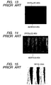
- Fig. 13 shows a conventional manufacture example in a general film formation state in which no film management is carried out, i.e., Fig. 13 shows a cross section image, observed with a scanning electron microscope (SEM), of a formed film which is obtained by mixedly forming an amorphous film and a crystallized film each made of titanium dioxide (TiO 2 ) on a quartz wafer.
- SEM scanning electron microscope
- an upper portion having a columnar structure is a crystallized area and a lower portion is an amorphous area.
- Fig. 14 shows a cross section image, observed with a SEM, of a grating which is formed by selectively etching away the dielectric medium. It is generally known that a crystallized area and an amorphous area are different in etching rate, and the etching rate of the amorphous area is higher than that of the crystallized area. From this fact, the cross section image of Fig. 14 shows that since side etch for a lower area especially progresses, this lower area is the amorphous area.
- the phase retardation ⁇ which the light made incident to the grating undergoes is proportional to the depth D of each trench of the grating and the magnitude ⁇ n of the double refraction. Then, a dielectric medium which is much larger in refractive index than a dielectric substrate is formed on the dielectric substrate to form a grating shape, thereby allowing the depth D of each trench of the grating to be made small.
- the etching rate differs depending on lattice directions of a crystal, or the amorphous area and the crystallized area are different in etching rate. Accordingly, uniform etching becomes difficult to carry out.
- the present invention has been made in order to address the above-mentioned problems, and it is, therefore, an object of the present invention to provide a phase grating type optical retardation plate for which a dielectric medium in an amorphous state is formed on a dielectric substrate, thereby making uniform etching possible, and a method of manufacturing the same.
- an optical retardation plate is manufactured by utilizing a method including: forming at least one kind of amorphous dielectric medium on a substrate; and etching the at least one kind of amorphous dielectric medium to form an irregular grating pattern having a periodic structure having a period equal to or shorter than a wavelength in use.
- a method of manufacturing an optical retardation plate includes: forming at least one kind of amorphous dielectric medium on a substrate; etching the at least one kind of amorphous dielectric medium to form an irregular grating pattern having a periodic structure with a period equal to or shorter than a wavelength in use; and crystallizing the etched dielectric medium through a thermal treatment to increase a refractive index of the film and to increase a phase retardation in the irregular grating pattern.
- the etching processing is executed using the film which is obtained by forming the dielectric medium while the dielectric medium is maintained in the amorphous state, whereby a product having a nearly rectangle grating shape and having no etching nonuniformity within the grating can be inexpensively mass-produced in high yields.
- performing thermal treatment makes it possible to increase the phase retardation in the irregular grating pattern.
- Fig. 1 is a cross sectional view showing a state in which a surface of a dielectric substrate 1 having a refractive index n 1 is coated with an amorphous dielectric medium 2 having a refractive index n 2 larger than the refractive index n 1 , and the amorphous dielectric medium 2 is selectively etched away to form a rectangular grating 3. Then, when the refractive index n 2 of the amorphous dielectric medium 2 increases through a thermal treatment, a magnitude ⁇ n of structure double refraction increases accordingly. Thus, the magnitude ⁇ n of the structure double refraction is made large without making a depth D of each trench of the rectangular grating 3 large in accordance with Equation (4), thereby increasing a phase retardation ⁇ .
- Fig. 2 is a process flow chart for Embodiment 1 of the present invention.
- the amorphous dielectric medium 2 made of titanium dioxide (TiO 2 ) in an amorphous state is formed on the surface of the dielectric substrate 1 made of a quartz wafer, and a chromium film and a photoresist film are sequentially formed on the amorphous dielectric medium 2.
- the photoresist film is patterned through a photolithography process.
- the chromium film is selectively etched away using the patterned photoresist film as an etching mask, and the amorphous dielectric medium 2 is selectively etched away using the patterned chromium film as an etching mask, thereby forming the rectangular grating 3 having a periodic structure with a period shorter than a wavelength of visible light, e.g., 260 nm.
- niobium (Nb) and silicon (Si) may be added to the titanium dioxide film as the amorphous dielectric medium 2 to adjust the refractive index n 2 of the amorphous dielectric medium 2.
- Fig. 3 is a cross section image, observed with a SEM, of the rectangular grating 3. It can be seen from Fig. 3 that the amorphous dielectric medium 2 and the rectangular grating 3 are formed on the dielectric substrate 1, and the optical retardation plate using an irregular grating pattern having the rectangular grating 3 is ideally manufactured.
- Fig. 4 is a process flow chart for a Second Embodiment.
- a thermal treatment is further carried out for the optical retardation plate manufactured in accordance with the method described in the First Embodiment at 700°C or 800°C for one hour to form microcrystal particles in the amorphous dielectric medium 2.
- the refractive index n 2 of the amorphous medium 2 is -increased to increase phase retardation in terms of phase retardation characteristics.
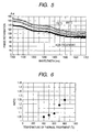
- Fig. 5 is a graphical representation in which data on the phase retardations measured after completion of the above-mentioned thermal treatment is plotted against data on wavelengths.
- the graph shows that the thermal treatment at 700°C or 800°C for one hour makes the phase retardation ⁇ in the optical retardation plate of the Second Embodiment larger than that in the optical retardation plate of the First Embodiment which is manufactured without carrying out the thermal treatment; and as the temperature during the thermal treatment becomes higher, a ratio in amount of the microcrystalline particles to the amorphous dielectric medium 2 further increases, and hence the phase retardation ⁇ becomes larger.
- the additional thermal treatment makes the refractive index n 2 of the amorphous dielectric medium 2 large to increase a difference in refractive index between the amorphous dielectric medium 2 and a surrounding medium such as air, thereby increasing the magnitude ⁇ n of the double refraction. Therefore, the phase retardation ⁇ in the optical retardation plate of the Second Embodiment can be made larger than that in the optical retardation plate manufactured in accordance with the method described in the First Embodiment.
- Fig. 6 shows a graphical representation which is obtained such that the thermal treatments are carried out for the optical retardation plates each having the amorphous dielectric medium 2 formed under the same conditions at 400°C, 500°C, 600°C, 700°C and 800°C, respectively, in accordance with the method described in the Second Embodiment, and ratios of the phase retardations ⁇ after completion of the respective thermal treatments are plotted against the respective thermal treatment temperatures when the phase retardation ⁇ before any of the thermal treatments is normalized as 1. It is understood from Fig. 6 as well that the phase retardation ⁇ after the thermal treatment further increases as the temperature of the thermal treatment is higher.
- the additional thermal treatment is applied to the irregular grating pattern having the rectangular grating 3 in the amorphous dielectric medium 2 in such a manner, whereby the desired phase retardation ⁇ can be obtained even when a depth of each trench of the rectangular grating 3 of the amorphous dielectric medium 2 is made small through the etching process.
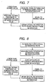
- Fig. 7 shows a process flow chart for a Third Embodiment.
- phase retardation ⁇ of the optical retardation plate immediately after its manufacture in accordance with the method described in the First Embodiment is 150° but the desired phase retardation ⁇ of the optical retardation plate is 180° for example, it is necessary to correct a shortage of 30°.
- the thermal treatment corresponding to the correction for the shortage of 30° may be carried out using this relationship.
- thermal treatment at 700°C corresponds to the correction for the shortage of 30°
- thermal treatment at 700°C is carried out for the optical retardation plate to crystallize the amorphous dielectric medium 2 or generate a large number of microcrystalline particles, thereby correcting the phase retardation ⁇ .
- the optical retardation plate having the target phase retardation ⁇ of 180°C.
- Fig. 8 is a process flow chart for a Fourth Embodiment.
- the optical retardation plates each having the normal rectangular grating 3 are manufactured, the optical retardation plates are manufactured by collectively, selectively etching away the dielectric substrate 1.
- the depths of the trenches of the rectangular gratings 3 within the surface of the dielectric substrate 1 may not be uniform due to nonuniformity in an internal state of an etching system, and hence the phase retardations ⁇ within the surface of the dielectric substrate 1 may not be uniform in some cases.
- the dielectric substrate 1 is cut to separate the optical retardation plates from one another, and the optical retardation plates having near phase retardations ⁇ are then collected. Then, the thermal treatment is carried out for the collected optical retardation plates in accordance with the method described in Embodiment 3, thereby correcting the near phase retardations ⁇ .
- the thermal treatments can be carried out at respective temperatures suitable for the optical retardation plates when the uniformity of the depths of the rectangular gratings 3 within the dielectric substrate 1 is poor, all the irregular grating patterns within the dielectric substrate 1 can be corrected so as for each of them to have the desired phase retardation ⁇ .
- the phase retardations within the surface of the dielectric substrate 1 are not uniform.
- the optical retardation plates may show a tendency in which the depth of the trench of the rectangular grating 3 is shallow at a central portion of the dielectric substrate 1 while the depth of the trench of the rectangular grating 3 becomes deep in a position located more outward, concentrically within the dielectric substrate 1, or the depth of the trench of the rectangular grating 3 is deep at the central portion of the dielectric substrate 1, while the depth of the trench of the rectangular grating 3 becomes shallow in a position located more outward, concentrically within the dielectric substrate 1 in some cases.
- the phase retardation ⁇ within the surface of the dielectric substrate 1 also changes concentrically.
- a heat source 12 of a thermal treatment system 11 is installed so as to be located at a center of the dielectric substrate 1, and the thermal treatment is carried out so that a temperature further drops in a position located more outward, concentrically within the dielectric substrate 1.
- the heat source 12 is installed annularly outside the dielectric substrate 1, and a thermal treatment is carried out so that a temperature further drops in a position nearer the center of a concentric circle.
- the thermal treatment having a heat distribution corresponding to the concentric change of the depths is carried out, whereby all the irregular grating patterns within the dielectric substrate 1 can be corrected so that each of them have the averaged desired phase retardation ⁇ .
- Fig. 11 shows a process flow chart
- Fig. 12 is a schematic perspective view explaining the process flow shown in Fig. 11.
- the thermal treatments are carried out by radiating laser beams L having energies corresponding to the phase retardations ⁇ of the optical retardation plates within the dielectric substrate 1 onto the optical retardation plates within the dielectric substrate 1 to make temperatures locally rise, whereby each of the phase retardations in the whole area of the dielectric substrate 1 is corrected to the desired phase retardation ⁇ .
- a laser beam L is used as local heating means, any other method may be utilized.
- a method may be adopted in which not only the energy of the laser beam L is adjusted, but also a heat absorber is combined therewith as long as an amount of heating can be controlled in accordance with this method.
Landscapes
- Physics & Mathematics (AREA)
- General Physics & Mathematics (AREA)
- Optics & Photonics (AREA)
- Engineering & Computer Science (AREA)
- Manufacturing & Machinery (AREA)
- Diffracting Gratings Or Hologram Optical Elements (AREA)
- Polarising Elements (AREA)
Abstract
Description
- The present invention relates to an optical retardation plate using a dielectric medium, and a method of manufacturing the same.
- Heretofore, an optical retardation plate has been manufactured by polishing a crystalline plate made of a quartz crystal. In this case, a thickness of the optical retardation plate is adjusted so that a phase retardation between ordinary light and extraordinary light becomes an (N + 1/4) wavelength (N: integral number) in a 1/4 retardation plate, an (N + 1/2) wavelength in a 1/2 retardation plate, and an N wavelength in a full retardation plate.
- In addition to such a method utilizing crystal polishing, a method using a grating utilizing structure double refraction based on a structure of dielectric is also proposed. Proposal and experiments on a retardation plate using this grating is described in an article written by D.C. Flanders: Applied Physics Letters, Vol. 42, No. 6(March 15, 1983), pp. 492 to 494.
- The optical retardation plate using a grating utilizes a fact that a refractive index na in a direction parallel to an extension direction of trenches of the grating and a refractive index nb in a direction intersecting perpendicularly the extension direction of the trenches of the grating are different from each other in an area where a wavelength λ is sufficiently smaller than a pitch d. According to the above article, when the grating has a rectangular shape, the refractive index na and the refractive index nb are given by Equations (1) and (2), respectively:
- In addition, when a depth of each trench in the grating is assigned D, a phase retardation ΔΦ which light made incident to the grating having the double refraction with the magnitude Δn undergoes is given by Equation (4):
- It is understood from Equation (4) that in order to obtain a large phase retardation ΔΦ, the depth D of each trench has to be increased or the magnitude Δn of the double refraction has to be increased. This relationship is established not only when the grating shape is rectangular, but also when the grating shape is a sine wave-like shape, a chopping wave-like shape, or the like.
- In order to concretely manufacture a retardation plate using the grating based on the above-mentioned principles, the following two methods are mainly, readily considered. A first method is a method in which a grating is formed in a photoresist film by utilizing an interference exposure method, a mold is manufactured from the resultant grating, and the grating is transferred to a thermoplastic resin through the mold by utilizing a hot press method or an injection molding method, or is transferred to a photocuring resin.
- A second method is a method in which a grating made of a photoresist film is formed on a dielectric substrate similarly to the first method, and the dielectric substrate is selectively etched away by utilizing an ion etching method or a reactive ion etching method using the photoresist film as an etching mask to obtain a grating on a surface of the dielectric substrate.
- When such a grating is manufactured by utilizing the first method, since a substantial contact surface area between a medium and an electroformed mold remarkably increases, a tensile shear force when the medium is peeled from a mold surface becomes large. For this reason, there is encountered a problem that the cured medium is peeled off from a substrate during the peeling to be left on the mold surface, and hence the transfer of the grating becomes difficult.
- In addition, in the case of the second method, since a time required for the etching extends over several hours and hence the photoresist mask able to withstand the etching is necessarily thickened, the formation of the photoresist mask is difficult.
- In addition, in a case as well where a grating formed on a photoresist film is transferred to a material having high etching resistance, e.g., a chromium (Cr) film, and etching is carried out using the chromium film as an etching mask, progress of the etching is blocked since along with an increase in depth of each trench of the grating, a dielectric medium which is etched once is restucked to a surface of a substrate, and the number of particles such as active radicals, ions or neutral particles which arrive at bottom portions of trenches decreases. Thus, it is difficult to form a grating having a desired shape. Such a problem arises irrespective of a shape of a grating. Also, when a size of a substrate is large, uniformity within a surface during the etching becomes poor, and hence an excellent manufacture yield cannot be obtained.
- JP 7-99402 B discloses that a grating is covered with a dielectric medium having a sufficiently large refractive index to make a depth of each trench small in order to cope with those problems. In case of this method as well, however, the dielectric medium is difficult to be formed to a bottom portion of each trench since a width of each trench is small.
- Fig. 13 shows a conventional manufacture example in a general film formation state in which no film management is carried out, i.e., Fig. 13 shows a cross section image, observed with a scanning electron microscope (SEM), of a formed film which is obtained by mixedly forming an amorphous film and a crystallized film each made of titanium dioxide (TiO2) on a quartz wafer. In this cross section image, an upper portion having a columnar structure is a crystallized area and a lower portion is an amorphous area.
- Fig. 14 shows a cross section image, observed with a SEM, of a grating which is formed by selectively etching away the dielectric medium. It is generally known that a crystallized area and an amorphous area are different in etching rate, and the etching rate of the amorphous area is higher than that of the crystallized area. From this fact, the cross section image of Fig. 14 shows that since side etch for a lower area especially progresses, this lower area is the amorphous area.
- When crystallized particles mixedly exist in an amorphous dielectric medium, since the etching rate of portions of the crystallized particles is low, the portions of the crystalline particles are left as shown in Fig. 15 without being etched away. In addition, the crystallized particles function as an etching mask during the etching and hence portions under the crystallized particles are not etched away. Thus, an optical retardation plate using a grating cannot be satisfactorily manufactured.
- The phase retardation ΔΦ which the light made incident to the grating undergoes, as shown in Equation (4), is proportional to the depth D of each trench of the grating and the magnitude Δn of the double refraction. Then, a dielectric medium which is much larger in refractive index than a dielectric substrate is formed on the dielectric substrate to form a grating shape, thereby allowing the depth D of each trench of the grating to be made small. However, when the dielectric medium is crystallized or the crystallized particles exist, the etching rate differs depending on lattice directions of a crystal, or the amorphous area and the crystallized area are different in etching rate. Accordingly, uniform etching becomes difficult to carry out.
- The present invention has been made in order to address the above-mentioned problems, and it is, therefore, an object of the present invention to provide a phase grating type optical retardation plate for which a dielectric medium in an amorphous state is formed on a dielectric substrate, thereby making uniform etching possible, and a method of manufacturing the same.
- In order to attain the above-mentioned object, according to one aspect of the present invention, an optical retardation plate is manufactured by utilizing a method including: forming at least one kind of amorphous dielectric medium on a substrate; and etching the at least one kind of amorphous dielectric medium to form an irregular grating pattern having a periodic structure having a period equal to or shorter than a wavelength in use.
- In addition, according to another aspect of the present invention, a method of manufacturing an optical retardation plate includes: forming at least one kind of amorphous dielectric medium on a substrate; etching the at least one kind of amorphous dielectric medium to form an irregular grating pattern having a periodic structure with a period equal to or shorter than a wavelength in use; and crystallizing the etched dielectric medium through a thermal treatment to increase a refractive index of the film and to increase a phase retardation in the irregular grating pattern.
- According to an embodiment of the method of manufacturing the optical retardation plate of the present invention, the etching processing is executed using the film which is obtained by forming the dielectric medium while the dielectric medium is maintained in the amorphous state, whereby a product having a nearly rectangle grating shape and having no etching nonuniformity within the grating can be inexpensively mass-produced in high yields.
- In addition, performing thermal treatment makes it possible to increase the phase retardation in the irregular grating pattern.
- The invention will now be described by way of example only with reference to the drawings, in which:
- Fig. 1 is a schematic cross sectional view of an optical retardation plate in which a rectangular grating is formed in a dielectric medium according to First Embodiment of the present invention;
- Fig. 2 is a process flow chart for the First Embodiment of the present invention;
- Fig. 3 is a cross section image observed with a SEM in the First Embodiment of the present invention;
- Fig. 4 is a process flow chart for a Second Embodiment of the present invention;
- Fig. 5 is a graphical representation showing a relationship between a wavelength and a phase retardation in the Second Embodiment of the present invention;
- Fig. 6 is a graphical representation showing a relationship between a temperature of a thermal treatment and a ratio in phase retardation in the Second Embodiment of the present invention;
- Fig. 7 is a process flow chart for a Third Embodiment of the present invention;
- Fig. 8 is a process flow chart for a Fourth Embodiment of the present invention;
- Fig. 9 is a plan view explaining a thermal treatment method in a Fifth Embodiment of the present invention;
- Fig. 10 is a plan view explaining another thermal treatment method in the Fifth Embodiment of the present invention;
- Fig. 11 is a process flow chart for a Sixth Embodiment of the present invention;
- Fig. 12 is a schematic perspective view explaining a thermal treatment method in the Sixth Embodiment of the present invention;
- Fig. 13 is a cross section image which is observed with a SEM and in which a crystallized film and an amorphous film mixedly exist;
- Fig. 14 is a cross section image, observed with a SEM, of a grating formed in a dielectric medium; and
- Fig. 15 is a cross section image, observed with a SEM, showing a state in which crystallized particles are left without being etched away when the crystallized particles exist in an amorphous dielectric medium.
-
- Fig. 1 is a cross sectional view showing a state in which a surface of a dielectric substrate 1 having a refractive index n1 is coated with an amorphous dielectric medium 2 having a refractive index n2 larger than the refractive index n1, and the amorphous dielectric medium 2 is selectively etched away to form a rectangular grating 3. Then, when the refractive index n2 of the amorphous dielectric medium 2 increases through a thermal treatment, a magnitude Δn of structure double refraction increases accordingly. Thus, the magnitude Δn of the structure double refraction is made large without making a depth D of each trench of the rectangular grating 3 large in accordance with Equation (4), thereby increasing a phase retardation ΔΦ.
- Fig. 2 is a process flow chart for Embodiment 1 of the present invention. The amorphous dielectric medium 2 made of titanium dioxide (TiO2) in an amorphous state is formed on the surface of the dielectric substrate 1 made of a quartz wafer, and a chromium film and a photoresist film are sequentially formed on the amorphous dielectric medium 2. The photoresist film is patterned through a photolithography process. Thereafter, the chromium film is selectively etched away using the patterned photoresist film as an etching mask, and the amorphous dielectric medium 2 is selectively etched away using the patterned chromium film as an etching mask, thereby forming the rectangular grating 3 having a periodic structure with a period shorter than a wavelength of visible light, e.g., 260 nm.
- Note that at least one of niobium (Nb) and silicon (Si) may be added to the titanium dioxide film as the amorphous dielectric medium 2 to adjust the refractive index n2 of the amorphous dielectric medium 2.
- Fig. 3 is a cross section image, observed with a SEM, of the rectangular grating 3. It can be seen from Fig. 3 that the amorphous dielectric medium 2 and the rectangular grating 3 are formed on the dielectric substrate 1, and the optical retardation plate using an irregular grating pattern having the rectangular grating 3 is ideally manufactured.
- Fig. 4 is a process flow chart for a Second Embodiment. In the Second Embodiment, a thermal treatment is further carried out for the optical retardation plate manufactured in accordance with the method described in the First Embodiment at 700°C or 800°C for one hour to form microcrystal particles in the amorphous dielectric medium 2. Thus, the refractive index n2 of the amorphous medium 2 is -increased to increase phase retardation in terms of phase retardation characteristics.
- Fig. 5 is a graphical representation in which data on the phase retardations measured after completion of the above-mentioned thermal treatment is plotted against data on wavelengths. The graph shows that the thermal treatment at 700°C or 800°C for one hour makes the phase retardation ΔΦ in the optical retardation plate of the Second Embodiment larger than that in the optical retardation plate of the First Embodiment which is manufactured without carrying out the thermal treatment; and as the temperature during the thermal treatment becomes higher, a ratio in amount of the microcrystalline particles to the amorphous dielectric medium 2 further increases, and hence the phase retardation ΔΦ becomes larger.
- It is also experimentally verified that the additional thermal treatment makes the refractive index n2 of the amorphous dielectric medium 2 large to increase a difference in refractive index between the amorphous dielectric medium 2 and a surrounding medium such as air, thereby increasing the magnitude Δn of the double refraction. Therefore, the phase retardation ΔΦ in the optical retardation plate of the Second Embodiment can be made larger than that in the optical retardation plate manufactured in accordance with the method described in the First Embodiment.
- Fig. 6 shows a graphical representation which is obtained such that the thermal treatments are carried out for the optical retardation plates each having the amorphous dielectric medium 2 formed under the same conditions at 400°C, 500°C, 600°C, 700°C and 800°C, respectively, in accordance with the method described in the Second Embodiment, and ratios of the phase retardations ΔΦ after completion of the respective thermal treatments are plotted against the respective thermal treatment temperatures when the phase retardation ΔΦ before any of the thermal treatments is normalized as 1. It is understood from Fig. 6 as well that the phase retardation ΔΦ after the thermal treatment further increases as the temperature of the thermal treatment is higher.
- The additional thermal treatment is applied to the irregular grating pattern having the rectangular grating 3 in the amorphous dielectric medium 2 in such a manner, whereby the desired phase retardation ΔΦ can be obtained even when a depth of each trench of the rectangular grating 3 of the amorphous dielectric medium 2 is made small through the etching process.
- Fig. 7 shows a process flow chart for a Third Embodiment. When the phase retardation of the optical retardation plate manufactured in accordance with the method described in the First Embodiment is smaller than the desired phase retardation ΔΦ, the thermal treatment is carried out for this optical retardation plate at a temperature permitting the desired phase retardation ΔΦ to be obtained, thereby allowing the phase retardation ΔΦ to be corrected.
- If the phase retardation ΔΦ of the optical retardation plate immediately after its manufacture in accordance with the method described in the First Embodiment is 150° but the desired phase retardation ΔΦ of the optical retardation plate is 180° for example, it is necessary to correct a shortage of 30°. When the relationship between the temperature of the thermal treatment and the retardation correction is made clear from experiments, the thermal treatment corresponding to the correction for the shortage of 30° may be carried out using this relationship.
- In the Third Embodiment, when it is verified from the experiments that thermal treatment at 700°C corresponds to the correction for the shortage of 30°, thermal treatment at 700°C is carried out for the optical retardation plate to crystallize the amorphous dielectric medium 2 or generate a large number of microcrystalline particles, thereby correcting the phase retardation ΔΦ. Thus, finally, it is possible to manufacture the optical retardation plate having the target phase retardation ΔΦ of 180°C. Fourth Embodiment
- Fig. 8 is a process flow chart for a Fourth Embodiment. When the optical retardation plates each having the normal rectangular grating 3 are manufactured, the optical retardation plates are manufactured by collectively, selectively etching away the dielectric substrate 1. However, the depths of the trenches of the rectangular gratings 3 within the surface of the dielectric substrate 1 may not be uniform due to nonuniformity in an internal state of an etching system, and hence the phase retardations ΔΦ within the surface of the dielectric substrate 1 may not be uniform in some cases.
- Then, when the optical retardation plates manufactured in accordance with the method described in the First Embodiment have loose phase retardations ΔΦ each being smaller than the target phase retardation ΔΦ, the dielectric substrate 1 is cut to separate the optical retardation plates from one another, and the optical retardation plates having near phase retardations ΔΦ are then collected. Then, the thermal treatment is carried out for the collected optical retardation plates in accordance with the method described in Embodiment 3, thereby correcting the near phase retardations ΔΦ.
- According to the method described in the Fourth Embodiment, since the thermal treatments can be carried out at respective temperatures suitable for the optical retardation plates when the uniformity of the depths of the rectangular gratings 3 within the dielectric substrate 1 is poor, all the irregular grating patterns within the dielectric substrate 1 can be corrected so as for each of them to have the desired phase retardation ΔΦ.
- When the optical retardation plates each having the normal retardation grating 3 are manufactured, as described above, the phase retardations within the surface of the dielectric substrate 1 are not uniform. Moreover, the optical retardation plates may show a tendency in which the depth of the trench of the rectangular grating 3 is shallow at a central portion of the dielectric substrate 1 while the depth of the trench of the rectangular grating 3 becomes deep in a position located more outward, concentrically within the dielectric substrate 1, or the depth of the trench of the rectangular grating 3 is deep at the central portion of the dielectric substrate 1, while the depth of the trench of the rectangular grating 3 becomes shallow in a position located more outward, concentrically within the dielectric substrate 1 in some cases. In those cases, the phase retardation ΔΦ within the surface of the dielectric substrate 1 also changes concentrically.
- Then, in the Fifth Embodiment, when a position
where the phase retardation ΔΦ becomes maximum is located in an outer side within the dielectric substrate 1 as shown in Fig. 9, a heat source 12 of a thermal treatment system 11 is installed so as to be located at a center of the dielectric substrate 1, and the thermal treatment is carried out so that a temperature further drops in a position located more outward, concentrically within the dielectric substrate 1. - On the other hand, when the position where the phase retardation ΔΦ becomes maximum is located at a center of the dielectric substrate 1, as shown in Fig. 10, the heat source 12 is installed annularly outside the dielectric substrate 1, and a thermal treatment is carried out so that a temperature further drops in a position nearer the center of a concentric circle.
- According to the Fifth Embodiment, when the depths of the trenches of the rectangular gratings 3 within the dielectric substrate 1 change concentrically, the thermal treatment having a heat distribution corresponding to the concentric change of the depths is carried out, whereby all the irregular grating patterns within the dielectric substrate 1 can be corrected so that each of them have the averaged desired phase retardation ΔΦ.
- Fig. 11 shows a process flow chart, and Fig. 12 is a schematic perspective view explaining the process flow shown in Fig. 11. In the Sixth Embodiment the thermal treatments are carried out by radiating laser beams L having energies corresponding to the phase retardations ΔΦ of the optical retardation plates within the dielectric substrate 1 onto the optical retardation plates within the dielectric substrate 1 to make temperatures locally rise, whereby each of the phase retardations in the whole area of the dielectric substrate 1 is corrected to the desired phase retardation ΔΦ.
- Note that while in the Sixth Embodiment, a laser beam L is used as local heating means, any other method may be utilized. In addition, it needs scarcely be said that for the control of the heating, a method may be adopted in which not only the energy of the laser beam L is adjusted, but also a heat absorber is combined therewith as long as an amount of heating can be controlled in accordance with this method.
- This application claims priority from Japanese Patent Application No. 2004-053252 filed February 27, 2004, which is hereby incorporated by reference herein.
Claims (17)
- An optical retardation plate manufactured by utilizing a method comprising:forming at least one kind of amorphous dielectric medium on a substrate; andetching the at least one kind of amorphous dielectric medium to form a grating pattern having a periodic structure having a period equal to or shorter than a predetermined wavelength.
- An optical retardation plate according to claim 1, wherein the method further comprises crystallizing the amorphous dielectric medium having the irregular grating pattern formed therein through a thermal treatment to increase a phase retardation of the irregular grating pattern.
- An optical retardation plate according to claim 1 or claim 2, wherein the amorphous dielectric medium comprises titanium dioxide.
- An optical retardation plate according to any preceding claim, wherein the amorphous dielectric medium comprises at least one of niobium and silicon.
- An optical retardation plate according to any preceding claim, wherein the predetermined wavelength is a wavelength of a luminous flux as an object for use of the optical retardation plate.
- A method of manufacturing an optical retardation plate, comprising:forming at least one kind of amorphous dielectric medium on a substrate;etching the at least one kind of amorphous dielectric medium to form a grating pattern having a periodic structure with a period equal to or shorter than a predetermined wavelength; andcrystallizing the etched amorphous dielectric medium through a thermal treatment to increase a refractive index of the film and to increase a phase retardation in the irregular grating pattern.
- A method of manufacturing an optical retardation plate according to claim 6, wherein microcrystal is formed in the amorphous medium through the thermal treatment.
- A method of manufacturing an optical retardation plate according to claim 6 or claim 7, wherein microcrystal is formed in the amorphous medium through the thermal treatment to make the amorphous dielectric medium and the microcrystal mixedly exist.
- A method of manufacturing an optical retardation plate according to any one of claims 6 to 8, wherein a thermal treatment temperature in the thermal treatment is changed to control a phase retardation.
- A method of manufacturing an optical retardation plate according to any one of claims 6 to 9, wherein when the grating pattern formed by etching the amorphous dielectric medium is irregular and has a plurality of kinds of phase retardations, the thermal treatments are carried out at temperatures corresponding to the irregular grating pattern to make the plurality of kinds of phase retardations of the irregular grating pattern substantially uniform.
- A method of manufacturing an optical retardation plate according to any one of claims 6 to 10, wherein the predetermined wavelength is a wavelength of a luminous flux as an object for use of the optical retardation plate.
- An optical retardation plate comprising:a substrate;at least one kind of amorphous dielectric medium formed on the substrate, said amorphous dielectric medium having a grating pattern etched on a surface thereof not in contact with the substrate, said grating pattern having a period equal to or shorter than a predetermined wavelength.
- An optical retardation plate as claimed in claim 12, wherein the phase retardation of the grating pattern is increased by thermal treatment.
- An optical retardation plate as claimed in claim 12 or claim 13, wherein irregularities in the phase retardation of the grating pattern are rectified by localised heat treatment.
- A method of manufacturing an optical retardation plate, comprising:forming at least one kind of amorphous dielectric medium on a substrate, andetching said amorphous dielectric medium to form a grating pattern having a periodic structure with a period equal to or shorter than a predetermined wavelength.
- A method as claimed in claim 15, further comprising crystallizing the etched amorphous dielectric medium through thermal treatment to increase its refractive index and to increase the phase retardation of the grating pattern.
- A method as claimed in any one of claims 6 to 11, 15 or 16, further comprising:(i) cutting said optical retardation plate into pieces;(ii) measuring the optical retardation of the cut pieces, and(iii)subjecting those pieces whose optical retardation is below a predetermined value to thermal treatment to increase their optical retardation to the desired level.
Applications Claiming Priority (2)
| Application Number | Priority Date | Filing Date | Title |
|---|---|---|---|
| JP2004053252A JP4444693B2 (en) | 2004-02-27 | 2004-02-27 | Manufacturing method of optical wave plate |
| JP2004053252 | 2004-02-27 |
Publications (2)
| Publication Number | Publication Date |
|---|---|
| EP1569014A1 true EP1569014A1 (en) | 2005-08-31 |
| EP1569014B1 EP1569014B1 (en) | 2008-07-02 |
Family
ID=34747536
Family Applications (1)
| Application Number | Title | Priority Date | Filing Date |
|---|---|---|---|
| EP05251146A Expired - Lifetime EP1569014B1 (en) | 2004-02-27 | 2005-02-25 | Optical retardation plate and method of manufacturing the same |
Country Status (4)
| Country | Link |
|---|---|
| US (1) | US7428101B2 (en) |
| EP (1) | EP1569014B1 (en) |
| JP (1) | JP4444693B2 (en) |
| DE (1) | DE602005007782D1 (en) |
Cited By (1)
| Publication number | Priority date | Publication date | Assignee | Title |
|---|---|---|---|---|
| EP3147959A3 (en) * | 2015-09-24 | 2017-07-19 | Samsung Electronics Co., Ltd. | Optical apparatus including optical functional layer having high refractive index and method of manufacturing the optical apparatus |
Families Citing this family (8)
| Publication number | Priority date | Publication date | Assignee | Title |
|---|---|---|---|---|
| JP4814002B2 (en) * | 2005-09-30 | 2011-11-09 | 株式会社リコー | Phase plate manufacturing method, optical element and image projection apparatus |
| JP4597848B2 (en) * | 2005-11-30 | 2010-12-15 | 京セラキンセキ株式会社 | Polarization conversion element |
| JP2008008990A (en) * | 2006-06-27 | 2008-01-17 | Ricoh Co Ltd | Wave plate, image projection device, and optical pickup device |
| JP2008164680A (en) * | 2006-12-27 | 2008-07-17 | Canon Inc | Optical wave plate and method for producing the wave plate |
| US7635634B2 (en) * | 2007-04-16 | 2009-12-22 | Infineon Technologies Ag | Dielectric apparatus and associated methods |
| WO2009123170A1 (en) | 2008-03-31 | 2009-10-08 | Hoya株式会社 | Photomask blank, photomask, and method for manufacturing photomask blank |
| CN103033862A (en) * | 2012-12-17 | 2013-04-10 | 武汉电信器件有限公司 | Reflector device for preparing distributed feed back (DFB) laser phase-shift gratings and preparation method thereof |
| US11740399B2 (en) * | 2018-02-06 | 2023-08-29 | Raytheon Company | Low cost dispersive optical elements |
Family Cites Families (5)
| Publication number | Priority date | Publication date | Assignee | Title |
|---|---|---|---|---|
| JP2909363B2 (en) | 1993-09-28 | 1999-06-23 | 日立金属株式会社 | Magnetostatic microwave device |
| DE19502727A1 (en) * | 1995-01-28 | 1996-08-01 | Heidenhain Gmbh Dr Johannes | Phase grating |
| JP2002182003A (en) * | 2000-12-14 | 2002-06-26 | Canon Inc | Anti-reflection function element, optical element, optical system and optical equipment |
| US6947215B2 (en) * | 2001-12-27 | 2005-09-20 | Canon Kabushiki Kaisha | Optical element, optical functional device, polarization conversion device, image display apparatus, and image display system |
| US6930326B2 (en) * | 2002-03-26 | 2005-08-16 | Semiconductor Energy Laboratory Co., Ltd. | Semiconductor circuit and method of fabricating the same |
-
2004
- 2004-02-27 JP JP2004053252A patent/JP4444693B2/en not_active Expired - Fee Related
-
2005
- 2005-02-24 US US11/064,602 patent/US7428101B2/en not_active Expired - Fee Related
- 2005-02-25 EP EP05251146A patent/EP1569014B1/en not_active Expired - Lifetime
- 2005-02-25 DE DE602005007782T patent/DE602005007782D1/en not_active Expired - Lifetime
Non-Patent Citations (3)
| Title |
|---|
| FLANDERS D C: "SUBMICROMETER PERIODICITY GRATINGS AS ARTIFICIAL ANISOTROPIC DIELECTRICS", APPLIED PHYSICS LETTERS, vol. 42, no. 6, 1983, pages 492 - 494, XP000916610, ISSN: 0003-6951 * |
| KIM D J ET AL: "Influence of calcination temperature on structural and optical properties of TiO2 thin films prepared by sol-gel dip coating", MATERIALS LETTERS, vol. 57, no. 2, December 2002 (2002-12-01), pages 355 - 360, XP004391320, ISSN: 0167-577X * |
| WENYONG DENG ET AL: "FABRICATION AND PROPERTIES OF VISIBLE-LIGHT SUBWAVELENGTH AMORPHOUSSILICON TRANSMISSION GRATINGS", JOURNAL OF VACUUM SCIENCE AND TECHNOLOGY: PART B, vol. 13, no. 6, 1 November 1995 (1995-11-01), pages 2879 - 2882, XP000558362, ISSN: 1071-1023 * |
Cited By (2)
| Publication number | Priority date | Publication date | Assignee | Title |
|---|---|---|---|---|
| EP3147959A3 (en) * | 2015-09-24 | 2017-07-19 | Samsung Electronics Co., Ltd. | Optical apparatus including optical functional layer having high refractive index and method of manufacturing the optical apparatus |
| US9859317B2 (en) | 2015-09-24 | 2018-01-02 | Samsung Electronics Co., Ltd. | Optical apparatus including optical functional layer having high refractive index and method of manufacturing the optical apparatus |
Also Published As
| Publication number | Publication date |
|---|---|
| US20050191467A1 (en) | 2005-09-01 |
| JP4444693B2 (en) | 2010-03-31 |
| US7428101B2 (en) | 2008-09-23 |
| DE602005007782D1 (en) | 2008-08-14 |
| JP2005242083A (en) | 2005-09-08 |
| EP1569014B1 (en) | 2008-07-02 |
Similar Documents
| Publication | Publication Date | Title |
|---|---|---|
| US11733533B2 (en) | Fabrication of diffraction gratings | |
| US7348650B2 (en) | Element having microstructure and manufacturing method thereof | |
| US5952127A (en) | Method of fabricating a phase shifting reticle | |
| US20080158674A1 (en) | Waveplate utilizing form birefringence and waveplate manufacturing method | |
| US11686890B2 (en) | Multi-level diffractive optical element thin film coating | |
| JP2006512611A (en) | Optical waveguide fabrication method | |
| EP1569014B1 (en) | Optical retardation plate and method of manufacturing the same | |
| US20070195413A1 (en) | Birefringence optical element and manufacturing method thereof | |
| US7521156B2 (en) | Photo mask and method of correcting the transmissivity of a photo mask | |
| Nashimoto et al. | Patterning of (Pb, La)(Zr, Ti) O 3 waveguides for fabricating micro-optics using wet etching and solid-phase epitaxy | |
| KR20100124333A (en) | Photomask Blanks and Photomasks and Their Manufacturing Methods | |
| EP4004613B1 (en) | Birefringent waveplate and method for forming a waveplate having a birefringent metasurface | |
| US20170363785A1 (en) | Grating element | |
| JPH1130711A (en) | Diffractive optical element, method of manufacturing the same, and optical apparatus | |
| EP2199837B1 (en) | A dispersion grating | |
| US20030038033A1 (en) | Process for fabricating high aspect ratio embossing tool and microstructures | |
| US7829245B2 (en) | Mask for sequential lateral solidification and method of manufacturing the same | |
| US6338924B1 (en) | Photomask for near-field exposure having opening filled with transparent material | |
| JP4172057B2 (en) | How to make a polarizing diffraction grating | |
| JP2003114346A (en) | Method for manufacturing optical waveguide element | |
| JP5003321B2 (en) | Mask blank and mask blank manufacturing method | |
| JPH08101320A (en) | Microstructure and method for manufacturing the same | |
| JP2007316270A (en) | Optical component manufacturing method, retardation element, and polarizer | |
| JP2025083530A (en) | Mask manufacturing method | |
| CN117631111A (en) | A refractive index control grating based on ion implantation and its manufacturing method |
Legal Events
| Date | Code | Title | Description |
|---|---|---|---|
| PUAI | Public reference made under article 153(3) epc to a published international application that has entered the european phase |
Free format text: ORIGINAL CODE: 0009012 |
|
| AK | Designated contracting states |
Kind code of ref document: A1 Designated state(s): AT BE BG CH CY CZ DE DK EE ES FI FR GB GR HU IE IS IT LI LT LU MC NL PL PT RO SE SI SK TR |
|
| AX | Request for extension of the european patent |
Extension state: AL BA HR LV MK YU |
|
| 17P | Request for examination filed |
Effective date: 20060228 |
|
| AKX | Designation fees paid |
Designated state(s): DE FR GB IT NL |
|
| GRAP | Despatch of communication of intention to grant a patent |
Free format text: ORIGINAL CODE: EPIDOSNIGR1 |
|
| GRAS | Grant fee paid |
Free format text: ORIGINAL CODE: EPIDOSNIGR3 |
|
| GRAA | (expected) grant |
Free format text: ORIGINAL CODE: 0009210 |
|
| AK | Designated contracting states |
Kind code of ref document: B1 Designated state(s): DE FR GB IT NL |
|
| REG | Reference to a national code |
Ref country code: GB Ref legal event code: FG4D |
|
| REF | Corresponds to: |
Ref document number: 602005007782 Country of ref document: DE Date of ref document: 20080814 Kind code of ref document: P |
|
| PLBE | No opposition filed within time limit |
Free format text: ORIGINAL CODE: 0009261 |
|
| STAA | Information on the status of an ep patent application or granted ep patent |
Free format text: STATUS: NO OPPOSITION FILED WITHIN TIME LIMIT |
|
| 26N | No opposition filed |
Effective date: 20090403 |
|
| PGFP | Annual fee paid to national office [announced via postgrant information from national office to epo] |
Ref country code: NL Payment date: 20140217 Year of fee payment: 10 Ref country code: DE Payment date: 20140228 Year of fee payment: 10 |
|
| PGFP | Annual fee paid to national office [announced via postgrant information from national office to epo] |
Ref country code: IT Payment date: 20140204 Year of fee payment: 10 Ref country code: FR Payment date: 20140228 Year of fee payment: 10 |
|
| PGFP | Annual fee paid to national office [announced via postgrant information from national office to epo] |
Ref country code: GB Payment date: 20140220 Year of fee payment: 10 |
|
| REG | Reference to a national code |
Ref country code: DE Ref legal event code: R119 Ref document number: 602005007782 Country of ref document: DE |
|
| REG | Reference to a national code |
Ref country code: NL Ref legal event code: V1 Effective date: 20150901 |
|
| PG25 | Lapsed in a contracting state [announced via postgrant information from national office to epo] |
Ref country code: NL Free format text: LAPSE BECAUSE OF NON-PAYMENT OF DUE FEES Effective date: 20150901 |
|
| GBPC | Gb: european patent ceased through non-payment of renewal fee |
Effective date: 20150225 |
|
| REG | Reference to a national code |
Ref country code: FR Ref legal event code: ST Effective date: 20151030 |
|
| PG25 | Lapsed in a contracting state [announced via postgrant information from national office to epo] |
Ref country code: IT Free format text: LAPSE BECAUSE OF NON-PAYMENT OF DUE FEES Effective date: 20150225 |
|
| PG25 | Lapsed in a contracting state [announced via postgrant information from national office to epo] |
Ref country code: GB Free format text: LAPSE BECAUSE OF NON-PAYMENT OF DUE FEES Effective date: 20150225 Ref country code: DE Free format text: LAPSE BECAUSE OF NON-PAYMENT OF DUE FEES Effective date: 20150901 |
|
| PG25 | Lapsed in a contracting state [announced via postgrant information from national office to epo] |
Ref country code: FR Free format text: LAPSE BECAUSE OF NON-PAYMENT OF DUE FEES Effective date: 20150302 |