EP1568990A1 - Oxidizing gas sensor - Google Patents
Oxidizing gas sensor Download PDFInfo
- Publication number
- EP1568990A1 EP1568990A1 EP03811929A EP03811929A EP1568990A1 EP 1568990 A1 EP1568990 A1 EP 1568990A1 EP 03811929 A EP03811929 A EP 03811929A EP 03811929 A EP03811929 A EP 03811929A EP 1568990 A1 EP1568990 A1 EP 1568990A1
- Authority
- EP
- European Patent Office
- Prior art keywords
- layer
- gas
- substrate
- insulating layer
- sensitive layer
- Prior art date
- Legal status (The legal status is an assumption and is not a legal conclusion. Google has not performed a legal analysis and makes no representation as to the accuracy of the status listed.)
- Granted
Links
- 230000001590 oxidative effect Effects 0.000 title claims abstract description 43
- 239000000758 substrate Substances 0.000 claims abstract description 62
- 238000010438 heat treatment Methods 0.000 claims abstract description 57
- XOLBLPGZBRYERU-UHFFFAOYSA-N tin dioxide Chemical compound O=[Sn]=O XOLBLPGZBRYERU-UHFFFAOYSA-N 0.000 claims abstract description 54
- 239000010931 gold Substances 0.000 claims abstract description 51
- 229910001887 tin oxide Inorganic materials 0.000 claims abstract description 50
- 230000003197 catalytic effect Effects 0.000 claims abstract description 42
- 239000013078 crystal Substances 0.000 claims abstract description 35
- 229910052737 gold Inorganic materials 0.000 claims abstract description 23
- PCHJSUWPFVWCPO-UHFFFAOYSA-N gold Chemical compound [Au] PCHJSUWPFVWCPO-UHFFFAOYSA-N 0.000 claims abstract description 22
- 230000035699 permeability Effects 0.000 claims abstract description 6
- 230000035945 sensitivity Effects 0.000 abstract description 45
- 239000010410 layer Substances 0.000 description 185
- 239000007789 gas Substances 0.000 description 124
- JCXJVPUVTGWSNB-UHFFFAOYSA-N nitrogen dioxide Inorganic materials O=[N]=O JCXJVPUVTGWSNB-UHFFFAOYSA-N 0.000 description 110
- 238000012360 testing method Methods 0.000 description 26
- 239000010408 film Substances 0.000 description 23
- 238000000034 method Methods 0.000 description 22
- 238000005530 etching Methods 0.000 description 15
- 238000004544 sputter deposition Methods 0.000 description 15
- BASFCYQUMIYNBI-UHFFFAOYSA-N platinum Chemical compound [Pt] BASFCYQUMIYNBI-UHFFFAOYSA-N 0.000 description 13
- 238000009826 distribution Methods 0.000 description 10
- 230000015572 biosynthetic process Effects 0.000 description 8
- 239000000463 material Substances 0.000 description 8
- VYPSYNLAJGMNEJ-UHFFFAOYSA-N Silicium dioxide Chemical compound O=[Si]=O VYPSYNLAJGMNEJ-UHFFFAOYSA-N 0.000 description 7
- 238000000137 annealing Methods 0.000 description 7
- 229910052814 silicon oxide Inorganic materials 0.000 description 7
- 238000011282 treatment Methods 0.000 description 7
- MWUXSHHQAYIFBG-UHFFFAOYSA-N Nitric oxide Chemical compound O=[N] MWUXSHHQAYIFBG-UHFFFAOYSA-N 0.000 description 6
- XUIMIQQOPSSXEZ-UHFFFAOYSA-N Silicon Chemical compound [Si] XUIMIQQOPSSXEZ-UHFFFAOYSA-N 0.000 description 6
- 238000000151 deposition Methods 0.000 description 6
- 239000010703 silicon Substances 0.000 description 6
- 229910052710 silicon Inorganic materials 0.000 description 6
- 229910052581 Si3N4 Inorganic materials 0.000 description 5
- HQVNEWCFYHHQES-UHFFFAOYSA-N silicon nitride Chemical compound N12[Si]34N5[Si]62N3[Si]51N64 HQVNEWCFYHHQES-UHFFFAOYSA-N 0.000 description 5
- 238000010586 diagram Methods 0.000 description 4
- 230000000694 effects Effects 0.000 description 4
- 239000000203 mixture Substances 0.000 description 4
- 238000000206 photolithography Methods 0.000 description 4
- 230000005540 biological transmission Effects 0.000 description 3
- 238000001514 detection method Methods 0.000 description 3
- 238000010894 electron beam technology Methods 0.000 description 3
- 238000011156 evaluation Methods 0.000 description 3
- 239000013081 microcrystal Substances 0.000 description 3
- 229910052697 platinum Inorganic materials 0.000 description 3
- 239000002356 single layer Substances 0.000 description 3
- 239000010409 thin film Substances 0.000 description 3
- MGWGWNFMUOTEHG-UHFFFAOYSA-N 4-(3,5-dimethylphenyl)-1,3-thiazol-2-amine Chemical compound CC1=CC(C)=CC(C=2N=C(N)SC=2)=C1 MGWGWNFMUOTEHG-UHFFFAOYSA-N 0.000 description 2
- 238000010276 construction Methods 0.000 description 2
- 238000001312 dry etching Methods 0.000 description 2
- 239000007788 liquid Substances 0.000 description 2
- 238000004519 manufacturing process Methods 0.000 description 2
- 238000005259 measurement Methods 0.000 description 2
- 229910052751 metal Inorganic materials 0.000 description 2
- 239000002184 metal Substances 0.000 description 2
- 229910000623 nickel–chromium alloy Inorganic materials 0.000 description 2
- 238000007254 oxidation reaction Methods 0.000 description 2
- 239000004065 semiconductor Substances 0.000 description 2
- 239000002344 surface layer Substances 0.000 description 2
- WGTYBPLFGIVFAS-UHFFFAOYSA-M tetramethylammonium hydroxide Chemical compound [OH-].C[N+](C)(C)C WGTYBPLFGIVFAS-UHFFFAOYSA-M 0.000 description 2
- 238000001039 wet etching Methods 0.000 description 2
- KZBUYRJDOAKODT-UHFFFAOYSA-N Chlorine Chemical compound ClCl KZBUYRJDOAKODT-UHFFFAOYSA-N 0.000 description 1
- 229910000599 Cr alloy Inorganic materials 0.000 description 1
- YCKRFDGAMUMZLT-UHFFFAOYSA-N Fluorine atom Chemical compound [F] YCKRFDGAMUMZLT-UHFFFAOYSA-N 0.000 description 1
- 229910000990 Ni alloy Inorganic materials 0.000 description 1
- 229910001260 Pt alloy Inorganic materials 0.000 description 1
- 229910020286 SiOxNy Inorganic materials 0.000 description 1
- BLRPTPMANUNPDV-UHFFFAOYSA-N Silane Chemical compound [SiH4] BLRPTPMANUNPDV-UHFFFAOYSA-N 0.000 description 1
- 229910006702 SnO2-x Inorganic materials 0.000 description 1
- 239000003054 catalyst Substances 0.000 description 1
- 239000011651 chromium Substances 0.000 description 1
- 239000000788 chromium alloy Substances 0.000 description 1
- 230000007423 decrease Effects 0.000 description 1
- 229910052731 fluorine Inorganic materials 0.000 description 1
- 239000011737 fluorine Substances 0.000 description 1
- 125000005843 halogen group Chemical group 0.000 description 1
- 230000001678 irradiating effect Effects 0.000 description 1
- 239000012466 permeate Substances 0.000 description 1
- 238000005268 plasma chemical vapour deposition Methods 0.000 description 1
- 238000012545 processing Methods 0.000 description 1
- 238000001552 radio frequency sputter deposition Methods 0.000 description 1
- 150000003377 silicon compounds Chemical class 0.000 description 1
- 238000012546 transfer Methods 0.000 description 1
Images
Classifications
-
- G—PHYSICS
- G01—MEASURING; TESTING
- G01N—INVESTIGATING OR ANALYSING MATERIALS BY DETERMINING THEIR CHEMICAL OR PHYSICAL PROPERTIES
- G01N27/00—Investigating or analysing materials by the use of electric, electrochemical, or magnetic means
- G01N27/02—Investigating or analysing materials by the use of electric, electrochemical, or magnetic means by investigating impedance
- G01N27/04—Investigating or analysing materials by the use of electric, electrochemical, or magnetic means by investigating impedance by investigating resistance
- G01N27/12—Investigating or analysing materials by the use of electric, electrochemical, or magnetic means by investigating impedance by investigating resistance of a solid body in dependence upon absorption of a fluid; of a solid body in dependence upon reaction with a fluid, for detecting components in the fluid
- G01N27/125—Composition of the body, e.g. the composition of its sensitive layer
-
- G—PHYSICS
- G01—MEASURING; TESTING
- G01N—INVESTIGATING OR ANALYSING MATERIALS BY DETERMINING THEIR CHEMICAL OR PHYSICAL PROPERTIES
- G01N27/00—Investigating or analysing materials by the use of electric, electrochemical, or magnetic means
- G01N27/02—Investigating or analysing materials by the use of electric, electrochemical, or magnetic means by investigating impedance
- G01N27/04—Investigating or analysing materials by the use of electric, electrochemical, or magnetic means by investigating impedance by investigating resistance
- G01N27/12—Investigating or analysing materials by the use of electric, electrochemical, or magnetic means by investigating impedance by investigating resistance of a solid body in dependence upon absorption of a fluid; of a solid body in dependence upon reaction with a fluid, for detecting components in the fluid
Definitions
- the present invention relates to an oxidizing gas sensor. More particularly, the invention relates to an oxidizing gas sensor excellent in sensitivity to an oxidizing gas.
- the detecting principle of the gas sensor using an oxide semiconductor as a sensitive layer is that gas is detected by the change in resistance caused by the transfer of electrons in the surface layer of the sensitive layer.
- the structure of the gas sensing element in which the gold is homogeneously dispersed in the tin oxide layer has low sensitivity because little gold exists in the surface layer of the tin oxide layer.
- most of the gold dispersed in the tin oxide layer makes no contribution to the gas detection. The amount of the gold having no effect on gas detection adds that much more to the cost of the gas sensing element.
- the present invention has been conceived to solve the problems thus far described and has an object to provide an oxidizing gas sensor which is excellent in sensitivity to oxidizing gas.
- the invention is defined, as follows.
- the catalytic portion composed mainly of gold is formed on the surface of the sensitive layer composed mainly of tin oxide, so that the gas sensor is excellent in sensitivity to the oxidizing gas. Moreover, the gold in the catalytic portion is effectively utilized in the gas detection, thus providing a highly sensitive oxidizing gas sensor at a low cost.
- the catalytic portion has a mass thickness of 0. 008 to 170 nm, moreover, it is possible to provide an oxidizing gas sensor which is more excellent in sensitivity to the oxidizing gas.
- the catalytic portion is formed to cover 1.5 to 93 % of the area of the sensitive layer, when the gas sensing element is viewed in the direction passing through the thinnest dimension of said substrate, it is possible to provide an oxidizing gas sensor which is especially excellent in sensitivity to the oxidizing gas.
- the sensitive layer has a structure in which the columnar crystal grains of tin oxide agglomerate and in which the crystal grains have an average minor axis length of 7 to 65 nm, it is possible to provide an oxidizing gas sensor which is excellent in endurance and highly sensitive.
- the oxidizing gas sensor (as will be simply called the "gas sensor") of the invention has a gas sensing element (including a sensitive layer and a catalytic portion) generating an output signal which changes when an oxidizing gas to be detected is present.
- this oxidizing gas may be a nitrogen oxide gas such as a nitrogen dioxide gas, or a halogen group gas such as a chlorine gas or a fluorine gas.
- the oxidizing gas sensor of the invention is especially suitable for measuring and detecting the nitrogen dioxide gas.
- the gas sensing element has a sensitive layer of a thin film shape and a catalytic portion formed on the surface of the sensitive layer.
- the gas sensing element is formed on a surface of a insulating layer which is formed on a surface of a substrate.
- the substrate has an open space portion in which thickness is reduced, and the insulating layer is so formed on the surface of the substrate as to cover that open space portion.
- a heating element for heating the gas sensing element which is formed on the surface of the insulating layer at a position corresponding to the heating element.
- the aforementioned position corresponding to the open space portion means the positional relation in which the heating element and the open space portion overlap in the direction through the thinnest dimension of the substrate. It is further preferred that the heating element lies in its entirety over the open space portion.
- the aforementioned position corresponding to the heating element means the positional relation, in which the gas sensing element and the heating element overlap at least partially when the gas sensing element and the heating element are viewed in the direction perpendicular to the surface of the insulating layer. It is preferred that the gas sensing element lies in its entirety over the heating element.
- the gas sensing element is not especially restricted in its plane shape, and may be a rectangular shape having chamfered corners, a generally circular shape or a generally elliptical shape. Of these, the rectangular shape having chamfered corners is preferred.
- the sensitive layer is a portion whose respective output signals when it is in contact with the oxidizing gas to be detected and when it is not in contact are different.
- This sensitive layer has a thin film shape.
- the sensitive layer may be exemplified in its plane shape by a rectangular shape having chamfered corners, a generally cylindrical shape or a generally elliptical shape, and the rectangular shape having chamfered corners is preferred.
- the sensitive layer is not especially restricted in its thickness but can be exemplified by 0.1 to 100,000 nm, preferably 100 to 1,000 nm. If less than 0.1 nm, the endurance is inferior. If more than 100,000 nm, on the other hand, it takes an impractically long time to form the sensitive layer and thus is not desirable.
- the thin film shape means that the sensitive layer has a thickness of 100,000 nm or less.
- the major component being tin oxide as stated above means that the concentration of tin oxide is 90% mass or more, preferably 95% mass or more and more preferably 98% mass or more (including 100% mass) where the whole sensitive layer composition is 100% mass. If the content of the tin oxide in the sensitive layer is less than 90% mass, the sensitivity of the oxidizing gas sensor tends to be insufficient.
- the tin oxide is SnO 2-x (0 ⁇ X ⁇ 2). At this time, X preferably ranges from 0 to 1.5, and more preferably 0 to 1.0.
- the crystal structure of the tin oxide in the sensitive layer is mainly made of an agglomerate of microcrystals of tin oxide or an agglomerate of columnar crystal grains of tin oxide.
- the sensitive layer whose main structure is an agglomerate of the tin oxide microcrystals changes in its crystal structure when it is heated by the heating element for a long time.
- the gas sensor characteristics fluctuate, and endurance is low.
- a sensitive layer made of the agglomerate of the columnar crystal grains of tin oxide is stable in its crystal structure even if it is heated by the heating element for a long time. As a result, the gas sensor characteristics fluctuate less, and endurance is high. It is, therefore, preferred that the tin oxide is formed into an agglomerate of the columnar crystal grains.
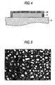
- the aforementioned agglomerate of the columnar crystal grains of tin oxide is formed so that the columns are aligned in the direction normal to the insulating layer surface, as shown in Fig. 3.
- This columnar crystal grain agglomerate can be confirmed by observing a section obtained by slicing the sensitive layer in the thickness direction of the substrate, magnified x500, 000 by a transmission electron microscope.
- the concentration of tin oxide crystals in the columnar agglomerate is usually 95% mass or more (including 100% mass) where the total mass of the tin oxide contained in the sensitive layer is 100% mass, but concentration is not limited to this.
- the average minor axis length (as indicated by d in Fig. 3 schematically presenting the minute structure of a section of the gas sensing element) of the columnar crystal grains is preferably 7 to 65 nm, more preferably 10 to 60 nm.
- the aforementioned average minor axis length of the columnar crystal grains can be determined in the following manner.
- a section which is obtained by slicing the sensitive layer in the direction of the thinnest dimension of the substrate is observed under magnification x500,000 by a transmission electron microscope (e.g., Type JEM-2010F of Nippon Denshi Kabushiki Gaisha) so that its dark field image is obtained.
- the minor axis lengths of arbitrary columnar crystal grains in the dark field image obtained are measured, and their average is adopted as the average minor axis length.
- the sensitive layer which is composed of that agglomerate of the columnar crystals of tin oxide.
- the sensitive layer can be manufactured by using a metal mask having the same opening as the shape of the desired sensitive layer and by depositing the composition of the sensitive layer at the desired portion of the surface of the insulating layer or the like.
- the catalytic portion is formed on the surface of the sensitive layer.
- the place where the catalytic portion is formed should not be limited to any position as long as it is on the surface of the sensitive layer.
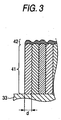
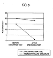
- the catalytic portion may be formed exclusively on the surface of the sensitive layer opposite to the surface contacting the insulating layer, as shown in Fig. 2, or may be formed to also cover the side surfaces of the sensitive layer, as shown in Fig. 4.
- the catalytic portion must have gas permeability. This gas permeability means that the oxidizing gas to be detected permeates to the surface of the sensitive layer.
- the method for forming the gas-permeable catalytic portion is not limited, and may be exemplified by a method forming the catalytic portions into island shape, as shown in Fig. 5.
- the aforementioned island shape means the shape in which island-shaped grains (i . e. , white portions in Fig. 5, hereafter called “island-shaped grains") composed mainly of gold (Au) are scattered on the surface of the sensitive layer (i.e. , black portions in Fig. 5).
- the average of the maximum sizes of one island-shaped grain in a planar direction can be 2 microns or less, preferably 1 micron or less.
- the average of the maximum size in the cross sectional direction can be 10 nm or more, preferably 20 nm or more.
- the mass thickness of the catalytic portion can be 0.008 to 170 nm, preferably 0.01 to 165 nm, more preferably 0.03 to 80 nm. If the mass thickness of the catalytic portion is 0.008 to 170 nm, a gas sensing element having sufficient sensitivity to the oxidizing gas and a catalytic portion having a sufficient gas-permeability can be formed, and thus this thickness is preferred.
- the mass thickness of the gold of the catalytic portion can be determined in the following manner.
- the gas sensing element is analyzed in the depth direction to obtain a profile of the various depths by an Auger electron spectroscopic analyzer (i.e., Field Emission Auger Microprobe: Type JAMP-7830F of Nippon Denshi Kabushiki Gaisha).
- Auger electron spectroscopic analyzer i.e., Field Emission Auger Microprobe: Type JAMP-7830F of Nippon Denshi Kabushiki Gaisha.
- the electron beam diameter is so set as to irradiate the gas sensing element as a whole with the electron beam.
- the dependence of distribution of gold at various depths on the etching time period can be found.
- the etching rate of SiO 2 is measured by employing a SiO 2 sample having a known film thickness.
- the etching rate of gold in a bulk shape is then determined by converting the etching rate of the SiO 2 measured.
- the mass thickness of the gold is calculated from the etching rate of gold obtained and the etching time found
- the above condition "composed mainly of gold” means that the concentration of gold is 80% mass or more (including the case of 100% mass) where the total mass of the catalytic portion is 100% mass.
- the area ratio of the sensitive layer covered by the catalytic portion is 1.5 to 93% when the gas sensing element is viewed in the direction passing through the thinnest dimension of the substrate. If the ratio of the area covering the sensitive layer is 1.5 to 93%, the sensitivity to the oxidizing gas is sufficient and the gas-permeability of the catalytic portion doesn't become low, and thus is preferred.
- the area ratio (or distribution percentage) of gold can be determined in the following manner.
- a reflected electron image is obtained by irradiating the upper portion of the gas sensing element with an electron beam in the direction passing through the thinnest dimension of the substrate by using a scanning type electron microscope (e.g., Type JSM-6330F of Nippon Denshi Kabushiki Gaisha).
- the reflected electron image obtained is an image in which gold is brighter than tin oxide.
- the area ratio (or distribution percentage) of gold on the surface of the sensitive layer is determined by processing the image of the reflected electron image obtained on the basis of the brightness.
- the method of forming the catalytic portion is not especially limited, but the catalytic portion can be formed by depositing the component for the catalytic portion on the surface of the sensitive layer and the insulating layer and then by etching the unnecessary portions.
- the oxidizing gas sensor of the invention is provided with the substrate.
- the material composing the substrate is usually a semiconductor, although not limited thereto. Of these materials, silicon is most frequently employed.
- the planar shape of the substrate is not limited and can be made into rectangular, circular, and other shapes.
- the size is not limited either, but preferably has a length of 0.1 to 10 mm and a width of 0.1 to 10 mm in case the shape is rectangular.
- the substrate preferably has an area equivalent to that of the rectangle.
- the substrate preferably has a thickness of 400 to 500 microns, although not limited thereto.
- the substrate is further provided with the open space portion.
- This open space portion is a portion where the substrate is partially cut away, reducing the thickness.
- This cut-away portion can be a through cavity (hereafter "cavity") which is opened both in the upper and lower surfaces of the substrate, or a recess which is opened in either the upper or the lower surfaces of the substrate. Of these, the cavity is preferred.
- the open shape is usually simple, for instance a rectangle or a circle.
- the size of the open space portion is not especially limited.
- the open space portion is a cavity, however, it is preferred that one of the two openings is formed to have a larger open area.
- the larger one has an open area of 0.01 to 4 mm 2 , preferably 0.25 to 2 mm 2 .
- the open area can be within a range like that of the aforementioned cavity.
- the method for forming the open space portion is not especially limited either, but the open space portion can be formed by etching off a portion of the substrate.
- the etching method to be used is not especially limited, and may be the wet etching method or the dry etching method (both being either anisotropic or isotropic etching). Of these, the wet etching method using an anisotropic etching liquid is generally used in case the aforementioned cavity is to be formed.
- the insulating layer is formed on the surface of the aforementioned substrate.
- This insulating layer is a layer for insulating the later-described electrodes electrically from the substrate.
- This insulating layer is formed on the surface of the substrate so as to cover the opening of the open space portion formed in the substrate and to be supported by the substrate.
- the insulating layer may be formed over the whole substrate or only part of the substrate, as long as it covers the opening of the open space portion and is supported by the substrate.
- the insulating layer is formed to cover the opening as a whole.
- the insulating layer may be formed to cover only a portion of the opening if the insulating layer can be supported by the substrate.
- the aforementioned word "supported” means that the insulating layer is supported by the substrate surface so as to cover the opening of the open space portion.
- the material of the insulating layer is not especially limited as long as the material has an insulating property, and may be a silicon compound such as SiO 2 , Si 3 N 4 and SiO x N y . Moreover, the insulating layer is not limited in its shape and thickness, and may be a single layer or a plurality of layers.
- the forming method of the insulating layer is not especially limited and can be, for example, a thermal-oxidation method modifying the surface of the substrate.
- the insulating layer can be obtained by depositing the components thereof on the surface of the substrate. Still moreover, the insulating layer can be obtained by adhering a previously prepared insulating layer to the surface of the substrate.
- the oxidizing gas sensor of the invention is provided with the heating element in the insulating layer.
- This heating element generates heat when fed with a voltage, and rises to a high temperature.
- the heating element activates the gas sensing element with its heat so that the measurement can be made.
- the heating element is usually connected with leads for feeding it with the electric power from an external circuit.
- the heating element is preferably arranged in the insulating layer and at a position corresponding to the open space portion of the substrate.
- the heat generated by the heating element can be prevented from dissipating from the heating element through the substrate when it is arranged at a position corresponding to the open space portion.
- the heating element can transmit the heat efficiently to the gas sensing element to raise the temperature of the gas sensing element more quickly and to control the temperature more precisely.
- the aforementioned position corresponding to the open space portion means the positional relation, in which the heating element and the open space portion at least partially overlap in the direction passing through the thinnest dimension of the substrate. In this case, the heating element lies in its entirety over the open space portion.
- the material for the heating element is not especially limited, as long as it has conductivity, but can be exemplified by pure platinum, a platinum alloy, a nickel alloy, a chromium alloy or a nickel-chromium alloy. Of these, pure platinum or the nickel-chromium alloy is preferably used because it has a large resistance-temperature coefficient so that its resistance and resistance-temperature coefficient hardly change even when it is repeatedly used for a long time.
- the heating element is not limited to a single layer structure but may be plural layers.
- a plural-layered heating element can be prepared, for example, by forming a Ta layer (having a thickness of 10 to 40 nm, for example) and then by forming a Pt layer (having a thickness of 150 to 350 nm, for example) .
- the heating element can be formed in the insulating layer by depositing a predetermined material on the surface of the insulating layer, and then removing the unnecessary portions by various etching methods as in the above open space portion forming process, and further by depositing another insulating layer on that upper surface.
- the oxidizing gas sensor of the invention is provided with electrodes to contact with the aforementioned sensitive layer.
- the electrode pair contacts the sensitive layer so as to apply voltage to the sensitive layer and to extract output signals.
- the electrodes are preferred to have a film thickness of equal to or less than that of the sensitive layer. This is because it is possible that the sensitive layer cannot be formed as a continuous layer if the electrodes have a larger film thickness than that of the sensitive layer.
- the material for the electrodes are not especially limited as long as it has a high conductivity, and can be Pt, Au, or Al, of which Pt is most desired. It is acceptable to use one exclusively or two or more together.
- the electrodes should not be limited to a single layer structure but may be a plurality of layers. Such plural-layered electrodes can be prepared by forming a Ti layer (having a film thickness of 10 to 40 nm, for example) and then by forming a Pt layer (having a film thickness of 10 to 70 nm, for example).
- the method for forming the electrodes is not especially limited, and the electrodes can be obtained by depositing a predetermined material on the insulating layer.
- the gas sensor of the embodiment is described on its construction. This gas sensor has dimensions (length x width) of 3 mm X 5 mm.
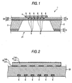
- the gas sensor 1 is constructed to have insulating layers 3 formed on the top and bottom surfaces of a silicon substrate 2 (as will be shortly called the "substrate 2"), as shown in Fig. 1.
- the insulating layers 3 are composed of an insulating layer 31 made of silicon oxide (SiO 2 ), and insulating layers 32 and 33 made of silicon nitride (Si 3 N 4 ) and laid over the insulating layer 31.
- this substrate 2 has an open space portion 21 formed so that it is opened at its upper surface on the side where the insulating layer 32 is formed.
- This opening in the open space portion 21 has an area of 1 mm 2 .
- a heating element 5 is formed over the open space portion 21. With this heating element 5, although not shown, there are connected lead portions for feeding the electric power. These lead portions have contacts for connections with an external circuit. These heating portions and their leads are made to have a two-layered structure composed of a Pt layer and a Ta layer.
- a pair of electrodes 6 is formed on the surface of the insulating layer 33 so as to be positioned over the heating element 5.
- a gas sensing element 4 is also formed on the surface of the insulating layer 33 over the heating element 5.
- the gas sensing element 4 is formed on the surface of the insulating layer 33 so as to contact with the upper faces of the electrodes 6.
- there are connected electrode lead portions which have electrode contacts for connections with an external circuit.
- the electrodes 6 are composed of a lower layer electrode 61, formed of Ti and positioned over the insulating layer 33, and an upper layer electrode 62 formed of Pt and positioned over the lower layer electrode 61.
- the lower layer electrode 61 has a film thickness of 20 nm
- the upper layer electrode 62 has a film thickness of 40 nm.
- the gas sensing element 4 is composed of a sensitive layer 41 made mainly of tin oxide (99% mass or more where the whole layer composition is 100% mass), and a catalytic portion 42 made of Au. On the other hand, the gas sensing element 4 is formed into a square planar shape having chamfered corners.
- the gas sensor of the embodiment was manufactured by the following process.
- a silicon substrate (having a thickness of 400 microns) for the substrate 2 was immersed in a rinsing liquid and subjected to a rinsing treatment.
- the silicon substrate was put into a heat treatment furnace and subj ected to a thermal-oxidation treatment to form a silicon oxide film as the insulating layer 31 having a film thickness of 100 nm all over the substrate 2.
- a silicon nitride film was formed as the insulating layer 32 (having a film thickness of 500 nm) on one face of the substrate 2, and a silicon nitride film (having a film thickness of 200 nm) was formed as a lower insulating layer 331 (see Fig. 1), i.e., the lower half of the insulating layer 33 on the other face.
- a Ta layer (having a film thickness of 25 nm) was then formed as the lower layer of the heating element 5 on the surface of that lower insulating layer 331, and a Pt layer (having a film thickness of 250 nm) was formed as the upper layer of the heating element 5 on the surface of that Ta layer.
- the resist was patterned by a photolithography, and the pattern of the heating element 5 was formed by etching treatment.
- an upper insulating layer 332 (having a film thickness of 500 nm, as shown in Fig. 1) which is the upper half of the insulating layer 33 was then formed by a method like the aforementioned one.
- the insulating layers 32 and 33 and the heating element 5 arranged in the insulating layer 33 were formed.
- the insulating layer 33 was etched by a dry etching method to form hole portions exposing the heater contacts to the outside.
- the Ti layer having a thickness of 20 nm
- the Pt layer having a thickness of 40 nm
- the resist was patterned by the photolithography to form the contacts for the heating elements.
- the Ti layer (having a thickness of 20 nm) was formed for the lower layer electrode 61, and the Pt layer (having a film thickness of 40 nm) was then formed for the upper layer electrode 62.
- the resists were patterned by the photolithography, and the upper layer electrode 62, the lower layer electrode 61, and the not-shown electrode leads and electrode contacts were formed.
- the DC sputtering apparatus was applied to the substrate to form the Cr layer (having a film thickness of 50 nm) for the lower layer of contact pads and then the Au layer (having a film thickness of 1 micron) for the upper layer of the contact pads.
- the resist was patterned by the photolithography and individual contact pads were formed over the not-shown contacts for the electrodes and the heating element by the etching treatment.
- the substrate After the substrate has finished the foregoing steps, it was immersed in a TMAH solution and was subjected to an anisotropic etching of silicon so that the open space portion 21 was formed at a position corresponding to the heating element 5, with its open face at the insulating layer 32.
- an RF sputtering apparatus was used to form the gas sensing element 4 on the upper surface of the insulating layer 33 at a position corresponding to the heating element 5 and the open space portion 21.
- a metal mask was used to form a tin oxide layer (having a film thickness of 200 nm) on the surface of the insulating layer 33 to be the sensitive layer 41, and then the Au layer on the surface of the tin oxide layer to be the catalytic portion 42.
- the tin oxide layer and the Au layer were formed by a method in which the substrate was heated to 350 °C to 500 °C) (the thermal-sputtering method),and by a method in which the tin oxide layer and the Au layer were formed on the substrate at the room temperature and in which the tin oxide layer and the Au layer were then heated and annealed at 350 °C to 700 °C for 3 hours(the room-temperature sputtering method).
- the film thickness of the Au layer was varied by varying the time period for film formation.
- the tin oxide layer was formed to have either a columnar structure or a microcrystalline structure. In the case where the tin oxide layer has columnar structure, moreover, the columnar crystals were varied in their minor axis length by varying the heating temperature or the heating-annealing temperature of the substrate.
- a SnO 2 target and an Au target were simultaneously sputtered to form a sensitive layer, in which the Au was homogeneously dispersed in the tin oxide layer.
- a gas sensor was manufactured like that of the above Embodiment, but with the simultaneous sputtering.
- the NO 2 sensitivity of the case of the NO 2 concentration of 1 ppm is 1.
- the catalytic portion made of Au was formed on the surface of the sensitive layer, it is found that the NO 2 sensitivity for the NO 2 concentration of 1 ppm is as high as 20.
- the present invention should not be limited to the disclosure of the specific embodiments thus far described but can bemodified into various embodiments within the scope thereof in accordance with its object and application.
- the catalytic portion is formed on the upper face of the sensitive layer, but its place is not especially restricted as long as it is on the surface of the sensitive layer.
Landscapes
- Chemical & Material Sciences (AREA)
- Chemical Kinetics & Catalysis (AREA)
- Electrochemistry (AREA)
- Physics & Mathematics (AREA)
- Health & Medical Sciences (AREA)
- Life Sciences & Earth Sciences (AREA)
- Analytical Chemistry (AREA)
- Biochemistry (AREA)
- General Health & Medical Sciences (AREA)
- General Physics & Mathematics (AREA)
- Immunology (AREA)
- Pathology (AREA)
- Investigating Or Analyzing Materials By The Use Of Fluid Adsorption Or Reactions (AREA)
Abstract
Description
| Gas Sensing Element | NO2 Sensitivity | |
| Embodiment | Two-Layered | 20 |
| Comparison | Au Dispersed | 1 |
| Au Mass Film Thickness (nm) | Distribution of Au (%) | NO2 Sensed | Method of GSE | |
| TE1 | 0.005 | 97 | 3 | H-Spt |
| TE2 | 0.01 | 1 | 5 | RT-Spt |
| TE3 | 0.01 | 90 | 8 | H-Spt |
| TE4 | 0.03 | 85 | 16 | H-Spt |
| TE5 | 0.05 | 2 | 25 | RT-Spt |
| TE6 | 0.1 | 90 | 20 | H-Spt |
| TE7 | 0.1 | 24 | 24 | RT- |
| TE8 | ||||
| 3 | 91 | 30 | H- | |
| TE9 | ||||
| 4 | 36 | 20 | RT-Spt | |
| TE10 | 4.5 | 92 | 40 | H-Spt |
| TE11 | 5.4 | 80 | 30 | RT-Spt |
| TE12 | 14 | 90 | 35 | H-Spt |
| TE13 | 48 | 80 | 27 | H-Spt |
| TE14 | 80 | 85 | 15 | H-Spt |
| TE15 | 82.8 | 75 | 10 | H-Spt |
| TE16 | 165 | 80 | 8 | RT-Spt |
| TE17 | 165 | 95 | 5 | H-Spt |
| TE18 | 250 | 99 | 2 | H-Spt |
| NO2 sensitivity Before Tests | NO2 sensitivity After | |
| Columnar Structure | ||
| 20 | 18 | |
| | 15 | 5 |
| AMAL(nm) of SnO2 | NO2 Sensed | | |
| TE19 | |||
| 2 | 2 | H-Spt (Substrate Temp.:500 °C) | |
| | 5 | 4 | H-Spt (Substrate Temp.:450 °C) |
| | 10 | 15 | H-Spt (Substrate Temp.:350 °C) |
| | 15 | 45 | RT-Spt (Annealing:350 °C) |
| TE23 | 30 | 35 | RT-Spt (Annealing:400 °C) |
| TE24 | 60 | 20 | RT-Spt (Annealing:500 °C) |
| TE25 | 70 | 4 | RT-Spt (Annealing:600 °C) |
| TE26 | 80 | 2 | RT-Spt (Annealing:700 °C) |
Claims (4)
- An oxidizing gas sensor comprising:characterized in that said gas sensing element includes a sensitive layer composed mainly of tin oxide, and a gas-permeable catalytic portion formed mainly of gold at least on a portion of the surface of said sensitive layer and having gas permeability.a substrate having an open space portion in which the thickness is reduced;an insulating layer formed on the surface of said substrate so as to cover said open space portion;a heating element formed in said insulating layer at a position corresponding to said open space portion;a gas sensing element formed on the surface of said insulating layer at a position corresponding to said heating element; anda pair of electrodes disposed to contact said gas sensing element,
- An oxidizing gas sensor as set forth in claim 1, characterized in that said catalytic portion has amass thickness of 0.008 to 170 nm.
- An oxidizing gas sensor as set forth in claim 2, characterized in that said catalytic portion is formed to cover 1.5 to 93 % of the area of said sensitive layer, viewing the gas sensing element is in the direction passing through the thinnest dimension of said substrate.
- An oxidizing gas sensor as set forth in claim 3, characterized: in that the structure of said sensitive layer is an agglomerate of tin oxide columnar crystal grains; and in that said crystal grains have an average minor axis length of 7 to 65 nm.
Applications Claiming Priority (3)
| Application Number | Priority Date | Filing Date | Title |
|---|---|---|---|
| JP2002344585 | 2002-11-27 | ||
| JP2002344585 | 2002-11-27 | ||
| PCT/JP2003/015098 WO2004048957A1 (en) | 2002-11-27 | 2003-11-26 | Oxidizing gas sensor |
Publications (3)
| Publication Number | Publication Date |
|---|---|
| EP1568990A1 true EP1568990A1 (en) | 2005-08-31 |
| EP1568990A4 EP1568990A4 (en) | 2007-04-25 |
| EP1568990B1 EP1568990B1 (en) | 2016-06-22 |
Family
ID=32375959
Family Applications (1)
| Application Number | Title | Priority Date | Filing Date |
|---|---|---|---|
| EP03811929.3A Expired - Lifetime EP1568990B1 (en) | 2002-11-27 | 2003-11-26 | Oxidizing gas sensor |
Country Status (5)
| Country | Link |
|---|---|
| EP (1) | EP1568990B1 (en) |
| JP (1) | JP4219330B2 (en) |
| KR (1) | KR100990798B1 (en) |
| AU (1) | AU2003302452A1 (en) |
| WO (1) | WO2004048957A1 (en) |
Cited By (4)
| Publication number | Priority date | Publication date | Assignee | Title |
|---|---|---|---|---|
| EP1696229A1 (en) * | 2005-02-24 | 2006-08-30 | Ngk Spark Plug Co., Ltd | Oxidizing gas sensor and production method thereof |
| EP1688714A3 (en) * | 2005-02-07 | 2006-10-18 | Ngk Spark Plug Co., Ltd | Micro-heater and sensor |
| RU2319953C1 (en) * | 2006-08-15 | 2008-03-20 | Общество с ограниченной ответственностью Научно-производственное предприятие "Сенсерия" | Method of manufacturing sensor for semiconductive gas transducer |
| RU219451U1 (en) * | 2023-04-24 | 2023-07-18 | Владимир Михайлович Фрейман | Measuring probe for determining the concentration of hydrogen and carbon monoxide dissolved in industrial oils |
Families Citing this family (6)
| Publication number | Priority date | Publication date | Assignee | Title |
|---|---|---|---|---|
| JP4779656B2 (en) * | 2006-01-11 | 2011-09-28 | ソニー株式会社 | Gas sensor |
| US8683847B2 (en) | 2011-02-09 | 2014-04-01 | Electronics And Telecommunications Research Institute | Microelectromechanical systems type semiconductor gas sensor using microheater having many holes and method for manufacturing the same |
| DE102013212478A1 (en) * | 2013-06-27 | 2014-12-31 | Robert Bosch Gmbh | gas sensor |
| KR20160120437A (en) * | 2015-04-08 | 2016-10-18 | 남성원 | Oxygen and carbon dioxide gas real-time detecting sensor and a method of manufacturing the gas sensors and the detection method of the gas composition within the packaging container using the same |
| KR102438194B1 (en) * | 2016-01-27 | 2022-08-31 | 주식회사 디비하이텍 | Semiconductor gas sensor and manufacturing method thereof |
| JP2024031065A (en) * | 2022-08-25 | 2024-03-07 | 国立大学法人 東京大学 | Membrane for gas sensor, method for manufacturing gas sensor membrane, gas sensor, method for manufacturing gas sensor, and method for manufacturing catalyst part |
Family Cites Families (11)
| Publication number | Priority date | Publication date | Assignee | Title |
|---|---|---|---|---|
| US4706493A (en) * | 1985-12-13 | 1987-11-17 | General Motors Corporation | Semiconductor gas sensor having thermally isolated site |
| JPH0643978B2 (en) * | 1986-06-27 | 1994-06-08 | 大阪瓦斯株式会社 | Gas sensor and manufacturing method thereof |
| JPH02263148A (en) * | 1988-12-27 | 1990-10-25 | Kurabe:Kk | Gaseous carbon monoxide detecting element |
| JP2829416B2 (en) * | 1989-07-28 | 1998-11-25 | 株式会社クラベ | Gas sensing element |
| JPH0545321A (en) * | 1991-08-10 | 1993-02-23 | Kurabe Ind Co Ltd | Gas sensor |
| JPH07140101A (en) * | 1993-11-19 | 1995-06-02 | Fuji Electric Co Ltd | Incomplete combustion gas sensor |
| JP2582343B2 (en) * | 1993-12-04 | 1997-02-19 | エルジー電子株式会社 | Low power consumption thin film gas sensor and method of manufacturing the same |
| DE4445359A1 (en) * | 1994-12-20 | 1996-06-27 | Bosch Gmbh Robert | Sensor for the detection of flammable gases |
| JPH0996622A (en) | 1995-09-29 | 1997-04-08 | Matsushita Electric Ind Co Ltd | Gas sensor and manufacturing method thereof |
| JP2000258374A (en) * | 1999-03-09 | 2000-09-22 | Fuji Electric Co Ltd | Thin-film gas sensor and gas alarm using the same |
| JP2000298108A (en) * | 1999-04-13 | 2000-10-24 | Osaka Gas Co Ltd | Gas sensor |
-
2003
- 2003-11-26 KR KR1020057008125A patent/KR100990798B1/en not_active Expired - Fee Related
- 2003-11-26 AU AU2003302452A patent/AU2003302452A1/en not_active Abandoned
- 2003-11-26 JP JP2004555053A patent/JP4219330B2/en not_active Expired - Fee Related
- 2003-11-26 WO PCT/JP2003/015098 patent/WO2004048957A1/en not_active Ceased
- 2003-11-26 EP EP03811929.3A patent/EP1568990B1/en not_active Expired - Lifetime
Cited By (6)
| Publication number | Priority date | Publication date | Assignee | Title |
|---|---|---|---|---|
| EP1688714A3 (en) * | 2005-02-07 | 2006-10-18 | Ngk Spark Plug Co., Ltd | Micro-heater and sensor |
| US7487675B2 (en) | 2005-02-07 | 2009-02-10 | Ngk Spark Plug Co., Ltd. | Micro-heater and sensor |
| EP1696229A1 (en) * | 2005-02-24 | 2006-08-30 | Ngk Spark Plug Co., Ltd | Oxidizing gas sensor and production method thereof |
| US7412871B2 (en) | 2005-02-24 | 2008-08-19 | Ngk Spark Plug Co., Ltd. | Oxidizing gas sensor and production method thereof |
| RU2319953C1 (en) * | 2006-08-15 | 2008-03-20 | Общество с ограниченной ответственностью Научно-производственное предприятие "Сенсерия" | Method of manufacturing sensor for semiconductive gas transducer |
| RU219451U1 (en) * | 2023-04-24 | 2023-07-18 | Владимир Михайлович Фрейман | Measuring probe for determining the concentration of hydrogen and carbon monoxide dissolved in industrial oils |
Also Published As
| Publication number | Publication date |
|---|---|
| EP1568990A4 (en) | 2007-04-25 |
| JP4219330B2 (en) | 2009-02-04 |
| JPWO2004048957A1 (en) | 2006-03-23 |
| KR100990798B1 (en) | 2010-10-29 |
| AU2003302452A1 (en) | 2004-06-18 |
| EP1568990B1 (en) | 2016-06-22 |
| KR20050084980A (en) | 2005-08-29 |
| WO2004048957A1 (en) | 2004-06-10 |
Similar Documents
| Publication | Publication Date | Title |
|---|---|---|
| EP4102216B1 (en) | Multi-dimensional multi-parameter gas sensor and manufacturing method therefor, and gas detection method | |
| EP3615926B1 (en) | Gas sensors including microhotplates with resistive heaters, and related methods | |
| US7828480B2 (en) | Thermocouple circuit and method and system for forming same | |
| US4953387A (en) | Ultrathin-film gas detector | |
| US6109094A (en) | Method and device for gas sensing | |
| US6290388B1 (en) | Multi-purpose integrated intensive variable sensor | |
| US20030037590A1 (en) | Method of self-testing a semiconductor chemical gas sensor including an embedded temperature sensor | |
| EP1696229B1 (en) | Oxidizing gas sensor and production method thereof | |
| JP4265912B2 (en) | Thin film ppb oxygen sensor | |
| Arshak et al. | Investigation of tin oxides as sensing layers in conductimetric interdigitated pH sensors | |
| EP1568990B1 (en) | Oxidizing gas sensor | |
| JP2006324520A (en) | Thermistor thin film and manufacturing method thereof | |
| EP0464243B1 (en) | Oxygen sensor with semiconducting gallium oxide | |
| WO2020100778A1 (en) | Condensation detection element | |
| DE19941420A1 (en) | Electrical resistor, such as temperature dependent resistor used as measuring resistor has conducting path with connecting contact fields arranged on an electrically insulating surface of substrate | |
| DE3844023A1 (en) | SENSOR FOR DETERMINING THE GAS CONCENTRATION IN A GAS MIXTURE BY MEASURING THE HEAT | |
| JPH0714904A (en) | Method and circuit for measuring flatness of dielectric layer in integrated circuit | |
| DE102021213046B3 (en) | Sensor, sensor system and method for detecting thermodynamic parameters of a sample and the use of the sensor or sensor system | |
| CN117099172A (en) | Strain resistor film, pressure sensor and laminate | |
| US6127193A (en) | Test structure used to measure metal bottom coverage in trenches and vias/contacts and method for creating the test structure | |
| US20020175379A1 (en) | Polysilicon resistor semiconductor device | |
| Wollenstein et al. | Preparation, morphology, and gas-sensing behavior of Cr/sub 2-x/Ti/sub x/O/sub 3+ z/thin films on standard silicon wafers | |
| KR100896482B1 (en) | Gas sensor using thermal sensor and its manufacturing method | |
| KR940002637B1 (en) | Oxygen sensor | |
| EP4356086B1 (en) | Sensor, sensor system and method for measuring thermodynamic parameters of a sample, and use of the sensor or sensor system |
Legal Events
| Date | Code | Title | Description |
|---|---|---|---|
| PUAI | Public reference made under article 153(3) epc to a published international application that has entered the european phase |
Free format text: ORIGINAL CODE: 0009012 |
|
| 17P | Request for examination filed |
Effective date: 20050620 |
|
| AK | Designated contracting states |
Kind code of ref document: A1 Designated state(s): AT BE BG CH CY CZ DE DK EE ES FI FR GB GR HU IE IT LI LU MC NL PT RO SE SI SK TR |
|
| AX | Request for extension of the european patent |
Extension state: AL LT LV MK |
|
| DAX | Request for extension of the european patent (deleted) | ||
| RBV | Designated contracting states (corrected) |
Designated state(s): DE FR |
|
| A4 | Supplementary search report drawn up and despatched |
Effective date: 20070327 |
|
| 17Q | First examination report despatched |
Effective date: 20080225 |
|
| GRAP | Despatch of communication of intention to grant a patent |
Free format text: ORIGINAL CODE: EPIDOSNIGR1 |
|
| INTG | Intention to grant announced |
Effective date: 20160210 |
|
| GRAS | Grant fee paid |
Free format text: ORIGINAL CODE: EPIDOSNIGR3 |
|
| GRAA | (expected) grant |
Free format text: ORIGINAL CODE: 0009210 |
|
| AK | Designated contracting states |
Kind code of ref document: B1 Designated state(s): DE FR |
|
| REG | Reference to a national code |
Ref country code: DE Ref legal event code: R096 Ref document number: 60349069 Country of ref document: DE |
|
| REG | Reference to a national code |
Ref country code: FR Ref legal event code: PLFP Year of fee payment: 14 |
|
| REG | Reference to a national code |
Ref country code: DE Ref legal event code: R097 Ref document number: 60349069 Country of ref document: DE |
|
| PLBE | No opposition filed within time limit |
Free format text: ORIGINAL CODE: 0009261 |
|
| STAA | Information on the status of an ep patent application or granted ep patent |
Free format text: STATUS: NO OPPOSITION FILED WITHIN TIME LIMIT |
|
| 26N | No opposition filed |
Effective date: 20170323 |
|
| REG | Reference to a national code |
Ref country code: FR Ref legal event code: PLFP Year of fee payment: 15 |
|
| REG | Reference to a national code |
Ref country code: FR Ref legal event code: PLFP Year of fee payment: 16 |
|
| PGFP | Annual fee paid to national office [announced via postgrant information from national office to epo] |
Ref country code: DE Payment date: 20191112 Year of fee payment: 17 |
|
| PGFP | Annual fee paid to national office [announced via postgrant information from national office to epo] |
Ref country code: FR Payment date: 20191014 Year of fee payment: 17 |
|
| REG | Reference to a national code |
Ref country code: DE Ref legal event code: R119 Ref document number: 60349069 Country of ref document: DE |
|
| PG25 | Lapsed in a contracting state [announced via postgrant information from national office to epo] |
Ref country code: FR Free format text: LAPSE BECAUSE OF NON-PAYMENT OF DUE FEES Effective date: 20201130 |
|
| PG25 | Lapsed in a contracting state [announced via postgrant information from national office to epo] |
Ref country code: DE Free format text: LAPSE BECAUSE OF NON-PAYMENT OF DUE FEES Effective date: 20210601 |