EP1568657A2 - Method of manufacturing nanostructure arrays - Google Patents
Method of manufacturing nanostructure arrays Download PDFInfo
- Publication number
- EP1568657A2 EP1568657A2 EP05251031A EP05251031A EP1568657A2 EP 1568657 A2 EP1568657 A2 EP 1568657A2 EP 05251031 A EP05251031 A EP 05251031A EP 05251031 A EP05251031 A EP 05251031A EP 1568657 A2 EP1568657 A2 EP 1568657A2
- Authority
- EP
- European Patent Office
- Prior art keywords
- species
- substrate
- milling
- onto
- pores
- Prior art date
- Legal status (The legal status is an assumption and is not a legal conclusion. Google has not performed a legal analysis and makes no representation as to the accuracy of the status listed.)
- Withdrawn
Links
Images

Classifications
-
- B—PERFORMING OPERATIONS; TRANSPORTING
- B81—MICROSTRUCTURAL TECHNOLOGY
- B81C—PROCESSES OR APPARATUS SPECIALLY ADAPTED FOR THE MANUFACTURE OR TREATMENT OF MICROSTRUCTURAL DEVICES OR SYSTEMS
- B81C1/00—Manufacture or treatment of devices or systems in or on a substrate
- B81C1/00436—Shaping materials, i.e. techniques for structuring the substrate or the layers on the substrate
- B81C1/00555—Achieving a desired geometry, i.e. controlling etch rates, anisotropy or selectivity
- B81C1/00611—Processes for the planarisation of structures
-
- B—PERFORMING OPERATIONS; TRANSPORTING
- B82—NANOTECHNOLOGY
- B82Y—SPECIFIC USES OR APPLICATIONS OF NANOSTRUCTURES; MEASUREMENT OR ANALYSIS OF NANOSTRUCTURES; MANUFACTURE OR TREATMENT OF NANOSTRUCTURES
- B82Y10/00—Nanotechnology for information processing, storage or transmission, e.g. quantum computing or single electron logic
-
- B—PERFORMING OPERATIONS; TRANSPORTING
- B82—NANOTECHNOLOGY
- B82Y—SPECIFIC USES OR APPLICATIONS OF NANOSTRUCTURES; MEASUREMENT OR ANALYSIS OF NANOSTRUCTURES; MANUFACTURE OR TREATMENT OF NANOSTRUCTURES
- B82Y30/00—Nanotechnology for materials or surface science, e.g. nanocomposites
-
- G—PHYSICS
- G11—INFORMATION STORAGE
- G11B—INFORMATION STORAGE BASED ON RELATIVE MOVEMENT BETWEEN RECORD CARRIER AND TRANSDUCER
- G11B5/00—Recording by magnetisation or demagnetisation of a record carrier; Reproducing by magnetic means; Record carriers therefor
- G11B5/62—Record carriers characterised by the selection of the material
- G11B5/73—Base layers, i.e. all non-magnetic layers lying under a lowermost magnetic recording layer, e.g. including any non-magnetic layer in between a first magnetic recording layer and either an underlying substrate or a soft magnetic underlayer
- G11B5/739—Magnetic recording media substrates
- G11B5/73911—Inorganic substrates
- G11B5/73913—Composites or coated substrates
- G11B5/73915—Silicon compound based coating
-
- G—PHYSICS
- G11—INFORMATION STORAGE
- G11B—INFORMATION STORAGE BASED ON RELATIVE MOVEMENT BETWEEN RECORD CARRIER AND TRANSDUCER
- G11B5/00—Recording by magnetisation or demagnetisation of a record carrier; Reproducing by magnetic means; Record carriers therefor
- G11B5/62—Record carriers characterised by the selection of the material
- G11B5/73—Base layers, i.e. all non-magnetic layers lying under a lowermost magnetic recording layer, e.g. including any non-magnetic layer in between a first magnetic recording layer and either an underlying substrate or a soft magnetic underlayer
- G11B5/739—Magnetic recording media substrates
- G11B5/73911—Inorganic substrates
- G11B5/73921—Glass or ceramic substrates
-
- G—PHYSICS
- G11—INFORMATION STORAGE
- G11B—INFORMATION STORAGE BASED ON RELATIVE MOVEMENT BETWEEN RECORD CARRIER AND TRANSDUCER
- G11B5/00—Recording by magnetisation or demagnetisation of a record carrier; Reproducing by magnetic means; Record carriers therefor
- G11B5/84—Processes or apparatus specially adapted for manufacturing record carriers
- G11B5/855—Coating only part of a support with a magnetic layer
-
- B—PERFORMING OPERATIONS; TRANSPORTING
- B81—MICROSTRUCTURAL TECHNOLOGY
- B81C—PROCESSES OR APPARATUS SPECIALLY ADAPTED FOR THE MANUFACTURE OR TREATMENT OF MICROSTRUCTURAL DEVICES OR SYSTEMS
- B81C2201/00—Manufacture or treatment of microstructural devices or systems
- B81C2201/01—Manufacture or treatment of microstructural devices or systems in or on a substrate
- B81C2201/0101—Shaping material; Structuring the bulk substrate or layers on the substrate; Film patterning
- B81C2201/0118—Processes for the planarization of structures
- B81C2201/0121—Processes for the planarization of structures involving addition of material followed by removal of parts of said material, i.e. subtractive planarization
-
- G—PHYSICS
- G11—INFORMATION STORAGE
- G11B—INFORMATION STORAGE BASED ON RELATIVE MOVEMENT BETWEEN RECORD CARRIER AND TRANSDUCER
- G11B5/00—Recording by magnetisation or demagnetisation of a record carrier; Reproducing by magnetic means; Record carriers therefor
- G11B5/84—Processes or apparatus specially adapted for manufacturing record carriers
- G11B5/85—Coating a support with a magnetic layer by vapour deposition
Definitions
- the present invention relates to a method of manufacturing nanostructure arrays.
- Nanostructure is a material structure assembled from a layer or cluster of atoms. Nanostructures are typically sized in nanometers and include quantum dots, quantum wires, nanotubes, nanocrystals, and ultra-thin multilayer films. Many materials exhibit novel optical, electrical and/or optical behaviour at sizes below a few hundred nanometers as quantum mechanical principles begin to dominate material properties. The increased surface area of nanostructures compared with conventional materials is of particular interest to storage device designers because it provides the possibility for increased storage density.
- High surface areas can be attained either by fabricating small particles or clusters where the surface-to-volume ratio of each particle is high, or by creating materials where the void surface area (pores) is high compared to the amount of bulk support material.
- top-down fabrication techniques nanostructures are created by carving, moulding or machining bulk and thin film materials with tools and lasers. Top-down techniques include mechanical milling, photolithography and e-beam lithography.
- bottom-up fabrication techniques nanostructures are spontaneously built up from individual atoms or molecules or formed from chemical reordering of a material. These techniques are also known as self-assembly or self-ordering techniques and include gas condensation, chemical precipitation, aerosol reactions and biological templating.
- Anodization is a well-known self-assembly technique and the method of forming alumina by anodizing aluminium is particularly well-known.
- an aluminium foil is anodized using a suitable acid to produce a porous alumina membrane.
- the membrane has a geometrical structure determined by the anodizing conditions so that the pores may be regularly or irregularly formed in the membrane with diameters ranging from a few nanometers to several hundred nanometers.
- a double anodization technique may be used in which the first anodization is stopped and subsequently restarted after removal of the initially anodized material.
- an imprint technique may be used to pre-form the surface prior to anodization (Masuda et al, Science, 268(5216), 1466-1468 (1995) and Asoh et al, J.Vac.Sci.Technol. B, 19(2), 569-572,(2001)).
- the pore structure formed by the anodizing technique may be used as a template through which materials may be deposited (Liu et al, Appl.Phys.Lett. Vol.81(23), 4434-4436,(2002)). Prior to anodization, aluminium may be deposited by physical vapour deposition onto a planar substrate which had previously been coated with a material to act as a backing plate. This pre-processing step enables growth up into the pores after anodizing by electrodepositing onto the backing plate (Choi et al, J.Mater.Chem. Vol. 13(5), 1100-1103,(2003)).
- a method of disposing a plurality of isolated particles of a first material onto a substrate comprising the steps of:
- the substrate is glass.
- the substrate is silicon.
- the substrate is a conducting species.
- the first species is aluminium.
- the first species is deposited onto the substrate by physical vapour deposition.
- the first species is deposited onto the substrate by chemical vapour deposition.
- the first species is deposited onto the substrate in a thickness not less than 20nm.
- a third species is deposited onto the substrate before the first species.
- the deposited first species is treated before the anodization process to ensure a desired anodization pattern.
- the surface of the second species is altered by ion milling.
- the surface of the second species is altered by reactive ion etching.
- the surface of the second species is altered by atom milling.
- the surface of the second species is altered by a milling means disposed at an angle of incidence of between 0° and 60° measured from the normal to the surface of the substrate.
- each of the at least one second regions of the second species surrounds one of an at least one pores in the second species resulting from the anodization process.
- the at least one first regions of the second species are disposed between each of the at least one pores in the second species resulting from the anodization process.
- the first material is deposited onto the surface of the second species by physical vapour deposition.
- the first material comprises at least one layer of at least one species.
- the surface of the first material and the second species are levelled by ion milling.
- the surface of the first material and the second species are levelled by atom milling.
- the surface of the first material and the second species are levelled by a milling means disposed at an angle of incidence between 30° to 90° measured from the substrate surface normal.
- the present manufacturing method takes the novel and inventive approach of combining techniques to produce a nanoarray by physical vapour deposition, anodization and ion milling. Consequently, the present manufacturing method offers a way of creating patterned media that removes the need for lithographic techniques and is thus of particular benefit for high-density recording systems design.
- the method of disposing a plurality of isolated particles of a first material onto a substrate will be known henceforth as the manufacturing method.
- the manufacturing method is divided into five steps as follows:
- Step 1 Depositing Aluminium onto a Suitable Substrate
- a layer of aluminium 1 is deposited onto a suitable substrate 2 by physical vapour or chemical vapour deposition.
- the substrate may be an insulating material such as glass, a semi-conducting material such as silicon or a metal.
- the deposited aluminium layer should be no less than 20nm in thickness.
- an underlayer, conducting layer or combination of layers may be deposited onto the substrate 2 prior to the deposition of the aluminium layer 1.
- the aluminium layer 1 is anodized in a suitable acid.
- the anodization may be carried out as a single or two-stage process, although it is not necessary to completely anodize the aluminium layer 1.
- the aluminium layer 1 Prior to the anodization step, the aluminium layer 1 may also be treated by imprinting (or other method) to produce a desired pore 4 pattern.
- the aluminium layer 1 is converted into a non-uniformly dense alumina membrane 3 with regularly or irregularly disposed pores 4.
- Step 3 Ion/Atom Milling the Surface of the Anodized Alumina Layer to Produce a Topographical Surface
- the surface of the porous alumina membrane 3 is subjected to ion/atom milling.
- the milling technique employs an ion/atom source (e.g. Kaufmann type) with an appropriate gas (e.g. inert such as argon, krypton or other O 2 , N 2 ) to remove material from the surface of the porous alumina membrane 3.
- an ion/atom source e.g. Kaufmann type
- an appropriate gas e.g. inert such as argon, krypton or other O 2 , N 2
- the ion beam should be directed at the surface of the porous alumina membrane 3 with an angle of incidence of between 0° to 60° measured from the substrate surface normal.
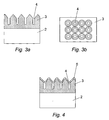
- the milling causes preferential etching closer to the pores 4 so that (referring to Figure 3(b)) the region of the porous alumina membrane 3 closest to the pores 4 is milled down to a reduced height whilst the region in-between the pores 4 is less affected (i.e. remains high). Referring to Figure 3(a), this results in a characteristic saw-wave pattern on the surface of the porous alumina membrane 3.
- Step 4 Physical Vapour Deposition of a material onto the Milled Anodized Alumina Surface
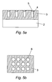
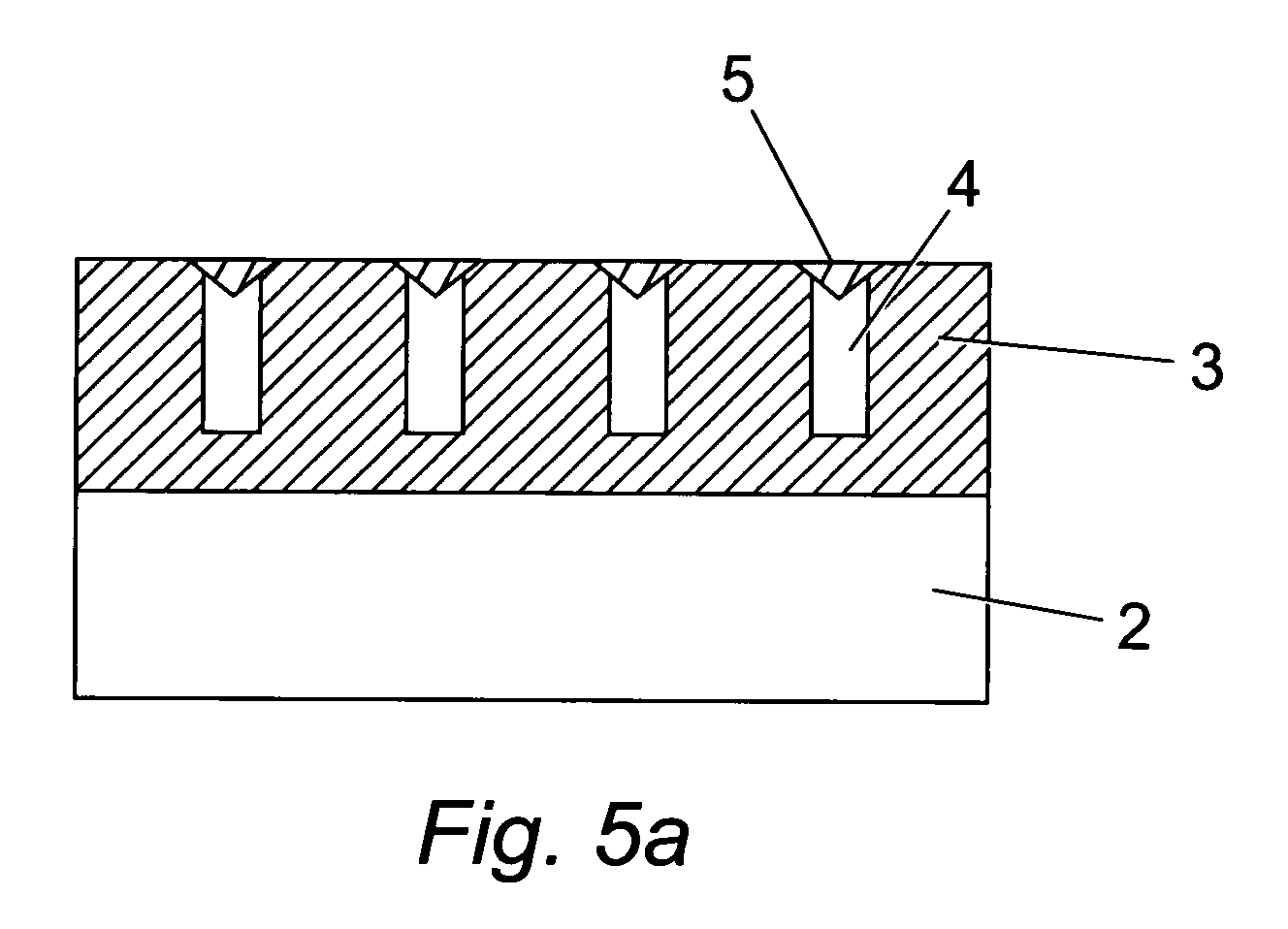
- a material 5 is physically vapour deposited (e.g. sputtering) onto the saw-wave surface of the milled porous alumina membrane 3.
- the material 5 may be a single layered (e.g. Au, CoPt alloy, BaTi0 3 compound) or a complex layered material (e.g. Co/Pt multilayer).
- the material 5 is deposited conformally over the elevated portions of the milled porous alumina membrane 3 (i.e. in the region between the pores 4) and remains connected over the pores 4.
- Step 5 Oblique Milling of Surface Resulting from Step 4 to Form and Planarize the Surface of an Array
- the surface of the vapour deposited material 5 is subjected to ion/atom milling at an oblique angle of incidence (i.e. wherein the milling angle is between 30° to 90° from the surface normal).
- This process removes the elevated regions of the material 5 and the porous alumina membrane 3 so that the resulting planar alumina surface contains isolated nano-particles 6 of material 5 located above each pore 4 formed during the anodization step.
Landscapes
- Engineering & Computer Science (AREA)
- Chemical & Material Sciences (AREA)
- Nanotechnology (AREA)
- Inorganic Chemistry (AREA)
- Physics & Mathematics (AREA)
- Crystallography & Structural Chemistry (AREA)
- Geometry (AREA)
- Microelectronics & Electronic Packaging (AREA)
- Ceramic Engineering (AREA)
- Manufacturing & Machinery (AREA)
- Condensed Matter Physics & Semiconductors (AREA)
- Materials Engineering (AREA)
- General Physics & Mathematics (AREA)
- Composite Materials (AREA)
- Mathematical Physics (AREA)
- Theoretical Computer Science (AREA)
- Physical Vapour Deposition (AREA)
- Internal Circuitry In Semiconductor Integrated Circuit Devices (AREA)
- Chemical Vapour Deposition (AREA)
Abstract
Description
- step 1:
- depositing aluminium onto a suitable substrate;
- step 2:
- anodizing the aluminium deposit;
- step 3:
- ion/atom milling the surface of the anodized alumina to produce a topographical surface;
- step 4:
- physical vapour deposition of a material onto the milled anodized alumina surface; and
- step 5:
- oblique milling of surface resulting
from
step 4 to form and planarize the surface of an array.
Claims (15)
- A method of disposing a plurality of isolated particles of a first material onto a substrate comprising the steps of:(a) depositing a first species onto the substrate;(b) anodizing the first species to produce a second species;(c) altering the surface of the second species so that at least one first region of the second species is of greater thickness than at least one second region of the second species;(d) depositing the first material onto the second species; and(e) levelling the surface of the first material and the second species.
- A method as claimed in claim 1 wherein the substrate is a substance selected from the group comprising glass, silicon and a conducting substance.
- A method as claimed in claim 1 or 2 wherein the first species is aluminium.
- A method as claimed in any of the preceding claims wherein the first species is deposited onto the substrate by a procedure selected from the group comprising physical vapour deposition and chemical vapour deposition.
- A method as claimed in any of the preceding claims wherein the first species is deposited onto the substrate in a thickness not less than 20nm.
- A method as claimed in any of the preceding claims wherein a third species is deposited onto the substrate before the first species.
- A method as claimed in any of the preceding claims wherein the deposited first species is treated before the anodization process to ensure a desired anodization pattern.
- A method as claimed in any of the preceding claims wherein the surface of the second species is altered by a procedure selected from the group comprising ion milling, reactive ion etching and atom milling.
- A method as claimed in any claim 8 wherein the surface of the second species is altered by a milling means disposed at an angle of incidence of between 0° and 60° measured from the normal to the surface of the substrate.
- A method as claimed in any of the preceding claims wherein each of the at least one second regions of the second species surrounds one of an at least one pores in the second species resulting from the anodization process.
- A method as claimed in any of the preceding claims wherein the at least one first regions of the second species are disposed between each of the at least one pores in the second species resulting from the anodization process.
- A method as claimed in any of the preceding claims wherein the first material is deposited onto the surface of the second species by physical vapour deposition.
- A method as claimed in any of the preceding claims wherein the first material comprises at least one layer of at least one species.
- A method as claimed in any of the preceding claims wherein the surface of the first material and the second species are levelled by a procedure selected from the group comprising ion milling and atom milling.
- A method as claimed in claim 14 wherein the surface of the first material and the second species are levelled by a milling means disposed at an angle of incidence between 30° to 90° measured from the substrate surface normal.
Applications Claiming Priority (2)
| Application Number | Priority Date | Filing Date | Title |
|---|---|---|---|
| GBGB0404120.8A GB0404120D0 (en) | 2004-02-25 | 2004-02-25 | Method of manufacturing nanostructure arrays |
| GB0404120 | 2004-02-25 |
Publications (2)
| Publication Number | Publication Date |
|---|---|
| EP1568657A2 true EP1568657A2 (en) | 2005-08-31 |
| EP1568657A3 EP1568657A3 (en) | 2006-07-26 |
Family
ID=32050800
Family Applications (1)
| Application Number | Title | Priority Date | Filing Date |
|---|---|---|---|
| EP05251031A Withdrawn EP1568657A3 (en) | 2004-02-25 | 2005-02-23 | Method of manufacturing nanostructure arrays |
Country Status (2)
| Country | Link |
|---|---|
| EP (1) | EP1568657A3 (en) |
| GB (1) | GB0404120D0 (en) |
Family Cites Families (3)
| Publication number | Priority date | Publication date | Assignee | Title |
|---|---|---|---|---|
| JP3902883B2 (en) * | 1998-03-27 | 2007-04-11 | キヤノン株式会社 | Nanostructure and manufacturing method thereof |
| JP2002084019A (en) * | 2000-09-08 | 2002-03-22 | Canon Inc | Magnetic device and solid-state magnetic memory |
| US6852431B2 (en) * | 2001-10-16 | 2005-02-08 | Canon Kabushiki Kaisha | Magnetic recording media and method for manufacturing the same |
-
2004
- 2004-02-25 GB GBGB0404120.8A patent/GB0404120D0/en not_active Ceased
-
2005
- 2005-02-23 EP EP05251031A patent/EP1568657A3/en not_active Withdrawn
Also Published As
| Publication number | Publication date |
|---|---|
| GB0404120D0 (en) | 2004-03-31 |
| EP1568657A3 (en) | 2006-07-26 |
Similar Documents
| Publication | Publication Date | Title |
|---|---|---|
| Wang et al. | Large-scale fabrication of ordered nanobowl arrays | |
| Zhan et al. | Sub-100-nm nanoparticle arrays with perfect ordering and tunable and uniform dimensions fabricated by combining nanoimprinting with ultrathin alumina membrane technique | |
| US7820064B2 (en) | Spinodally patterned nanostructures | |
| JP4665720B2 (en) | Pattern substrate, pattern substrate manufacturing method, fine mold, and magnetic recording pattern medium | |
| US20160133292A1 (en) | Density multiplication and improved lithography by directed block copolymer assembly | |
| US9514950B2 (en) | Methods for uniform imprint pattern transfer of sub-20 nm features | |
| Lee et al. | A new patterning method using photocatalytic lithography and selective atomic layer deposition | |
| Sulka et al. | Anodic porous alumina as a template for nanofabrication | |
| Al-Haddad et al. | Facile transferring of wafer-scale ultrathin alumina membranes onto substrates for nanostructure patterning | |
| US20180229262A1 (en) | Method for self-assembly of nanoparticles on substrate | |
| Lebyedyeva et al. | Formation of nanoporous anodic alumina by anodization of aluminum films on glass substrates | |
| JPH1166654A (en) | Manufacturing method of microstructure, microstructure, magnetic sensor, magnetic recording medium and magneto-optical recording medium | |
| US20050271811A1 (en) | Method of manufacturing nanostructure arrays | |
| Kwon et al. | Fabrication of metallic nanodots in large-area arrays by mold-to-mold cross imprinting (MTMCI) | |
| US20050138803A1 (en) | Stamper for pattern transfer and manufacturing method thereof | |
| Sulka et al. | AAO templates with different patterns and channel shapes | |
| Lee et al. | Vertically aligned nanopillar arrays with hard skins using anodic aluminum oxide for nano imprint lithography | |
| Juang et al. | Nanotechnology advances and applications in information storage | |
| JP5523469B2 (en) | Method comprising the step of providing a diblock copolymer | |
| Ono et al. | Pattern transfer of self-ordered structure with diamond mold | |
| Gong et al. | Tailoring morphology in free-standing anodic aluminium oxide: Control of barrier layer opening down to the sub-10 nm diameter | |
| CN101390193B (en) | Methods for Miniaturization of Nanostructures | |
| JP2008130210A (en) | Magnetic recording medium, metallic glass substrate, method for producing magnetic recording medium, method for producing nano mold, and method for producing metallic glass substrate | |
| Gohil et al. | Sputter deposition of self-organized nanoclusters through porous anodic alumina templates | |
| CN101049905A (en) | Preparation method for developing single Nano line or array type Nano lines |
Legal Events
| Date | Code | Title | Description |
|---|---|---|---|
| PUAI | Public reference made under article 153(3) epc to a published international application that has entered the european phase |
Free format text: ORIGINAL CODE: 0009012 |
|
| AK | Designated contracting states |
Kind code of ref document: A2 Designated state(s): AT BE BG CH CY CZ DE DK EE ES FI FR GB GR HU IE IS IT LI LT LU MC NL PL PT RO SE SI SK TR |
|
| AX | Request for extension of the european patent |
Extension state: AL BA HR LV MK YU |
|
| PUAL | Search report despatched |
Free format text: ORIGINAL CODE: 0009013 |
|
| AK | Designated contracting states |
Kind code of ref document: A3 Designated state(s): AT BE BG CH CY CZ DE DK EE ES FI FR GB GR HU IE IS IT LI LT LU MC NL PL PT RO SE SI SK TR |
|
| AX | Request for extension of the european patent |
Extension state: AL BA HR LV MK YU |
|
| 17P | Request for examination filed |
Effective date: 20070112 |
|
| AKX | Designation fees paid |
Designated state(s): AT BE BG CH CY CZ DE DK EE ES FI FR GB GR HU IE IS IT LI LT LU MC NL PL PT RO SE SI SK TR |
|
| STAA | Information on the status of an ep patent application or granted ep patent |
Free format text: STATUS: THE APPLICATION IS DEEMED TO BE WITHDRAWN |
|
| 18D | Application deemed to be withdrawn |
Effective date: 20090901 |