EP1568138B1 - A/d converter with minimized switching error - Google Patents
A/d converter with minimized switching error Download PDFInfo
- Publication number
- EP1568138B1 EP1568138B1 EP03785625A EP03785625A EP1568138B1 EP 1568138 B1 EP1568138 B1 EP 1568138B1 EP 03785625 A EP03785625 A EP 03785625A EP 03785625 A EP03785625 A EP 03785625A EP 1568138 B1 EP1568138 B1 EP 1568138B1
- Authority
- EP
- European Patent Office
- Prior art keywords
- signal
- digital
- analog
- converter
- calibration
- Prior art date
- Legal status (The legal status is an assumption and is not a legal conclusion. Google has not performed a legal analysis and makes no representation as to the accuracy of the status listed.)
- Expired - Fee Related
Links
Images


Classifications
-
- H—ELECTRICITY
- H03—ELECTRONIC CIRCUITRY
- H03M—CODING; DECODING; CODE CONVERSION IN GENERAL
- H03M1/00—Analogue/digital conversion; Digital/analogue conversion
- H03M1/10—Calibration or testing
- H03M1/1071—Measuring or testing
- H03M1/109—Measuring or testing for dc performance, i.e. static testing
-
- H—ELECTRICITY
- H03—ELECTRONIC CIRCUITRY
- H03M—CODING; DECODING; CODE CONVERSION IN GENERAL
- H03M1/00—Analogue/digital conversion; Digital/analogue conversion
- H03M1/12—Analogue/digital converters
- H03M1/14—Conversion in steps with each step involving the same or a different conversion means and delivering more than one bit
- H03M1/16—Conversion in steps with each step involving the same or a different conversion means and delivering more than one bit with scale factor modification, i.e. by changing the amplification between the steps
- H03M1/164—Conversion in steps with each step involving the same or a different conversion means and delivering more than one bit with scale factor modification, i.e. by changing the amplification between the steps the steps being performed sequentially in series-connected stages
- H03M1/167—Conversion in steps with each step involving the same or a different conversion means and delivering more than one bit with scale factor modification, i.e. by changing the amplification between the steps the steps being performed sequentially in series-connected stages all stages comprising simultaneous converters
-
- H—ELECTRICITY
- H03—ELECTRONIC CIRCUITRY
- H03M—CODING; DECODING; CODE CONVERSION IN GENERAL
- H03M1/00—Analogue/digital conversion; Digital/analogue conversion
- H03M1/12—Analogue/digital converters
- H03M1/34—Analogue value compared with reference values
- H03M1/38—Analogue value compared with reference values sequentially only, e.g. successive approximation type
- H03M1/44—Sequential comparisons in series-connected stages with change in value of analogue signal
-
- H—ELECTRICITY
- H03—ELECTRONIC CIRCUITRY
- H03M—CODING; DECODING; CODE CONVERSION IN GENERAL
- H03M1/00—Analogue/digital conversion; Digital/analogue conversion
- H03M1/66—Digital/analogue converters
- H03M1/74—Simultaneous conversion
- H03M1/80—Simultaneous conversion using weighted impedances
- H03M1/802—Simultaneous conversion using weighted impedances using capacitors, e.g. neuron-mos transistors, charge coupled devices
- H03M1/804—Simultaneous conversion using weighted impedances using capacitors, e.g. neuron-mos transistors, charge coupled devices with charge redistribution
Definitions
- the invention relates to an A / D converter, in particular a pipeline converter.
- a / D converters are used to convert an analog input signal into a digital output signal.
- the A / D conversion is usually done by comparing an unknown analog signal with a known reference value.
- a / D conversion there are a number of different conversion techniques in which either the analog signal is amplified, i. multiplied by a predetermined weighting factor, or the reference signal divided, i. is shared with a given weighting factor.
- FIG. 1 shows a three-stage pipeline converter with stages A, B, C.
- the analog signal ain is also compared with a reference value, but the unknown analog signal ain is usually amplified twice and compared with a constant reference variable REF.
- the illustrated three-stage pipeline converter comprises a Sample & Hold stage S / H A , with which the analog input signal is sampled and held.
- the reference value REF is subtracted from the double amplified analog signal ain at a subtracting node S, and the resulting difference value is shifted to the sample & hold stage S / H B of the next converter stage B. If, on the other hand, the analog signal ain is smaller than the predetermined reference value, this becomes twice amplified analog signal ain V A immediately pushed into the sample & hold stage S / H B of the converter stage B.
- a digital value is logically "1" generated by the converter stage A, and in the latter case a digital value logical "0".
- Each of the stages AC thus generates a bit (D / b) which, taken together, gives a digital binary code which can be between 0 and 2 n -1, where n is the number of converter stages.
- the bit weight of the digital conversion result is equal to two because of the weighting or amplification factor 2 of the amplifiers V.
- the accuracy of the factor 2 which occurs in the SA converter in the division factor 1/2, 1/4, 1/8, etc., and in the pipeline converter in the multiplication factor 2 is of importance, in particular .
- An error in one of these weighting factors has an immediate effect on the digital end result, as the following example shows:
- an analog signal is now applied, which corresponds to a quantization stage with the decimal value of 128.
- This analog value will now be with a reference value which has been generated by dividing a given reference size (for example, the predetermined reference size is multiplied by a factor of 3/8). If the division is correct, a reference value would result which corresponds to a quantization level of, for example, 127, and which is smaller than the analog value 128.
- the accuracy of the A / D converters is influenced by transient signal voltages.
- the comparators K and the subtracting nodes S there are usually transient signals, e.g. Have overshoots and decay to a constant value only after a certain cooldown.
- n decisions must be made to obtain an n-bit digital word, each of which must be at least as accurate as a quantization level of the final digital conversion result.
- the speed at which comparisons and other operations can be performed on an n-bit converter is determined by the timing of the signals to be processed in the converter.
- a SA converter requires a relatively large amount of time to generate the required reference values with the desired accuracy by the digital controller and DA converter. In the pipeline converter according to FIG. 1, it takes some time until the amplifiers V have settled. Are the operations performed by the A / D converter Therefore, errors may occur too early.
- a / D converter with redundant code are characterized in that a reference value, such as 3/4 of a predetermined reference value, with which the unknown analog signal is compared, forms not the limit of the range of values for a subsequent comparison, but depending on the result of the comparison , a smaller or larger value is used. This will be explained in more detail below with reference to an example.
- An 8-bit converter which quantizes an analog signal into values between 0 and 255, is supplied with an analog signal whose analog value corresponds to a decimal, quantized value of 128.
- this analog value is compared with a reference value which corresponds to a quantization stage with the decimal value 127. It is determined that the reference value is smaller than the analog value.
- the value range between 127 and 255 is not used as usual, but a value range between a smaller value, e.g. 120, and 255 elected. As a result, minor mistakes can be subsequently corrected and have no influence on the final conversion result.
- the error-avoiding property of redundant A / D converters is achieved by the weighting factors, such as the amplification factor V K of the amplifiers V or the division factor, with which the digital controller (weighting unit 4) generates a reference value from a given reference size, not based on a number basis 2, but a smaller number basis, for example, 1.8, is used as a basis.
- the weighting factors such as the amplification factor V K of the amplifiers V or the division factor, with which the digital controller (weighting unit 4) generates a reference value from a given reference size, not based on a number basis 2, but a smaller number basis, for example, 1.8, is used as a basis.
- the reference elements In a SA converter with redundant code then the reference elements, with which the predetermined reference size is divided, not twice as large, four times as large .... (Reference elements may be capacitors, current sources, resistors, etc.), but less than twice so big, four times as big ....
- the reference elements can eg a bit weight of the digital output signal of 1; 1.8; 1.8 2 ; 1,8 3 etc. cause. In a pipeline converter according to FIG. 1, this means that the weighting or amplification factor of the amplifiers would not have to be two but 1.8.
- the difficulty with such redundant A / D converters is that the factor of 1.8 can not be generated as easily as factor 2 by doubling the reference element, respectively. As a result, in principle, larger errors than in a binary converter.
- Each of the converter stages A, B, C supplies a bit DigA, DigB, DigC of the digital conversion result as a result of the comparison made by the stages.
- a redundant code 1,0,0,0 is obtained.
- the addition of the individual bits of the conversion result is performed with the arrangement shown in Figure 1 below, which has for this purpose memory for storing multiplication factors MF, multiplication of multiple memory elements SG and adder AK. From the code with a bit weight of 1.8, a binary code is finally generated. After the last one Adding node AK C (far right bottom) gives the binary code belonging to the redundant code, ie the conversion result in binary form.
- a / D converter according to the prior art, not only the analog signal to be converted or a reference variable, but also an auxiliary signal PSR (pseudo random) in the A / D converter weighted and simultaneously a calibration amplifier for Weighting digital random signal PSR provided whose gain factor can be changed.
- the weighting factor G applied by the A / D converter is determined by the A / D converter weighted random signal PSR and the auxiliary calibration signal PSR (or signals derived therefrom) weighted by the variable calibration amplifier, and the original (unweighted) random signal Evaluation unit are supplied, which performs a correlation analysis.
- FIG. 2 shows a converter stage A of a conventional pipeline converter with an associated calibration device KAL.
- the pipeline converter is an A / D converter with redundant code and conventionally comprises an amplifier V with a weighting factor of 2 a comparator K and a subtracting node S.
- a second converter stage B and a third converter stage C are shown in FIG.
- the analog sum signal is also compared to the comparator with a reference variable REF. If the analog sum signal is greater than the reference variable REF, the reference variable is subtracted from the 2-times amplified sum signal and the resulting value is output to the next converter stage B. Otherwise, the 2-fold amplified analog sum signal, consisting of the analog input signal ain and the digital random signal, immediately forwarded without subtraction of the reference signal to the next converter stage B.
- the calibration device KAL comprises an adjustable digital weighting unit or calibration amplifier and an evaluation unit.
- the partial digital signal generated in the pipeline converter is tapped at the output of the converter stage B and also fed to the evaluation unit.
- the evaluation unit comprises a subtraction node SUB with which the digital random signal PSR multiplied by the weighting factor G of the controllable digital weighting unit is subtracted from the digitally converted analogue signal. If the weighting factor G A of the controllable weighting unit and the amplification factor V A of the amplifier match, the resulting difference signal DIF consists only of the uncorrelated quantization error plus the input signal. If the weighting factor and the gain V A do not match, then a remainder of the digital random signal remains.
- the difference signal DIF can be evaluated with the aid of a correlation unit R xy , the correlation unit performing a cross-correlation of the difference signal DIF with the original, digital random signal PSR. With the result of the correlation, the weighting factor G A of the controllable weighting unit G is readjusted until no residual of the digital random signal is present in the difference signal DIF.
- the output of the correlation unit R xy is z. B. connected via a low-pass filter TP to the weighting unit.
- Figure 3 shows a circuit realization of a converter stage of the pipeline analog / digital converter according to the prior art.
- FIG. 3 shows a single-ended implementation of a 2-bit digital / analog converter with four DAC capacitances C1 to C4.
- a reference signal REF, a thermometer-coded comparator output signal and a sample control signal are applied to the DAC.
- the analog input signal A in is applied to the DAC capacitors C1 to C4.
- the converter stage further comprises a feedback operational amplifier with feedback capacitor.
- the prior art pipeline analog-to-digital converter shown in FIG. 2 has the following disadvantages.
- the prior-art converter stage shown in FIG. 3 comprises various DAC capacitors C1, C2, C3 and C4, which lead to different DAC levels due to manufacturing variations or manufacturing tolerances. Switching from a DAC stage of the digital / analog converter to another DAC stage therefore results in a switching error or DAC error. This switching error of the digital / analog converter is fed into the signal path and continues through the converter stages, so that the digital output value of the entire analog / digital converter is falsified.
- EP 0430599 discloses an A / D converter wherein errors are statistically detected and corrected during a data sampling process by applying a random signal to a D / A converter, statistically checking the output of the D / A converter and correlating with the D / A converter random signal. Therefore, the A / D converter output is compensated to remove the random signal and the errors of the elements of the D / A converter.
- An advantage of the analog / digital converter according to the invention is that no additional calibration digital / analog converter is necessary, but rather the digital / analog converter already present in the converter stage for feeding in the digital random signal is used. As a result, the circuit complexity of the analog / digital converter according to the invention is reduced.
- the calculated switching error is subtracted from the digital output value of the converter stages by means of a subtractor for error compensation.
- the calculated signal amplifications (V i ) are buffer-stored in registers of the calibration unit.
- the calibration unit preferably calculates an average value of the buffered signal gains caused by the DAC capacitors used (C 1 , C 2 , C 3 , C 4 ).
- This calculated mean value of the signal amplifications is preferably applied by the calibration unit as a multiplier to the weighting unit of the converter stage.
- the calibration amplifier of the calibration unit is followed by a subtraction circuit, which subtracts the signal amplified by the calibration amplifier from a signal derived from the signal path of the converter stages and outputs a difference signal to the evaluation unit.
- the evaluation unit contained in the calibration unit preferably performs a cross-correlation between the difference signal and the random signal.
- the evaluation unit is preferably followed by a filter.
- the calibration unit has a sequence control for generating control signals for the control of switches.
- the output values of the comparator units are preferably thermometer-coded.
- this has at least two converter stages, for example five converter stages.
- the analog / digital converter is preferably fully differential.
- the converter stages are serially connected in series and form a signal path within the analog / digital converter 1.
- the analog / digital converter 1 according to the invention has an analog signal input 2 and a digital output 3.
- the applied to the signal input 2 analog input signal (A in ) is supplied to the first converter stage A.
- the converter stage A includes a sample and hold circuit 34 which is driven by a sample control signal.
- the analog input signal ain is supplied via a line 4A to a comparator unit 5A, which compares the sampled analog input signal with a reference value REF for generating a digital output value of the converter stage A.
- the digital output value of the comparator unit 5A is supplied via at least one bit line 7A to a switching device 8A provided in the converter stage A and to a weighting unit 9A.
- the digital output value may be, for example, a single output bit.
- the input signal sampled by the sample and hold circuit 3A is further supplied via a line 10A to a subtractor 11A.
- the switch 8A is connected on the output side via lines 12A to a digital / analogue converter 13A, which converts the digital output value into an analogue output signal.
- the digital / analog converter 13A receives a reference signal REF via an input 14A.
- the digital-to-analog converter 13A outputs the generated analog output signal via a line 15A to the subtracter 11A.
- the subtractor 11A subtracts the analog output signal generated by the digital-to-analog converter 13A from the sampled input signal and outputs the generated difference signal to a signal amplifier 17A via a line 16A.
- the signal amplifier 17A amplifies the difference signal output from the subtracter 11A with a certain signal gain V A.
- the output of the signal amplifier 17A is connected via a line 18A to a further sample / hold circuit 3B.
- the converter stage A downstream converter stage B is constructed in the same manner as the converter stage A.
- the analog / digital converter 1 contains a random signal generator 19 which supplies via a line 20 a calibration unit 21 with a random signal, preferably a digital random signal PSR.
- the calibration unit 21 is structurally constructed as shown in FIG.
- the digital random signal PSR generated by the random signal generator 19 is applied via signal lines 22 to the switch 8A of the first converter stage A and fed via the switch 8A in the signal path of the converter stage 8A.
- the fed digital random signal PSR passes through the digital / analog converter 13A and the subtracter 11A to the amplifier 17A of the first converter stage A and is amplified there.
- the amplified digital random signal is output to the next converter stage B and tapped in the further signal path of the analog / digital converter 1.
- the amplified digital random signal at the output of the comparator 5B of the next converter stage B is tapped off via a line 23 and fed to the calibration unit 21 for evaluation.
- the evaluation unit contained in the calibration unit 21 correlates the random signal, which is fed into the signal path and amplified by the converter stage A, with the random signal amplified by the calibration amplifier of the calibration unit, in order to generate a setting signal for setting the calibration amplification factor until the output of the evaluation or correlation unit goes to zero and the calculated calibration gain corresponds to the gain V caused by the digital-to-analog converter 13A and the signal amplifier 17A of the converter stage A.
- the calibration unit 21 controls switches 8A in the converter stage A via control lines 24.
- the calibration unit 21 preferably contains a sequence control.
- the switches in the switching device 8A are switched.
- the digital random signal PSR is first fed by means of a switch via a calibration capacitor C cal within the digital / analog converter 13A of the converter stage A in the signal path.
- the digital random signal PSR is successively switched in response to the control signals to the other DAC capacitors (C j ) within the digital / analog converter 13 A for calculating the respective signal gains of the DAC stages of the digital / analog converter.
- FIG. 5 shows a circuit implementation of the first converter stage A according to the invention.
- FIG. 5 shows a single-ended implementation of a 2-bit digital-to-analog converter with 4-DAC capacitors 25-1, 25-2, 25-3, 25-4.
- the DAC capacitors 25 are connected via controllable switch 26 i to the analog input signal A in switchable.
- the switches 26 i are controlled via a sample control signal originating from a central sequence control. During the sample phase, the analog input signal A in is applied to the DAC capacitors 25, ie the switches 26 i are closed.
- the DAC capacitors 25 are also switchable via controllable switches 27 to analog reference voltages REFp, REFn.
- the switches 27 are driven by the output by the comparator 5 digital output value.
- the output value is preferably thermometer-coded.
- the DAC capacitors 25 are connected to a subtracting node 28. Subtracting node 28 is followed by an operational amplifier 29, which has a feedback capacitor 30.
- the switches 26 i are closed, the switch 32 is open and the DAC capacitors 25 are connected to a in .
- the switches 26 i are open, the switch 32 is closed and the DAC capacitors 25 are at REFn or REFp depending on the decision of the comparator unit.
- the dynamic range ie the ratio of the amplitude of the output signal to the maximum amplitude is 50%.
- the existing redundancy is exploited to feed the digital random signal into the signal path.
- the redundancy is increased with a constant ratio of the capacitances of the DAC capacitors to the capacitance of the feedback capacitor ( ⁇ C i / C F ) reduces the dynamic range at the output of the converter stage. This prevents override. Redundancy in this context means that the number of comparators within the comparator unit 5A is higher than necessary.
- the converter stage has a calibration capacitor 31 according to the invention.
- the calibration capacitor 31 can be switched via a switch 32 to the reference voltage REF.
- the switch 32 is driven by the supplied via the line 22 digital random signal PSR. This turns the digital Random signal PSR via the Kalibrierkondensator 31 fed into the signal path of the analog / digital converter 1.
- the signal gain of the converter stage shown in Figure 5 depends on the ratio ⁇ ⁇ C i C F and is distorted by the non-ideal Op Amp 29 and the manufacturing tolerances of the Kondenstoren 25.
- the signal gain CAL is calculated by the calibration unit 21 by the digital random signal PSR the switch 32 drives.
- the input digital random signal PSR is amplified according to the ratio of the capacitance (CAL) of the calibration capacitor 31 and the feedback capacitor 30.
- the fed-in calibration signal is branched off and fed to the calibration unit 21 via the line 23.
- the amplified random signal PSR is correlated with the amplified random signal contained in the calibration unit 21 and the calibration gain adjusted until the calculated calibration gain equals the gain in the signal path.
- the calibration unit 21 controls the control line 24 (not shown), switches such that the supplied digital random signal is successively or randomly or in any order to the various DAC capacitors 25-1 to 25-4 is switched.
- the calibration unit 21 subsequently calculates the various signal amplifications V1, V2, V3, V4.
- the calculated five signal gains V Kal (C Kal ), V1 (C1), V2 (C2), V3 (C3), V4 (C4) are latched in registers of the calibration unit 21.
- the calibration unit 21 calculates the differences ⁇ V IJ between the latched signal gains V corresponding to the respective switching errors between the different DAC stages. This DAC error or DAC error also includes switching on the calibration capacity 31.
- the outputted by the weighting units 9 output from the converter stages output values are summed by means of adders 34 and slide members 35 to a digital output value of the analog / digital converter 1.
- the DAC error calculated by the calibration unit 21 is supplied via a line 36 to a subtracter 37.
- the calculated switching error or DAC error is subtracted by the subtractor 37 from the determined digital output value of the converter stages for error compensation.
- the calibration carried out in the analog / digital converter 1 according to the invention constantly in the background (background calibration).
- both signal amplification errors and switching errors or DAC errors are compensated.
- the errors are continuously digitally calculated. A complex trimming is no longer necessary.
- the drift in the ambient temperature and the supply voltage is compensated continuously.
- the implementation of the calibration can be completely digital.
- this capacitance is exchanged for the capacitance of the calibration capacitor to determine the capacitance of a DAC capacitor and to determine the associated gain of the DAC capacitor. From the weight, the overall gain and the Step difference are calculated and in the digital domain, a correction of the calculated digital output value are made.
- the provided in the converter stages digital / analog converter 13 are preferably completely differentially constructed and have a high resolution. The resolution can be 4.5 bits, for example.
- the calibration unit 21 shown in FIG. 4 can be provided separately for each converter stage. In a preferred embodiment, only one calibration unit 21 is provided, which can be switched by means of a multiplexer to the different converter stages.
Description
Die Erfindung betrifft einen A/D-Wandler, insbesondere einen Pipeline-Wandler.The invention relates to an A / D converter, in particular a pipeline converter.
A/D-Wandler dienen zur Umsetzung eines analogen Eingangssignals in ein digitales Ausgangssignal. Die A/D-Wandelung erfolgt in der Regel durch Vergleich eines unbekannten Analogsignals mit einem bekannten Referenzwert. Für die A/D-Wandelung gibt es eine Reihe unterschiedlicher Wandlungsverfahren, bei denen entweder das Analogsignal verstärkt, d.h. mit einem vorgegebenen Gewichtungsfaktor multipliziert, oder das Referenzsignal geteilt, d.h. mit einem vorgegebenen Gewichtungsfaktor geteilt wird.A / D converters are used to convert an analog input signal into a digital output signal. The A / D conversion is usually done by comparing an unknown analog signal with a known reference value. For A / D conversion, there are a number of different conversion techniques in which either the analog signal is amplified, i. multiplied by a predetermined weighting factor, or the reference signal divided, i. is shared with a given weighting factor.
In Figur 1 ist ein dreistufiger Pipeline-Wandler mit den Stufen A,B,C dargestellt. Bei Pipeline-Wandlern wird ebenfalls das Analogsignal ain mit einem Referenzwert verglichen, jedoch wird das unbekannte Analogsignal ain üblicherweise zweifach verstärkt und mit einer konstanten Referenzgröße REF verglichen. Der dargestellte, dreistufige Pipeline-Wandler umfaßt eine Sample&Hold-Stufe S/HA, mit der das analoge Eingangssignal ain abgetastet und gehalten wird. Jede der drei Stufen A-C umfaßt ferner einen Verstärker VA (bzw. eine Gewichtungseinheit) mit einem Gewichtungs- bzw. Verstärkungsfaktor k=2, sowie einen Komparator KA, mittels dessen das digital umgewandelte analoge Eingangssignal ain mit einem Referenzwert REF verglichen wird. Ist das digital umgewandelte Analogsignal ain größer als der Referenzwert REF, wird der Referenzwert REF vom zweifach verstärkten Analogsignal ain an einem Subtrahierknoten S abgezogen, und der resultierende Differenzwert wird in die Sample&Hold-Stufe S/HB der nächsten Wandlerstufe B weitergeschoben. Ist dagegen das Analogsignal ain kleiner als der vorgegebene Referenzwert, wird das zweifach verstärkte Analogsignal ain VA unmittelbar in die Sample&Hold-Stufe S/HB der Wandlerstufe B weitergeschoben.FIG. 1 shows a three-stage pipeline converter with stages A, B, C. In the case of pipeline converters, the analog signal ain is also compared with a reference value, but the unknown analog signal ain is usually amplified twice and compared with a constant reference variable REF. The illustrated three-stage pipeline converter comprises a Sample & Hold stage S / H A , with which the analog input signal is sampled and held. Each of the three stages AC further comprises an amplifier V A (or a weighting unit) with a weighting factor k = 2, and a comparator K A , by means of which the digitally converted analog input signal ain is compared with a reference value REF. If the digital converted analog signal ain is larger than the reference value REF, the reference value REF is subtracted from the double amplified analog signal ain at a subtracting node S, and the resulting difference value is shifted to the sample & hold stage S / H B of the next converter stage B. If, on the other hand, the analog signal ain is smaller than the predetermined reference value, this becomes twice amplified analog signal ain V A immediately pushed into the sample & hold stage S / H B of the converter stage B.
Im ersten Fall wird von der Wandlerstufe A ein digitaler Wert logisch "1", und im letzteren Fall ein digitaler Wert logisch "0" erzeugt. Jede der Stufen A-C erzeugt auf diese Weise ein Bit (D/b), die zusammengenommen einen digitalen, binären Code ergeben, der zwischen 0 und 2n-1 liegen kann, wobei n die Anzahl der Wandlerstufen ist. Dabei ist das Bitgewicht des digitalen Wandlungsergebnisses wegen des Gewichtungs- bzw. Verstärkungsfaktors 2 der Verstärker V gleich zwei.In the first case, a digital value is logically "1" generated by the converter stage A, and in the latter case a digital value logical "0". Each of the stages AC thus generates a bit (D / b) which, taken together, gives a digital binary code which can be between 0 and 2 n -1, where n is the number of converter stages. In this case, the bit weight of the digital conversion result is equal to two because of the weighting or
Während bei einem Sukzessiven Approximationswandler n Zyklen erforderlich sind, bis das Wandlungsergebnis feststeht, und erst dann wieder eine neue Wandlung gestartet werden kann, ist das Wandlungsergebnis bei dem Pipeline-Wandler, wie er in Fig. 1 gezeigt ist, zwar auch erst nach n-Zyklen gültig, der nächste zu wandelnde Analogwert kann aber bereits nach dem ersten Zyklus der Stufe A in die Pipeline geschoben werden.While in a successive approximation converter n cycles are required until the conversion result is known, and only then can a new conversion be started again, the conversion result in the pipeline converter as shown in FIG. 1 is also only after n. Cycles are valid, but the next analog value to be converted can be pushed into the pipeline after the first stage A cycle.
Die Genauigkeit der beiden Wandlertypen wird maßgeblich durch die Genauigkeit des Teilungs- bzw. Multiplikationsfaktors k=2 bestimmt, mit dem das Analogsignal bzw. der Referenzwert multipliziert bzw. geteilt wird. Bei der Gewichtung mit einer Zahlenbasis 2 ist insbesondere die Genauigkeit des Faktors 2, der beim SA-Wandler im Teilungsfaktor 1/2, 1/4, 1/8, etc., und bei dem Pipeline-Wandler im Multiplikationsfaktor 2 auftritt, von Bedeutung. Ein Fehler in einem dieser Gewichtungsfaktoren wirkt sich unmittelbar auf das digitale Endergebnis aus, wie folgendes Beispiel zeigt:The accuracy of the two types of transducers is largely determined by the accuracy of the division or multiplication factor k = 2, with which the analog signal or the reference value is multiplied or divided. In the case of weighting with a
Ein DA-Wandler mit 8 Bit-Auflösung ist in der Lage, ein unbekanntes Analogsignal oder eine Referenzgröße in 28=255 Stufen zu quantisieren. Am A/D-Wandler wird nun ein Analogsignal angelegt, das einer Quantisierungsstufe mit dem dezimalen Wert 128 entspricht. Dieser Analogwert wird nun mit einem Referenzwert verglichen, der durch Teilung einer vorgegebenen Referenzgröße generiert wurde (die vorgegebene Referenzgröße wird beispielsweise mit einem Faktor 3/8 multipliziert). Bei korrekter Teilung würde sich dabei ein Referenzwert ergeben, der einer Quantisierungsstufe von z.B. 127 entspricht, und der kleiner ist als der Analogwert 128. Auf Grund einer Ungenauigkeit des Teilungsfaktors (3/8) führt aber auch noch der Vergleich mit einem Referenzwert, der einem dezimalen Wert von 128 und 129 entspricht, zu dem Ergebnis, dass der Analogwert größer sei als der Referenzwert. Da der Referenzwert der Quantisierungsstufen fälschlicherweise kleiner ist als der Analogwert, wird als Ergebnis des Vergleichs eine "1" anstelle einer "0" ausgegeben.An 8 bit resolution DA converter is capable of quantizing an unknown analog signal or reference in 2 8 = 255 stages. At the A / D converter, an analog signal is now applied, which corresponds to a quantization stage with the decimal value of 128. This analog value will now be with a reference value which has been generated by dividing a given reference size (for example, the predetermined reference size is multiplied by a factor of 3/8). If the division is correct, a reference value would result which corresponds to a quantization level of, for example, 127, and which is smaller than the analog value 128. However, due to an inaccuracy of the division factor (3/8), the comparison with a reference value, which leads to a decimal value of 128 and 129, to the result that the analog value is greater than the reference value. Since the reference value of the quantization levels is erroneously smaller than the analog value, the result of the comparison is "1" instead of "0".
Neben der Ungenauigkeit bei den von den Wandlern durchgeführten Gewichtungen (Teilung, Multiplikation) wird die Genauigkeit der A/D-Wandler durch transiente Signalspannungen beeinflußt. An den Ein- und Ausgängen der Verstärker V, der Komparatoren K und der Subtrahierknoten S liegen üblicherweise transiente Signale an, die z.B. Überschwingungen aufweisen und erst nach einer bestimmten Abklingzeit auf einen konstanten Wert abklingen.In addition to the inaccuracy in the weightings carried out by the transducers (division, multiplication), the accuracy of the A / D converters is influenced by transient signal voltages. At the inputs and outputs of the amplifiers V, the comparators K and the subtracting nodes S there are usually transient signals, e.g. Have overshoots and decay to a constant value only after a certain cooldown.
Bei einem n-Bit-Wandler müssen n Entscheidungen getroffen werden, um ein digitales n-Bit-Wort zu erhalten, wobei jede dieser Entscheidungen mindestens so genau sein muß, wie eine Quantisierungsstufe des endgültigen digitalen Wandlungsergebnis. Die Geschwindigkeit, mit der Vergleiche und andere Operationen bei einem n-Bit-Wandler durchgeführt werden können, ist durch das Zeitverhalten der zu verarbeitenden Signale im Wandler bestimmt. Bei einem SA-Wandler wird relativ viel Zeit benötigt, um die erforderlichen Referenzwerte mit der gewünschten Genauigkeit durch die digitale Steuerung und den DA-Wandler zu generieren. Bei dem Pipeline-Wandler gemäß Fig. 1 wird einige Zeit benötigt, bis die Verstärker V eingeschwungen sind. Werden die vom A/D-Wandler durchgeführten Operationen zu frühzeitig durchgeführt, können daher Fehler entstehen.In an n-bit converter, n decisions must be made to obtain an n-bit digital word, each of which must be at least as accurate as a quantization level of the final digital conversion result. The speed at which comparisons and other operations can be performed on an n-bit converter is determined by the timing of the signals to be processed in the converter. A SA converter requires a relatively large amount of time to generate the required reference values with the desired accuracy by the digital controller and DA converter. In the pipeline converter according to FIG. 1, it takes some time until the amplifiers V have settled. Are the operations performed by the A / D converter Therefore, errors may occur too early.
Um die Fehlerhäufigkeit zu senken und damit die Genauigkeit der A/D-Wandler zu erhöhen, ist es bereits bekannt, A/D-Wandler mit redundantem Code einzusetzen. A/D-Wandler mit redundantem Code zeichnen sich dadurch aus, dass ein Referenzwert, wie beispielsweise3/4 einer vorgegebenen Referenzgröße, mit dem das unbekannte Analogsignal verglichen wird, nicht die Grenze des Wertebereichs für einen nachfolgenden Vergleich bildet, sondern je nach Ergebnis des Vergleichs, ein kleinerer oder größerer Wert verwendet wird. Dies sei im folgenden anhand eines Beispiels näher erläutert.To reduce the frequency of errors and thus increase the accuracy of the A / D converter, it is already known to use A / D converter with redundant code. A / D converters with a redundant code are characterized in that a reference value, such as 3/4 of a predetermined reference value, with which the unknown analog signal is compared, forms not the limit of the range of values for a subsequent comparison, but depending on the result of the comparison , a smaller or larger value is used. This will be explained in more detail below with reference to an example.
Einem 8-Bit-Wandler, der ein Analogsignal in Werte zwischen 0 und 255 quantisiert, wird ein Analogsignal zugeführt, dessen analoger Wert einem dezimalen, quantisierten Wert von 128 entspricht. In einem Vergleich der Stufe n wird dieser Analogwert mit einem Referenzwert verglichen, der einer Quantisierungsstufe mit dem dezimalen Wert 127 entspricht. Dabei wird festgestellt, dass der Referenzwert kleiner ist als der Analogwert. Um nun Fehler auf Grund ungenauer Gewichtung oder transienter Signalschwankungen zu vermeiden, wird im nächsten, vom A/D-Wandler durchgeführten Vergleich nicht wie üblich der Wertebereich zwischen 127 und 255, sondern ein Wertebereich zwischen einem kleineren Wert, z.B. 120, und 255 gewählt. Dadurch können kleinere Fehlentscheidungen nachträglich noch korrigiert werden und nehmen keinen Einfluss auf das endgültige Wandlungsergebnis.An 8-bit converter, which quantizes an analog signal into values between 0 and 255, is supplied with an analog signal whose analog value corresponds to a decimal, quantized value of 128. In a comparison of stage n, this analog value is compared with a reference value which corresponds to a quantization stage with the decimal value 127. It is determined that the reference value is smaller than the analog value. In order to avoid errors due to inaccurate weighting or transient signal fluctuations, in the next comparison carried out by the A / D converter, the value range between 127 and 255 is not used as usual, but a value range between a smaller value, e.g. 120, and 255 elected. As a result, minor mistakes can be subsequently corrected and have no influence on the final conversion result.
Bei einem konventionellen, binären Wandler kann dagegen ein Bit, wenn es einmal falsch gesetzt wurde, in den nachfolgenden Konvertierungsschritten nicht mehr korrigiert werden.On the other hand, in a conventional binary converter, once a bit has been set incorrectly, it can not be corrected in the subsequent conversion steps.
Die fehlervermeidende Eigenschaft redundanter A/D-Wandler wird dadurch erreicht, dass die Gewichtungsfaktoren, wie z.B. der Verstärkungsfaktor VK der Verstärker V oder der Teilungsfaktor, mit dem die digitale Steuerung (Gewichtungseinheit 4) einen Referenzwert aus einer vorgegebenen Referenzgröße generiert, nicht auf einer Zahlenbasis 2 beruhen, sondern eine kleinere Zahlenbasis, z.B. 1,8, zu Grunde gelegt wird.The error-avoiding property of redundant A / D converters is achieved by the weighting factors, such as the amplification factor V K of the amplifiers V or the division factor, with which the digital controller (weighting unit 4) generates a reference value from a given reference size, not based on a
Bei einem SA-Wandler mit redundantem Code sind dann die Referenzelemente, mit denen die vorgegebene Referenzgröße geteilt wird, nicht doppelt so groß, viermal so groß.... (Referenzelemente können Kapazitäten, Stromquellen, Widerstände etc. sein), sondern kleiner als doppelt so groß, viermal so groß ..... Die Referenzelemente können z.B. ein Bitgewicht des digitalen Ausgangssignals von 1; 1,8; 1,82; 1,83 usw. bewirken. Bei einem Pipeline-Wandler gemäß Fig. 1, bedeutet dies, dass der Gewichtungs- bzw. Verstärkungsfaktor der Verstärker nicht zwei sondern 1,8 betragen müsste.In a SA converter with redundant code then the reference elements, with which the predetermined reference size is divided, not twice as large, four times as large .... (Reference elements may be capacitors, current sources, resistors, etc.), but less than twice so big, four times as big ..... The reference elements can eg a bit weight of the digital output signal of 1; 1.8; 1.8 2 ; 1,8 3 etc. cause. In a pipeline converter according to FIG. 1, this means that the weighting or amplification factor of the amplifiers would not have to be two but 1.8.
Die Schwierigkeit bei solchen redundanten A/D-Wandlern besteht darin, dass der Faktor 1,8 nicht so einfach wie der Faktor 2 jeweils durch verdoppeln des Referenzelementes erzeugt werden kann. Dadurch entstehen bereits prinzipiell größere Fehler als bei einem binären Wandler.The difficulty with such redundant A / D converters is that the factor of 1.8 can not be generated as easily as
Jede der Wandlerstufen A,B,C liefert als Ergebnis des von den Stufen durchgeführten Vergleichs ein Bit DigA, DigB, DigC des digitalen Wandlungsergebnisses. Im gezeigten Beispiel von Fig. 1 wird ein redundanter Code 1,0,0,0 erhalten. Das digitale Wandlungsergebnis ist jedoch nicht binär, mit einem Bitgewicht von zwei, und entspricht daher auch nicht der dezimalen Zahl 23=8, sondern beruht auf der Basis 1,8 und entspricht somit der Zahl 1,83= 5,832. Dieses Ergebnis berechnet sich zu 0.1+0.1,81+0.1,82+1.1,83=5,832. Die Addition der einzelnen Bits des Wandlungsergebnisses wird mit der in Figur 1 unten dargestellten Anordnung durchgeführt, die zu diesem Zweck Speicher zum Abspeichern von Multiplikationsfaktoren MF, Multiplikation mehrerer Speicherglieder SG und Addierknoten AK aufweist. Aus dem Code mit einem Bitgewicht von 1,8 wird schließlich ein binärer Code erzeugt. Nach dem letzten Addierknoten AKC (ganz rechts unten) erhält man den zum redundanten Code gehörenden binären Code, also das Wandlungsergebnis in binärer Form.Each of the converter stages A, B, C supplies a bit DigA, DigB, DigC of the digital conversion result as a result of the comparison made by the stages. In the example shown in FIG. 1, a
Fehler im binären Wandlungsergebnis treten insbesondere dann auf, wenn die vom A/D-Wandler durchgeführte Gewichtungen Vi des Analogsignals oder der Referenzgröße nicht genau den gespeicherten Multiplikationsfaktoren entspricht, der bei der Umwandlung des redundanten Codes in einen Binärcode verwendet wird.Errors in the binary conversion result occur, in particular, when the weightings V i of the analog signal or the reference variable carried out by the A / D converter do not exactly correspond to the stored multiplication factors used in the conversion of the redundant code into a binary code.
Bislang wurde versucht, diesen Fehler durch Verändern der Verstärkungen Vi bei dem Pipeline-Wandler gemäß Fig. 1 in der Wandler-Analogschaltung zu kompensieren. Dies ist jedoch relativ kompliziert.So far, it has been attempted to compensate for this error by changing the gains V i in the pipeline converter of FIG. 1 in the converter analog circuit. However, this is relatively complicated.
Es wurde daher in der deutschen Offenlegungsschrift DE 101 33 538.5 A1 ein A/D-Wandler vorgeschlagen, bei dem die Multiplikationsfaktoren MFi einfach kalibrierbar sind.It has therefore been proposed in the German patent application DE 101 33 538.5 A1 an A / D converter in which the multiplication factors MF i are easily calibrated.
Bei diesem in Fig. 2 dargestellten A/D-Wandler nach dem Stand der Technik wird nicht nur das zu wandelnde Analogsignal bzw. eine Referenzgröße, sondern auch ein Hilfssignal PSR (Pseudo Random) im A/D-Wandler gewichtet und gleichzeitig ein Kalibrierverstärker zur Gewichtung digitalen Zufallssignals PSR vorgesehen, dessen Verstärkungsfaktor verändert werden kann. Der vom A/D-Wandler angewandte Gewichtungsfaktor G wird dadurch ermittelt, dass das vom A/D-Wandler gewichtete Zufallssignal PSR und das von dem regelbaren Kalibrierverstärker gewichtete Hilfssignal PSR (bzw. daraus abgeleitete Signale), sowie das ursprüngliche (ungewichtete) Zufallssignal einer Auswerteeinheit zugeführt werden, die eine Korrelationsanalyse durchführt.In this illustrated in Fig. 2 A / D converter according to the prior art, not only the analog signal to be converted or a reference variable, but also an auxiliary signal PSR (pseudo random) in the A / D converter weighted and simultaneously a calibration amplifier for Weighting digital random signal PSR provided whose gain factor can be changed. The weighting factor G applied by the A / D converter is determined by the A / D converter weighted random signal PSR and the auxiliary calibration signal PSR (or signals derived therefrom) weighted by the variable calibration amplifier, and the original (unweighted) random signal Evaluation unit are supplied, which performs a correlation analysis.
Figur 2 zeigt eine Wandlerstufe A eines herkömmlichen Pipeline-Wandlers mit einer zugehörigen Kalibriereinrichtung KAL. Der Pipeline-Wandler ist ein A/D-Wandler mit redundantem Code und umfasst in üblicher Weise einen Verstärker V mit einem Gewichtungsfaktor 2 einen Komparator K und einen Subtrahierknoten S.FIG. 2 shows a converter stage A of a conventional pipeline converter with an associated calibration device KAL. The pipeline converter is an A / D converter with redundant code and conventionally comprises an amplifier V with a weighting factor of 2 a comparator K and a subtracting node S.
Neben der ersten Wandlerstufe A ist in Figur 2 auch eine zweite Wandlerstufe B und eine dritte Wandlerstufe C gezeigt.In addition to the first converter stage A, a second converter stage B and a third converter stage C are shown in FIG.
Die Summe des PSR-Signals und des Eingangssignals wird schließlich durch einen Verstärker VA z.B. einem Faktor VA = 2 verstärkt. Das analoge Summensignal wird an den Komparator außerdem mit einer Referenzgröße REF verglichen. Ist das analoge Summensignal größer als die Referenzgröße REF, wird die Referenzgröße vom 2-fach verstärkten Summensignal abgezogen und der resultierende Wert wird an die nächste Wandlerstufe B abgegeben. Andernfalls wird der 2-fach verstärkte analoge Summensignal, bestehend aus dem analogen Eingangssignal ain und dem digitalem Zufallsignal, unmittelbar ohne Subtraktion des Referenzsignals an die nächste Wandlerstufe B weitergeleitet.The sum of the PSR signal and the input signal is finally amplified by an amplifier V A eg a factor V A = 2. The analog sum signal is also compared to the comparator with a reference variable REF. If the analog sum signal is greater than the reference variable REF, the reference variable is subtracted from the 2-times amplified sum signal and the resulting value is output to the next converter stage B. Otherwise, the 2-fold amplified analog sum signal, consisting of the analog input signal ain and the digital random signal, immediately forwarded without subtraction of the reference signal to the next converter stage B.
Die Kalibriereinrichtung KAL umfasst eine regelbare digitale Gewichtungseinheit bzw. Kalibrierverstärker und eine Auswerteeinheit.The calibration device KAL comprises an adjustable digital weighting unit or calibration amplifier and an evaluation unit.
Das im Pipeline-Wandler erzeugte Teil-Digitalsignal wird am Ausgang der Wandlerstufe B abgegriffen und ebenfalls der Auswerteeinheit zugeführt. Die Auswerteeinheit umfasst einen Subtrahierknoten SUB, mit dem das mit dem Gewichtungsfaktor G der regelbaren digitalen Gewichtungseinheit multiplizierte digitale Zufallssignal PSR vom digital gewandelten Analogsignal subtrahiert wird. Stimmen der Gewichtungsfaktor GA der regelbaren Gewichtungseinheit und der Verstärkungsfaktor VA des Verstärkers überein, besteht das resultierende Differenzsignal DIF nur aus dem unkorrelierten Quantisierungsfehler plus dem Eingangssignal. Stimmen der Gewichtungsfaktor und die Verstärkung VA nicht überein, bleibt auch ein Rest des digitalen Zufallssignals übrig.The partial digital signal generated in the pipeline converter is tapped at the output of the converter stage B and also fed to the evaluation unit. The evaluation unit comprises a subtraction node SUB with which the digital random signal PSR multiplied by the weighting factor G of the controllable digital weighting unit is subtracted from the digitally converted analogue signal. If the weighting factor G A of the controllable weighting unit and the amplification factor V A of the amplifier match, the resulting difference signal DIF consists only of the uncorrelated quantization error plus the input signal. If the weighting factor and the gain V A do not match, then a remainder of the digital random signal remains.
Das Differenzsignal DIF kann mit Hilfe einer Korrelationseinheit Rxy ausgewertet werden, wobei die Korrelationseinheit eine Kreuzkorrelation des Differenzsignals DIF mit dem ursprünglichen, digitalen Zufallssignal PSR durchführt. Mit dem Ergebnis der Korrelation wird der Gewichtungsfaktor GA der regelbaren Gewichtungseinheit G nachgestellt, bis im Differenzsignal DIF kein Rest des digitalen Zufallssignals mehr vorhanden ist.The difference signal DIF can be evaluated with the aid of a correlation unit R xy , the correlation unit performing a cross-correlation of the difference signal DIF with the original, digital random signal PSR. With the result of the correlation, the weighting factor G A of the controllable weighting unit G is readjusted until no residual of the digital random signal is present in the difference signal DIF.
Der Ausgang der Korrelationseinheit Rxy ist dabei z. B. über ein Tiefpassfilter TP an die Gewichtungseinheit geschaltet.The output of the correlation unit R xy is z. B. connected via a low-pass filter TP to the weighting unit.
Figur 3 zeigt eine schaltungstechnische Realisierung einer Wandlerstufe des Pipeline-Analog/Digitalwandlers nach dem Stand der Technik.Figure 3 shows a circuit realization of a converter stage of the pipeline analog / digital converter according to the prior art.
In Figur 3 ist eine Single-Ended-Implementierung eines 2-Bit Digital/Analog-Konverters mit vier DAC-Kapazitäten C1 bis C4 dargestellt. An den DAC wird ein Referenzsignal REF ein Thermometer-kodiertes Komparatorausgangssignal sowie ein Sample-Steuersignal angelegt. Während der Samplephase wird das analoge Eingangssignal Ain an die DAC-Kondensatoren C1 bis C4 angelegt. Die Wandlerstufe umfasst ferner einen rückgekoppelten Operationsverstärker mit Feedback-Kondensator.FIG. 3 shows a single-ended implementation of a 2-bit digital / analog converter with four DAC capacitances C1 to C4. A reference signal REF, a thermometer-coded comparator output signal and a sample control signal are applied to the DAC. During the sampling phase, the analog input signal A in is applied to the DAC capacitors C1 to C4. The converter stage further comprises a feedback operational amplifier with feedback capacitor.
Der in Figur 2 dargestellte Pipeline-Analog/Digitalwandler nach dem Stand der Technik weist folgende Nachteile auf.The prior art pipeline analog-to-digital converter shown in FIG. 2 has the following disadvantages.
Zur Einspeisung des digitalen Zufallssignals an den durch die Wandlerstufen gebildeten Signalpfad des Analog/Digitalwandlers ist ein zusätzlicher Kalibrier-Digital/Analogwandler notwendig. Hierdurch wird der schaltungstechnische Aufwand des Analog/Digitalwandlers erhöht.To feed the digital random signal to the signal path formed by the converter stages of the analog / digital converter, an additional calibration digital / analog converter is necessary. As a result, the circuitry complexity of the analog / digital converter is increased.
Die in Figur 3 dargestellte Wandlerstufe nach dem Stand der Technik umfasst verschiedene DAC-Kondensatoren C1, C2, C3 und C4, die aufgrund von Fertigungsstreuungen bzw. Herstellungstoleranzen zu unterschiedliche DAC-Stufen führen. Zum Umschalten von einer DAC-Stufe des Digital/Analogwandlers zu einer anderen DAC-Stufe ergibt sich daher ein Umschaltfehler bzw. DAC-Error. Dieser Umschaltfehler des Digital/Analogwandlers wird in den Signalpfad eingespeist und setzt sich über die Wandlerstufen fort, so dass der digitale Ausgabewert des gesamten Analog/Digitalwandlers verfälscht wird.The prior-art converter stage shown in FIG. 3 comprises various DAC capacitors C1, C2, C3 and C4, which lead to different DAC levels due to manufacturing variations or manufacturing tolerances. Switching from a DAC stage of the digital / analog converter to another DAC stage therefore results in a switching error or DAC error. This switching error of the digital / analog converter is fed into the signal path and continues through the converter stages, so that the digital output value of the entire analog / digital converter is falsified.
EP 0430599 offenbart einen A/D-Wandler wobei Fehler während eines Daten-Abtastverfahren statistisch erkannt und korrigiert werden durch das Anwenden eines Zufallssignals an einem D/A-Wandler, die statistische Überprüfung des Ausgangs des D/A-Wandlers und die Korrelation mit dem Zufallssignal. Deshalb wird der A/D-Wandlerausgang kompensiert, um das Zufallsignal und die Fehler der Elemente des D/A-Wandlers zu entfernen.EP 0430599 discloses an A / D converter wherein errors are statistically detected and corrected during a data sampling process by applying a random signal to a D / A converter, statistically checking the output of the D / A converter and correlating with the D / A converter random signal. Therefore, the A / D converter output is compensated to remove the random signal and the errors of the elements of the D / A converter.
Es ist daher die Aufgabe der vorliegenden Erfindung, einen Analog/Digitalwandler zu schaffen, bei dem die Ergebnisverfälschungen aufgrund eines Umschaltfehlers minimal sind.It is therefore the object of the present invention to provide an analog-to-digital converter in which the result distortions due to a switching error are minimal.
Diese Aufgabe wird erfindungsgemäß durch einen Analog/Digitalwandler mit den im Patentanspruch 1 angegebenen Merkmalen gelöst.This object is achieved by an analog / digital converter with the features specified in
Die Erfindung schafft einen Analog/Digitalwandler zur Umwandlung eines analogen Eingangssignals (Ain) in einen digitalen Ausgangswert mit mindestens einer Wandlerstufe, die jeweils aufweist:
- eine Sample/Holdschaltung zum Abtastung des analogen Eingangssignals,
- eine Komparatoreinheit, die das abgetastete analoge Eingangssignal mit einem Referenzwert zum Erzeugen eines digitalen Ausgabewertes der Wandlerstufe vergleicht,
- einen Digital/Analogwandler zur Umwandlung des digitalen Ausgabewertes in ein analoges Signal,
- einen Subtrahierer zur Subtraktion des von dem Digital/Analogwandler abgegebenen analogen Signals von dem abgetasteten Eingangssignal und
- einen Signalverstärker zum Verstärken des von dem Subtrahierer abgegebenen Ausgabesignals mit einer bestimmten Signalverstärkung für die nächste Wandlerstufe,
- eine Gewichtungseinheit zur Multiplikation des digitalen Ausgabewertes mit einem Multiplikator zur Addition mit weiteren gewichteten Ausgabewerten von Wandlerstufen zu einem digitalen Ausgabewert des Analog/Digitalwandlers;
- einem Zufallssignalgenerator zur Erzeugung eines Zufallssignals, das in die Wandlerstufe eingespeist wird;
- mindestens einer Kalibriereinheit die jeweils aufweist:
- einen Kalibrierverstärker mit einstellbarem Kalibrierverstärkungsfaktor zur Signalverstärkung des Zufallssignals,
- eine Auswerteeinheit, die das in den Signalpfad eingespeiste und durch die Wandlerstufe verstärkte Zufallssignal mit dem durch den Kalibrierverstärker der Kalibriereinheit verstärkten Zufallssignal zur Erzeugung eines Einstellsignals für die Einstellung des Kalibrierverstärkungsfaktors derart korreliert, dass der Ausgang der Korrelationseinheit gegen null geht und so der berechnete Kalibrierverstärkungsfaktor der Verstärkung entspricht, die durch den Digital/Analogwandler und den Signalverstärker der Wandlerstufe hervorgerufen wird, wobei das Zufallssignal von dem Zufallssignalgenerator über eine durch die Kalibriereinheit steuerbaren Schalter an einen Kalibrierkondensator (CKal) innerhalb des Digital/Analogwandlers der Wandlerstufe zur Einspeisung in den Signalpfad angelegt wird, wobei
- das Zufallssignal an weitere DAC-Kondensatoren (Ci) innerhalb des Digital/Analogwandlers zur Berechnung der jeweiligen Signalverstärkungen der DAC-Stufen des Digital/Analogwandlers schaltbar ist und
- die Kalibriereinheit aus den ermittelten Signalverstärkungen (Vi) der DAC-Stufen des Digital/Analogwandlers die Signalverstärkungsdifferenzen ΔVIJ zwischen den DAC-Stufen zur Berechnung eines Umschaltfehlers (DAC-Errors) des Digital/Analogwandlers berechnet.
- a sample / hold circuit for sampling the analog input signal,
- a comparator unit that compares the sampled analog input signal with a reference value to produce a digital output value of the converter stage,
- a digital / analog converter for converting the digital output value into an analog signal,
- a subtractor for subtracting the analog signal output from the digital-to-analog converter from the sampled input signal and
- a signal amplifier for amplifying the output signal output by the subtractor with a certain signal amplification for the next converter stage,
- a weighting unit for multiplying the digital output value by a multiplier for addition to others weighted output values of converter stages to a digital output value of the analog / digital converter;
- a random signal generator for generating a random signal which is fed to the converter stage;
- at least one calibration unit each comprising:
- a calibration amplifier with adjustable calibration gain factor for signal amplification of the random signal,
- an evaluation unit which correlates the random signal fed into the signal path and amplified by the converter stage with the random signal amplified by the calibration amplifier of the calibration unit to generate a calibration gain adjustment signal such that the output of the correlation unit approaches zero, and thus the calculated calibration gain factor Gain caused by the digital / analog converter and the signal converter of the converter stage, wherein the random signal from the random signal generator via a controllable by the calibration unit switch to a calibration capacitor (C Kal ) within the digital / analog converter of the converter stage for feeding into the signal path being, being
- the random signal is switchable to further DAC capacitors (C i ) within the digital-to-analog converter for calculating the respective signal gains of the DAC stages of the digital-to-analog converter, and
- the calibration unit calculates the signal amplification differences ΔV IJ between the DAC stages for calculating a DAC error of the digital / analog converter from the determined signal amplifications (V i ) of the DAC stages of the digital / analog converter.
Ein Vorteil des erfindungsgemäßen Analog/Digitalwandlers besteht darin, dass kein zusätzlicher Kalibrier-Digital/Analogwandler notwendig ist, sondern vielmehr der in der Wandlerstufe bereits vorhandene Digital/Analogwandler zur Einspeisung des digitalen Zufallssignals eingesetzt wird. Hierdurch wird der schaltungstechnische Aufwand des erfindungsgemäßen Analog/Digitalwandlers verringert.An advantage of the analog / digital converter according to the invention is that no additional calibration digital / analog converter is necessary, but rather the digital / analog converter already present in the converter stage for feeding in the digital random signal is used. As a result, the circuit complexity of the analog / digital converter according to the invention is reduced.
Bei einer bevorzugten Ausführungsform des erfindungsgemäßen Analog/Digitalwandlers wird der berechnete Umschaltfehler (DAC-Error) von dem digitalen Ausgabewert der Wandlerstufen mittels eines Subtrahierers zur Fehlerkompensation abgezogen.In a preferred embodiment of the analog / digital converter according to the invention, the calculated switching error (DAC error) is subtracted from the digital output value of the converter stages by means of a subtractor for error compensation.
Bei einer weiteren bevorzugten Ausführungsform werden die berechneten Signalverstärkungen (Vi) in Registern der Kalibriereinheit zwischengespeichert.In a further preferred embodiment, the calculated signal amplifications (V i ) are buffer-stored in registers of the calibration unit.
Die Kalibriereinheit berechnet vorzugsweise einen Mittelwert der zwischengespeicherten Signalverstärkungen, die durch die verwendeten DAC-Kondensatoren (C1, C2, C3, C4) hervorgerufen werden.The calibration unit preferably calculates an average value of the buffered signal gains caused by the DAC capacitors used (C 1 , C 2 , C 3 , C 4 ).
Dieser berechnete Mittelwert der Signalverstärkungen wird vorzugsweise durch die Kalibriereinheit als Multiplikator an die Gewichtungseinheit der Wandlerstufe angelegt.This calculated mean value of the signal amplifications is preferably applied by the calibration unit as a multiplier to the weighting unit of the converter stage.
Bei einer bevorzugten Ausführungsform ist dem Kalibrierverstärker der Kalibriereinheit eine Subtrahierschaltung nachgeschaltet, die das durch den Kalibrierverstärker verstärkte Signal von einem aus dem Signalpfad der Wandlerstufen abgeleiten Signal subtrahiert und ein Differenzsignal an die Auswerteeinheit abgibt.In a preferred embodiment, the calibration amplifier of the calibration unit is followed by a subtraction circuit, which subtracts the signal amplified by the calibration amplifier from a signal derived from the signal path of the converter stages and outputs a difference signal to the evaluation unit.
Die in der Kalibriereinheit enthaltene Auswerteeinheit führt vorzugsweise ein Kreuzkorrelation zwischen dem Differenzsignal und dem Zufallssignal durch.The evaluation unit contained in the calibration unit preferably performs a cross-correlation between the difference signal and the random signal.
Der Auswerteeinheit ist vorzugsweise ein Filter nachgeschaltet.The evaluation unit is preferably followed by a filter.
Bei einer bevorzugten Ausführungsform weist die Kalibriereinheit eine Ablaufsteuerung zur Generierung von Steuersignalen für die Ansteuerung von Schaltern auf.In a preferred embodiment, the calibration unit has a sequence control for generating control signals for the control of switches.
Die Ausgabewerte der Komparatoreinheiten werden vorzugsweise Thermometer-kodiert.The output values of the comparator units are preferably thermometer-coded.
Bei einer bevorzugten Ausführungsform des erfindungsgemäßen Analog/Digitalwandlers weist dieser mindestens zwei Wandlerstufen, beispielsweise fünf Wandlerstufen, auf.In a preferred embodiment of the analog / digital converter according to the invention, this has at least two converter stages, for example five converter stages.
Der Analog/Digital-Wandler ist vorzugsweise voll differentiell aufgebaut.The analog / digital converter is preferably fully differential.
Im weiteren werden bevorzugte Ausführungsformen des erfindungemäßen Analog/Digitalwandlers unter Bezugnahme auf die beigefügten Figuren zur Erläuterung erfindungswesentlicher Merkmale beschrieben.In the following, preferred embodiments of the inventive analog / digital converter will be described with reference to the attached figures to explain features essential to the invention.
Es zeigen:
Figur 1 einen Pipline-Analog/Digitalwandler nach dem Stand der Technik;Figur 2 einen weiteren Pipeline-Analog/Digitalwandler mit einer Kalibriereinheit nach dem Stand der Technik;Figur 3 eine schaltungstechnische Implementierung einer Wandlerstufe nach dem Stand der Technik;Figur 4 ein Blockschaltbild einer bevorzugten Ausführungsform des erfindungsgemäßen Analog/Digitalwandlers;- Figur 5 eine bevorzugte Ausführungsform einer schaltungstechnischen Implementierung einer Wandlerstufe bei dem erfindungsgemäßen Analog/Digitalwandler.
Figur 4 zeigt eine bevorzugte Ausführungsform eines erfindungsgemäßen Analog/Digitalwandlers 1. Bei dem inFigur 4 dargestellten Beispiel sind lediglich zwei Wandlerstufen (Stufe A, Stufe B) zur Vereinfachung der Darstellung gezeigt. Der erfindungsgemäße Analog/Digitalwandler 1 weist vorzugsweise mindestens zwei Wandlerstufen auf. Bei einer möglichen Ausführungsform erhält der erfindungsgemäße Analog/Digitalwandler 1 sechs Wandlerstufen.
- FIG. 1 shows a prior art pipline analog / digital converter;
- FIG. 2 shows a further pipeline analog / digital converter with a calibration unit according to the prior art;
- 3 shows a circuit implementation of a converter stage according to the prior art;
- Figure 4 is a block diagram of a preferred embodiment of the analog / digital converter according to the invention;
- Figure 5 shows a preferred embodiment of a circuit implementation of a converter stage in the analog / digital converter according to the invention.
- FIG. 4 shows a preferred embodiment of an analog /
digital converter 1 according to the invention. In the example shown in FIG. 4, only two converter stages (stage A, stage B) are shown to simplify the illustration. The analog /digital converter 1 according to the invention preferably has at least two converter stages. In one possible embodiment of the inventive analog /digital converter 1 receives six converter stages.
Die Wandlerstufen sind seriell hintereinander verschaltet und bilden einen Signalpfad innerhalb des Analog/Digitalwandlers 1. Der Analog/Digitalwandler 1 gemäß der Erfindung weist einen analogen Signaleingang 2 und einen digitalen Ausgang 3 auf. Das an dem Signaleingang 2 anliegende analoge Eingangssignal (Ain) wird der ersten Wandlerstufe A zugeführt. Die Wandlerstufe A enthält eine Sample&Hold-Schaltung 34 die durch ein Sample-Steuersignal angesteuert wird. Das analoge Eingangssignal ain wird über eine Leitung 4A einer Komparator-Einheit 5A zugeführt, die das abgetastete analoge Eingangssignal mit einem Referenzwert REF zum Erzeugen eines digitalen Ausgabewertes der Wandlerstufe A vergleicht. Der digitale Ausgabewert der Komparatoreinheit 5A wird über mindestens eine Bit-Leitung 7A einer in der Wandlerstufe A vorgesehenen Schalteinrichtung 8A und einer Gewichtungseinheit 9A zugeführt. Bei dem digitalen Ausgabewert kann es sich beispielsweise um ein einziges Ausgabebit handeln. Das von der Sample&Hold-Schaltung 3A abgetastete Eingangssignal wird ferner über eine Leitung 10A einem Subtrahierer 11A zugeführt. Der Schalter 8A ist ausgangsseitig über Leitungen 12A mit einem Digital/Analogwandler 13A verbunden, der den digitalen Ausgabewert in ein analoges Ausgangssignal umwandelt. Hierzu erhält der Digital/Analogwandler 13A über einen Eingang 14A ein Referenzsignal REF. Der Digital/Analogwandler 13A gibt das erzeugte analoge Ausgangssignal über eine Leitung 15A an den Subtrahierer 11A ab. Der Subtrahierer 11A subtrahiert das von dem Digital/Analogwandler 13A erzeugte analoge Ausgangssignal von dem abgetasteten Eingangssignal und gibt das erzeugte Differenzsignal über eine Leitung 16A an einen Signalverstärker 17A ab. Der Signalverstärker 17A verstärkt das von dem Subtrahierer 11A abgegebene Differenzsignal mit einer bestimmten Signalverstärkung VA. Der Ausgang des Signalverstärkers 17A ist über eine Leitung 18A mit einer weiteren Sample/Hold-Schaltung 3B verbunden. Die der Wandlerstufe A nachgeschaltete Wandlerstufe B ist in gleicher Weise wie die Wandlerstufe A aufgebaut.The converter stages are serially connected in series and form a signal path within the analog /
Der erfindungsgemäße Analog/Digitalwandler 1 enthält einen Zufallssignalgenerator 19, der über eine Leitung 20 eine Kalibriereinheit 21 mit einem Zufallssignal, vorzugsweise einem digitalen Zufallssignal PSR, versorgt. Die Kalibriereinheit 21 ist schaltungstechnisch wie in Figur 2 dargestellt aufgebaut. Das von dem Zufallssignalgenerator 19 erzeugte digitale Zufallssignal PSR wird über Signalleitungen 22 an den Schalter 8A der ersten Wandlerstufe A angelegt und über den Schalter 8A in den Signalpfad der Wandlerstufe 8A eingespeist. Das eingespeiste digitale Zufallssignal PSR gelangt über den Digital/Analogwandler 13A und den Subtrahierer 11A zu dem Verstärker 17A der ersten Wandlerstufe A und wird dort verstärkt. Das verstärkte digitale Zufallssignal wird an die nächste Wandlerstufe B abgegeben und im weiteren Signalpfad des Analog/Digitalwandlers 1 abgegriffen. Bei dem in Figur 6 dargestellten Beispiel wird das verstärkte digitale Zufallssignal am Ausgang des Komparators 5B der nächsten Wandlerstufe B über eine Leitung 23 abgegriffen und der Kalibriereinheit 21 zur Auswertung zugeführt. Die in der Kalibriereinheit 21 enthaltene Auswerteeinheit korreliert das in den Signalpfad eingespeiste und durch die Wandlerstufe A verstärkte Zufallssignal mit dem durch den Kalibrierverstärker der Kalibriereinheit verstärkten Zufallssignals zur Erzeugung eines Einstellsignals für die Einstellung des KalibrierVerstärkungsfaktors bis das Ausgangssignal der Auswerte bzw. Korrelationseinheit gegen null geht und der berechnete bzw. eingestellte Kalibrier-Verstärkungsfaktor der Verstärkung V entspricht, die durch den Digital/Analogwandler 13A und den Signalverstärker 17A der Wandlerstufe A hervorgerufen wird.The analog /
Die Kalibriereinheit 21 steuert über Steuerleitungen 24 Schalter 8A in der Wandlerstufe A an. Hierzu enthält die Kalibriereinheit 21 vorzugsweise eine Ablaufsteuerung. In Abhängigkeit von dem Steuersignal werden die Schalter in der Schalteinrichtung 8A geschaltet. Hierbei wird zunächst das digitale Zufallssignal PSR mittels eines Schalters über einen Kalibrierkondensator Ccal innerhalb des Digital/Analogwandlers 13A der Wandlerstufe A in den Signalpfad eingespeist. Anschließend wird das digitale Zufallssignal PSR sukzessive in Abhängigkeit von den Steuersignalen an die weiteren DAC-Kondensatoren (Cj) innerhalb des Digital/Analogwandlers 13A zur Berechnung der jeweiligen Signalverstärkungen der DAC-Stufen des Digital/Analogwandlers geschaltet.The
Figur 5 zeigt eine schaltungstechnische Implementierung der ersten Wandlerstufe A gemäß der Erfindung.FIG. 5 shows a circuit implementation of the first converter stage A according to the invention.
Figur 5 zeigt eine Single-ended-Implementierung eines 2-Bit Digital/Analogwandlers mit 4-DAC-Kondensatoren 25-1, 25-2, 25-3, 25-4. Die DAC-Kondensatoren 25 sind über steuerbare Schalter 26i an das analoge Eingangssignal Ain schaltbar. Die Schalter 26i werden über ein Sample-Steuersignal, das von einer zentralen Ablaufsteuerung stammt, angesteuert. Während der Sample-Phase wird das analoge Eingangssignal Ain an die DAC-Kondensatoren 25 angelegt, d.h. die Schalter 26i sind geschlossen. Die DAC-Kondensatoren 25 sind ferner über steuerbare Schalter 27 an analoge Referenzspannungen REFp, REFn schaltbar. Die Schalter 27 werden durch den von der Komperatoreinheit 5 abgegebenen digitalen Ausgabewert angesteuert. Der Ausgabewert ist vorzugsweise Thermometer-kodiert. Die DAC-Kondensatoren 25 sind an einen Subtrahierknoten 28 angeschlossen. Dem Subtrahierknoten 28 ist ein Operationsverstärker 29 nachgeschaltet, der einen Feedback-Kondensator 30 aufweist.Figure 5 shows a single-ended implementation of a 2-bit digital-to-analog converter with 4-DAC capacitors 25-1, 25-2, 25-3, 25-4. The DAC capacitors 25 are connected via controllable switch 26 i to the analog input signal A in switchable. The switches 26 i are controlled via a sample control signal originating from a central sequence control. During the sample phase, the analog input signal A in is applied to the DAC capacitors 25, ie the switches 26 i are closed. The DAC capacitors 25 are also switchable via controllable switches 27 to analog reference voltages REFp, REFn. The switches 27 are driven by the output by the comparator 5 digital output value. The output value is preferably thermometer-coded. The DAC capacitors 25 are connected to a subtracting
Während der Samplephase sind die Schalter 26i geschlossen, der Schalter 32 ist offen und die DAC-Kondensatoren 25 liegen an ain. In der anschließenden Verstärkungsphase sind die Schalter 26i offen, der Schalter 32 ist geschlossen und die DAC-Kondensatoren 25 liegen an REFn oder REFp in Abhängigkeit von der Entscheidung der Komparatoreinheit. Für die Verstärkung 
ergibt sich beispielsweise V=2.During the sample phase, the switches 26 i are closed, the
For example, V = 2.
Die dynamic range, d. h. das Verhältnis der Amplitude des Ausgangssignals zu der Maximalamplitude beträgt 50 %. Die bestehende Redundanz wird ausgenutzt zur Einspeisung des digitalen Zufallssignals in den Signalpfad.
Durch die Erhöhung der Anzahl der ansteuerbaren Kondensatoren 25 und der damit verbundenen Erhöhung der Anzahl von Komparatoren innerhalb der Komparatoreneinheit 5A wird bei konstantem Verhältnis der Kapazitäten der DAC-Kondensatoren zu der Kapazität des Feedback-Kondensators (ΣCi/CF) die Redundanz erhöht und die dynamic range am Ausgang der Wandlerstufe verringert. Hierdurch wird eine Übersteuerung verhindert. Redundanz bedeutet in diesem Zusammenhang, dass die Anzahl der Komparatoren innerhalb der Komparatoreinheit 5A höher ist als notwendig.The dynamic range, ie the ratio of the amplitude of the output signal to the maximum amplitude is 50%. The existing redundancy is exploited to feed the digital random signal into the signal path.
By increasing the number of controllable capacitors 25 and the associated increase in the number of comparators within the
Neben den DAC-Kondensatoren 25 weist die Wandlerstufe, wie sie in Figur 5 dargestellt ist, erfindungsgemäß einen Kalibrierkondensator 31 auf. Der Kalibrierkondensator 31 ist über einen Schalter 32 an die Referenzspannung REF schaltbar. Der Schalter 32 wird durch das über die Leitung 22 zugeführte digitale Zufallssignal PSR angesteuert. Hierdurch wird das digitale Zufallssignal PSR über den Kalibrierkondensator 31 in den Signalpfad des Analog/Digitalwandlers 1 eingespeist. Zwischen den verschiedenen DAC-Kondensatoren 25-1 bis 25-4 besteht aufgrund von Herstellungstoleranzen ein Missmatch-Fehler.In addition to the DAC capacitors 25, the converter stage, as shown in FIG. 5, has a
Die Signalverstärkung der in Figur 5 dargestellten Wandlerstufe hängt von dem Verhältnis 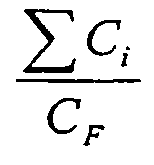
Anschließend steuert die Kalibriereinheit 21 über die Steuerleitung 24 (nicht dargestellt), Schalter derart an, dass das zugeführte digitale Zufallssignal sukzessive oder zufällig bzw. in einer beliebigen Reihenfolge an die verschiedenen DAC-Kondensatoren 25-1 bis 25-4 geschaltet wird. In gleicher Weise berechnet anschließend die Kalibriereinheit 21 die verschiedenen Signalverstärkungen V1, V2, V3, V4. Die berechneten fünf Signalverstärkungen VKal (CKal), V1 (C1), V2 (C2), V3 (C3), V4 (C4) werden in Register der Kalibriereinheit 21 zwischengespeichert. Die Kalibriereinheit 21 berechnet anschließend aus den vier zwischengespeicherten Signalverstärkungen V1, V2, V3, V4 der DAC-Kondensatoren 25-1, 25-2, 25-3, 25-4 einen Mittelwert V = (V1 + V2 + V3 + V4) : 4 und gibt diesen ermittelten Verstärkungsfaktor als Multiplikator über die Leitung 33 an die Gewichtungseinheit 9A der ersten Wandlerstufe A ab. Darüber hinaus berechnet die Kalibriereinheit 21 die Differenzen ΔVIJ zwischen den zwischengespeicherten Signalverstärkungen V, die den jeweiligen Umschaltfehler zwischen den unterschiedlichen DAC-Stufen entsprechen. Dieser DAC-Fehler bzw. DAC-Error beinhaltet auch das Einschalten der Kalibrierkapazität 31.Subsequently, the
Die von den Wandlerstufen abgegebenen, durch die Gewichtungseinheiten 9 gewichteten Ausgabewerte werden mittels Addierern 34 und Schiebegliedern 35 zu einem digitalen Ausgabewert des Analog/Digitalwandlers 1 summiert.The outputted by the weighting units 9 output from the converter stages output values are summed by means of adders 34 and slide members 35 to a digital output value of the analog /
Der von der Kalibriereinheit 21 berechnete DAC-Error wird über eine Leitung 36 einem Subtrahierer 37 zugeführt. Der berechnete Umschaltfehler bzw. DAC-Error wird durch den Subtrahierer 37 von dem ermittelten digitalen Ausgabewert der Wandlerstufen zur Fehlerkompensation abgezogen.The DAC error calculated by the
Die durchgeführte Kalibrierung erfolgt bei dem erfindungsgemäßen Analog/Digitalwandler 1 ständig im Hintergrund (Background-Kalibration). Mit dem erfindungsgemäßen Analog/Digitalwandler 1 werden sowohl Signalverstärkungsfehler als auch Umschaltfehler bzw. DAC-Fehler ausgeglichen. Die Fehler werden dabei kontinuierlich digital berechnet. Ein aufwendiges Trimmen ist nicht mehr erforderlich. Auch die Drift bei der Umgebungstemperatur und der Versorgungsspannung wird dabei kontinuierlich ausgeglichen. Mit Ausnahme der zusätzlich notwendigen Kalibrierkapazität 31 kann die Implementierung der Kalibrierung vollständig digital erfolgen.The calibration carried out in the analog /
Bei dem erfindungsgemäßen Kalibriervorgang wird zur Bestimmung der Kapazität eines DAC-Kondensators und zur Bestimmung der zugehörigen Verstärkung des DAC-Kondensators diese Kapazität gegen die Kapazität des Kalibrierkondensators ausgetauscht. Aus dem Gewicht kann die Gesamtverstärkung und der Stufenunterschied berechnet werden und im digitalen Bereich eine Korrektur des berechneten digitalen Ausgabewertes vorgenommen werden. Die in den Wandlerstufen vorgesehenen Digital/Analogwandler 13 sind vorzugsweise vollständig differentiell aufgebaut und weisen eine hohe Auflösung auf. Die Auflösung kann beispielsweise 4,5 Bit betragen.
Die in Figur 4 dargestellte Kalibriereinheit 21 kann für jede Wandlerstufe separat vorgesehen werden. Bei einer bevorzugten Ausführungsform ist nur eine Kalibriereinheit 21 vorgesehen, die mittels eines Multiplexers an die unterschiedlichen Wandlerstufen schaltbar ist.In the calibration process according to the invention, this capacitance is exchanged for the capacitance of the calibration capacitor to determine the capacitance of a DAC capacitor and to determine the associated gain of the DAC capacitor. From the weight, the overall gain and the Step difference are calculated and in the digital domain, a correction of the calculated digital output value are made. The provided in the converter stages digital / analog converter 13 are preferably completely differentially constructed and have a high resolution. The resolution can be 4.5 bits, for example.
The
- 11
- SA-WandlerSA Converters
- 22
- S/H-StufeS / H stage
- 33
- Komparatorcomparator
- 44
- digitale Steuerung (Gewichtungseinheit)digital control (weighting unit)
- 55
- D/A-WandlerD / A converter
- 66
- Ausgangoutput
- 1010
- Pipeline-WandlerPipeline converter
- 1111
- S/H-StufeS / H stage
- 1212
- Verstärkeramplifier
- 1313
- Komparatorcomparator
- 1414
- Subtrahierknotensubtracting node
- 1515
- Speichergliedmemory element
- 1616
- Addierknotenadding node
- 1717
- Addierknotenadding node
- 1818
- digitales Zufallssignaldigital random signal
- 1919
- D/A-WandlerD / A converter
- 2020
- digitale Gewichtungseinheitdigital weighting unit
- 2121
- Subtrahierknotensubtracting node
- 2222
- Korrelationseinheitcorrelation unit
- 2424
- Signalpfadsignal path
- 2525
- Auswerteeinheitevaluation
- 2626
- Differenzsignaldifference signal
- 2727
- Filterfilter
- 2828
- Kalibriereinrichtungcalibration
- 2929
- Kalibrierpfadcalibration path
- ainain
- analoges Eingangssignalanalog input signal
- REFREF
- Referenzgrößereference size
Claims (14)
- A/D converter, for converting an analog input signal (ain) into a digital output value, having:(a) at least one converter stage which respectively has:(a1) a sample & hold circuit (3) for sampling the analog input signal (ain),(a2) a comparator unit (5) which compares the input signal with a reference value (REF) in order to produce a digital output value from the converter stage,(a3) a digital/analog converter (13) for converting the digital output value into an analog signal,(a4) a subtractor (11) for subtracting the analog signal which is output by the digital/analog converter (13) from the sampled input signal, and(a5) a signal amplifier (17) for amplifying the output signal which is output by the subtractor (11) with a particular signal gain factor (V) for the next converter stage, and(a6) a weighting unit (9) for multiplying the digital output value by a multiplier for addition to further weighted output values from converter stages to produce the digital output value from the analog/digital converter (1);(b) a random signal generator (19) for generating a random signal which is fed into the converter stage;(c) characterized in that: it contains at least one calibration unit (21) which respectively has:(c1) a calibration amplifier with an adjustable calibration gain factor for signal amplification for the random signal, (c2) an evaluation unit which correlates the random signal which is fed into the signal path and is amplified by the converter stage with the random signal amplified by the calibration amplifier in the calibration unit (21), in order to generate a setting signal for setting the calibration gain factor, such that the output signal from the evaluation unit is at a minimum and hence the calculated calibration gain factor corresponds to the gain (V) which is brought about by the digital/analog converter (13) and the signal amplifier (17) in the converter stage;(d) where the random generator (19) applies the random signal, via a switch which can be controlled by the calibration unit (21), to a calibration capacitor (31) within the digital/analog converter (13) in the converter stage in order to feed it into the signal path;(e) where the random signal can be connected to further DAC capacitors (25) within the digital/analog converter (13) in order to calculate the respective signal gains of the DAC stages in the digital/analog converter (13), and where the calibration unit (21) uses the ascertained signal gains (Vi) of the DAC stages in the digital/analog converter (13) to calculate the signal gain differences ΔVij between the DAC stages in order to calculate a transfer error (DAC error) for the digital/analog converter (13).
- Analog/digital converter according to claim 1,
characterized
in that the calculated transfer error (DAC error) is deducted from the digital output value from the converter stages using a subtractor (37) in order to compensate for errors. - Analog/digital converter according to claim 1 or 2,
characterized
in that the calculated signal gains (Vi) are buffer-stored in registers in the calibration unit (21). - Analog/digital converter according to claim 3,
characterized
in that the calibration unit (21) calculates a mean value between stored signal gains. - Analog/digital converter according to claim 4,
characterized
in that the calculated mean value for the signal gains is applied as a multiplier to the weighting unit (9) in the converter stage by the calibration unit (21). - Analog/digital converter according to one of the preceding claims,
characterized
in that the calibration amplifier in the calibration unit (21) has a subtraction circuit connected downstream of it which subtracts the signal amplified by the calibration amplifier from a signal derived from the signal path in the converter stages and outputs a difference signal to the evaluation unit. - Analog/digital converter according to claim 6,
characterized
in that the evaluation unit cross-correlates the difference signal with the digital random signal. - Analog/digital converter according to claim 7,
characterized
in that the evaluation unit has a filter connected downstream of it. - Analog/digital converter according to claim 1,
characterized
in that the calibration unit (21) has a flow controller for generating control signals for actuating switches. - Analog/digital converter according to claim 1,
characterized
in that the output values from the comparator units (5) are thermometer-coded. - Analog/digital converter according to claim 1,
characterized
in that at least two converter stages are provided. - Analog/digital converter according to claim 1,
characterized
in that the random signal is a digital random signal (PSR). - Analog/digital converter according to claim 1,
characterized
in that the analog/digital converters (1) are of fully differential design. - Analog/digital converter according to claim 1,
characterized
in that the digital/analog converter (13) has a calibration capacitor (31) via which the random signal is fed into the signal path.
Applications Claiming Priority (3)
| Application Number | Priority Date | Filing Date | Title |
|---|---|---|---|
| DE10255354A DE10255354B3 (en) | 2002-11-27 | 2002-11-27 | Analogue/digital converter with incorporated calibration unit used for determining digital/analogue error of digital/analogue converter |
| DE10255354 | 2002-11-27 | ||
| PCT/EP2003/011468 WO2004054111A2 (en) | 2002-11-27 | 2003-10-16 | A/d converter with minimized switching error |
Publications (2)
| Publication Number | Publication Date |
|---|---|
| EP1568138A2 EP1568138A2 (en) | 2005-08-31 |
| EP1568138B1 true EP1568138B1 (en) | 2007-03-07 |
Family
ID=31197640
Family Applications (1)
| Application Number | Title | Priority Date | Filing Date |
|---|---|---|---|
| EP03785625A Expired - Fee Related EP1568138B1 (en) | 2002-11-27 | 2003-10-16 | A/d converter with minimized switching error |
Country Status (5)
| Country | Link |
|---|---|
| US (1) | US7095346B2 (en) |
| EP (1) | EP1568138B1 (en) |
| CN (1) | CN100472965C (en) |
| DE (2) | DE10255354B3 (en) |
| WO (1) | WO2004054111A2 (en) |
Families Citing this family (34)
| Publication number | Priority date | Publication date | Assignee | Title |
|---|---|---|---|---|
| DE10344354B4 (en) * | 2003-09-24 | 2006-11-02 | Infineon Technologies Ag | Analog-to-digital converter and method for operating an analog-to-digital converter |
| CN100512016C (en) * | 2004-02-10 | 2009-07-08 | 三洋电机株式会社 | Analog-digital converter |
| JP2005249690A (en) * | 2004-03-05 | 2005-09-15 | Agilent Technol Inc | Signal-retaining method, analog-to-digital conversion method, signal-retaining device, analog-to-digital converting device, and signal observing device |
| JP3785175B2 (en) * | 2004-03-30 | 2006-06-14 | 株式会社東芝 | Multi-input A / D converter and radio receiver using the same |
| DE102005015807B3 (en) * | 2005-04-06 | 2006-10-12 | Infineon Technologies Ag | Analog to digital converter e.g. pipeline converter, has concatenation device to concatenate total weighted correction value and doubled digital output value to provide corrected output value, and condenser unit have unit condensers |
| JP4690105B2 (en) * | 2005-04-26 | 2011-06-01 | パナソニック株式会社 | Successive approximation type A / D converter |
| CN1945978B (en) * | 2005-05-27 | 2012-01-18 | 阿纳洛格装置公司 | Pipeline ADC employing integral non-linear error correction |
| US7486215B1 (en) * | 2006-08-30 | 2009-02-03 | Marvell International Ltd. | Apparatus, method, and circuit for baseline loop analog cancellation |
| JP4480744B2 (en) * | 2007-07-31 | 2010-06-16 | 三洋電機株式会社 | Analog to digital converter |
| US7535391B1 (en) * | 2008-01-07 | 2009-05-19 | Freescale Semiconductor, Inc. | Analog-to-digital converter having random capacitor assignment and method thereof |
| CN101247127B (en) * | 2008-03-27 | 2010-04-21 | 凌阳多媒体股份有限公司 | Switching type capacitor D/A converter |
| JP2009246752A (en) * | 2008-03-31 | 2009-10-22 | Panasonic Corp | Pipeline a/d converter |
| WO2010041187A1 (en) * | 2008-10-06 | 2010-04-15 | Nxp B.V. | A method of gain calibration of an adc stage and an adc stage |
| CN101854174B (en) * | 2010-05-18 | 2012-04-18 | 上海萌芯电子科技有限公司 | Streamline analog-digital converter and sub conversion stage circuit thereof |
| US8451152B2 (en) * | 2011-02-22 | 2013-05-28 | Texas Instruments Incorporated | Pipelined ADC inter-stage error calibration |
| US8441380B2 (en) * | 2011-05-20 | 2013-05-14 | Texas Instruments Incorporated | Method and apparatus for performing data conversion with non-uniform quantization |
| US8581769B2 (en) * | 2011-11-22 | 2013-11-12 | Stmicroelectronics International N.V. | Multiplying digital-to-analog converter configured to maintain impedance balancing |
| US8791845B2 (en) * | 2012-08-31 | 2014-07-29 | Texas Instruments Incorporated | Circuitry and method for reducing area and power of a pipelince ADC |
| US8698666B1 (en) * | 2012-10-01 | 2014-04-15 | Omnivision Technologies, Inc. | Random estimation analog-to-digital converter |
| US9041569B2 (en) * | 2013-06-28 | 2015-05-26 | Silicon Laboratories Inc. | Method and apparatus for calibration of successive approximation register analog-to-digital converters |
| US9680309B2 (en) * | 2013-11-21 | 2017-06-13 | Active-Semi, Inc. | Auto load switch detection for wireless power receiver |
| US9124286B1 (en) * | 2014-02-18 | 2015-09-01 | Integrated Device Technology, Inc. | Protection for analog to digital converters |
| CN105897265B (en) * | 2014-12-12 | 2020-08-21 | 恩智浦美国有限公司 | Analog-to-digital converter with controlled error calibration |
| US10056914B2 (en) * | 2015-12-18 | 2018-08-21 | Analog Devices Global | Frequency-domain ADC flash calibration |
| TWI594579B (en) * | 2016-06-13 | 2017-08-01 | 瑞昱半導體股份有限公司 | Successive approximation register analog to digital converter and analog to digital conversion method thereof |
| US9734703B1 (en) * | 2016-06-23 | 2017-08-15 | Nxp B.V. | Sensor apparatuses and methods |
| US10311962B2 (en) * | 2017-02-23 | 2019-06-04 | Mediatek Inc. | Differential sampling circuit |
| CN107579740B (en) * | 2017-08-25 | 2020-12-08 | 深圳清华大学研究院 | Method for improving output precision of pipeline analog-to-digital converter and analog-to-digital converter |
| US10437514B2 (en) * | 2017-10-02 | 2019-10-08 | Micron Technology, Inc. | Apparatuses and methods including memory commands for semiconductor memories |
| US10555269B2 (en) * | 2017-11-24 | 2020-02-04 | Mediatek Inc. | Amplifier circuit having controllable output stage |
| US10382050B1 (en) * | 2018-05-25 | 2019-08-13 | Dialog Semiconductor (Uk) Limited | Integrated multiplying successive approximation analog to digital converter |
| CN109194331B (en) * | 2018-08-29 | 2021-10-26 | 苏州瑞迈斯医疗科技有限公司 | Electronic device and method for correcting comparator in electronic device |
| US10541699B1 (en) * | 2018-10-11 | 2020-01-21 | Nxp B.V. | Signal processing and conversion |
| CN111147077B (en) * | 2018-11-05 | 2023-08-11 | 瑞昱半导体股份有限公司 | Gain calibration device and method for residual amplifier of analog-digital converter |
Family Cites Families (10)
| Publication number | Priority date | Publication date | Assignee | Title |
|---|---|---|---|---|
| US4399426A (en) * | 1981-05-04 | 1983-08-16 | Tan Khen Sang | On board self-calibration of analog-to-digital and digital-to-analog converters |
| US4996530A (en) * | 1989-11-27 | 1991-02-26 | Hewlett-Packard Company | Statistically based continuous autocalibration method and apparatus |
| US5187481A (en) * | 1990-10-05 | 1993-02-16 | Hewlett-Packard Company | Combined and simplified multiplexing and dithered analog to digital converter |
| US5929796A (en) * | 1997-04-29 | 1999-07-27 | National Semiconductor Corporation | Self-calibrating reversible pipeline analog to digital and digital to analog converter |
| US5861828A (en) * | 1997-10-14 | 1999-01-19 | National Semiconductor Corporation | Apparatus and method for monotonic digital calibration of a pipeline analog-to-digital converter |
| US6191715B1 (en) * | 1998-10-29 | 2001-02-20 | Burr-Brown Corporation | System for calibration of a digital-to-analog converter |
| US6400302B1 (en) * | 2001-02-26 | 2002-06-04 | Analog Devices, Inc. | Quasi-differential successive-approximation structures and methods for converting analog signals into corresponding digital signals |
| DE10133538B4 (en) * | 2001-07-11 | 2004-02-19 | Infineon Technologies Ag | Calibration device for the calibration of A / D converters with any bit weight |
| US6603416B2 (en) * | 2001-10-01 | 2003-08-05 | International Business Machines Corporation | Method and circuit for dynamic calibration of flash analog to digital converters |
| US6784824B1 (en) * | 2002-08-29 | 2004-08-31 | Xilinx, Inc. | Analog-to-digital converter which is substantially independent of capacitor mismatch |
-
2002
- 2002-11-27 DE DE10255354A patent/DE10255354B3/en not_active Expired - Fee Related
-
2003
- 2003-10-16 DE DE50306772T patent/DE50306772D1/en not_active Expired - Fee Related
- 2003-10-16 EP EP03785625A patent/EP1568138B1/en not_active Expired - Fee Related
- 2003-10-16 WO PCT/EP2003/011468 patent/WO2004054111A2/en active IP Right Grant
- 2003-10-16 CN CNB2003801004048A patent/CN100472965C/en not_active Expired - Fee Related
-
2004
- 2004-10-26 US US10/973,656 patent/US7095346B2/en active Active
Also Published As
| Publication number | Publication date |
|---|---|
| WO2004054111A2 (en) | 2004-06-24 |
| EP1568138A2 (en) | 2005-08-31 |
| WO2004054111A3 (en) | 2004-08-12 |
| US7095346B2 (en) | 2006-08-22 |
| CN1692555A (en) | 2005-11-02 |
| DE10255354B3 (en) | 2004-03-04 |
| US20050116846A1 (en) | 2005-06-02 |
| DE50306772D1 (en) | 2007-04-19 |
| CN100472965C (en) | 2009-03-25 |
Similar Documents
| Publication | Publication Date | Title |
|---|---|---|
| EP1568138B1 (en) | A/d converter with minimized switching error | |
| DE102017102501B4 (en) | Dual conversion ADC background calibration | |
| DE102009005770B4 (en) | SAR ADC and methods with INL compensation | |
| DE102009010155B4 (en) | Digital trimming of (SAR) ADCs | |
| DE60029584T2 (en) | CORRECTION OF STATIC ERRORS IN AN A / D CONVERTER | |
| DE102011110115B4 (en) | Apparatus and method for measuring the DNL of a SAR ADC | |
| DE19830796C2 (en) | Analog / digital converter circuit | |
| DE102015107885A1 (en) | Error measurement and calibration of analog-to-digital converters | |
| DE3642070A1 (en) | METHOD FOR MATCHING A NUMBER OF CAPACITIES IN A MONOLITICAL INTEGRATED CIRCUIT | |
| DE60123535T2 (en) | Multi-stage converter with application of a digital dither signal | |
| DE112016003065T5 (en) | Gain calibration for AD converter with external reference | |
| DE19924075A1 (en) | Algorithmic analogue to digital converter for high speed operation | |
| DE102019112542A1 (en) | RESERVOIR CONDENSER-BASED ANALOG DIGITAL CONVERTER | |
| DE102011006760B4 (en) | A / D converter device and signal processing unit hereby | |
| DE19936327A1 (en) | Analog / digital or digital / analog converter | |
| DE60309025T2 (en) | offset calibration | |
| DE102017102091A1 (en) | SAR ADC performance optimization with dynamic bit-test settings | |
| DE10314189A1 (en) | Calibration method for analog-to-digital or digital-to-analog converter, by using fixed values for ratios between weighting values and solving equations | |
| DE102013105127B4 (en) | Background technologies for calibrating comparators | |
| EP0349793A2 (en) | Circuit arrangement for analog-to-digital conversion | |
| DE102014117457A1 (en) | STOCHASTIC CODING IN ANALOG-DIGITAL IMPLEMENTATION | |
| EP0444234B1 (en) | Method and device for analogue/digital conversion | |
| EP0444233A1 (en) | Method and device for the analogue/digital conversion of a time-variant analogue input signal | |
| DE10133538B4 (en) | Calibration device for the calibration of A / D converters with any bit weight | |
| DE4009383C2 (en) |
Legal Events
| Date | Code | Title | Description |
|---|---|---|---|
| PUAI | Public reference made under article 153(3) epc to a published international application that has entered the european phase |
Free format text: ORIGINAL CODE: 0009012 |
|
| 17P | Request for examination filed |
Effective date: 20040903 |
|
| AK | Designated contracting states |
Kind code of ref document: A2 Designated state(s): AT BE BG CH CY CZ DE DK EE ES FI FR GB GR HU IE IT LI LU MC NL PT RO SE SI SK TR |
|
| RBV | Designated contracting states (corrected) |
Designated state(s): DE FR GB |
|
| GRAP | Despatch of communication of intention to grant a patent |
Free format text: ORIGINAL CODE: EPIDOSNIGR1 |
|
| RIC1 | Information provided on ipc code assigned before grant |
Ipc: H03M 1/10 20060101AFI20060825BHEP |
|
| GRAS | Grant fee paid |
Free format text: ORIGINAL CODE: EPIDOSNIGR3 |
|
| GRAA | (expected) grant |
Free format text: ORIGINAL CODE: 0009210 |
|
| AK | Designated contracting states |
Kind code of ref document: B1 Designated state(s): DE FR GB |
|
| REG | Reference to a national code |
Ref country code: GB Ref legal event code: FG4D Free format text: NOT ENGLISH |
|
| REF | Corresponds to: |
Ref document number: 50306772 Country of ref document: DE Date of ref document: 20070419 Kind code of ref document: P |
|
| GBT | Gb: translation of ep patent filed (gb section 77(6)(a)/1977) |
Effective date: 20070524 |
|
| ET | Fr: translation filed | ||
| PLBE | No opposition filed within time limit |
Free format text: ORIGINAL CODE: 0009261 |
|
| STAA | Information on the status of an ep patent application or granted ep patent |
Free format text: STATUS: NO OPPOSITION FILED WITHIN TIME LIMIT |
|
| 26N | No opposition filed |
Effective date: 20071210 |
|
| PGFP | Annual fee paid to national office [announced via postgrant information from national office to epo] |
Ref country code: GB Payment date: 20071023 Year of fee payment: 5 Ref country code: FR Payment date: 20071016 Year of fee payment: 5 |
|
| PGFP | Annual fee paid to national office [announced via postgrant information from national office to epo] |
Ref country code: DE Payment date: 20071211 Year of fee payment: 5 |
|
| GBPC | Gb: european patent ceased through non-payment of renewal fee |
Effective date: 20081016 |
|
| REG | Reference to a national code |
Ref country code: FR Ref legal event code: ST Effective date: 20090630 |
|
| PG25 | Lapsed in a contracting state [announced via postgrant information from national office to epo] |
Ref country code: DE Free format text: LAPSE BECAUSE OF NON-PAYMENT OF DUE FEES Effective date: 20090501 |
|
| PG25 | Lapsed in a contracting state [announced via postgrant information from national office to epo] |
Ref country code: FR Free format text: LAPSE BECAUSE OF NON-PAYMENT OF DUE FEES Effective date: 20081031 |
|
| PG25 | Lapsed in a contracting state [announced via postgrant information from national office to epo] |
Ref country code: GB Free format text: LAPSE BECAUSE OF NON-PAYMENT OF DUE FEES Effective date: 20081016 |