EP1566841A1 - Solid-state imaging device and radiation imaging system - Google Patents
Solid-state imaging device and radiation imaging system Download PDFInfo
- Publication number
- EP1566841A1 EP1566841A1 EP03811936A EP03811936A EP1566841A1 EP 1566841 A1 EP1566841 A1 EP 1566841A1 EP 03811936 A EP03811936 A EP 03811936A EP 03811936 A EP03811936 A EP 03811936A EP 1566841 A1 EP1566841 A1 EP 1566841A1
- Authority
- EP
- European Patent Office
- Prior art keywords
- semiconductor substrate
- imaging apparatus
- solid
- conductivity type
- electroconductive member
- Prior art date
- Legal status (The legal status is an assumption and is not a legal conclusion. Google has not performed a legal analysis and makes no representation as to the accuracy of the status listed.)
- Granted
Links
Images




Classifications
-
- H—ELECTRICITY
- H10—SEMICONDUCTOR DEVICES; ELECTRIC SOLID-STATE DEVICES NOT OTHERWISE PROVIDED FOR
- H10F—INORGANIC SEMICONDUCTOR DEVICES SENSITIVE TO INFRARED RADIATION, LIGHT, ELECTROMAGNETIC RADIATION OF SHORTER WAVELENGTH OR CORPUSCULAR RADIATION
- H10F39/00—Integrated devices, or assemblies of multiple devices, comprising at least one element covered by group H10F30/00, e.g. radiation detectors comprising photodiode arrays
- H10F39/10—Integrated devices
- H10F39/12—Image sensors
- H10F39/18—Complementary metal-oxide-semiconductor [CMOS] image sensors; Photodiode array image sensors
- H10F39/189—X-ray, gamma-ray or corpuscular radiation imagers
- H10F39/1898—Indirect radiation image sensors, e.g. using luminescent members
-
- H—ELECTRICITY
- H10—SEMICONDUCTOR DEVICES; ELECTRIC SOLID-STATE DEVICES NOT OTHERWISE PROVIDED FOR
- H10F—INORGANIC SEMICONDUCTOR DEVICES SENSITIVE TO INFRARED RADIATION, LIGHT, ELECTROMAGNETIC RADIATION OF SHORTER WAVELENGTH OR CORPUSCULAR RADIATION
- H10F30/00—Individual radiation-sensitive semiconductor devices in which radiation controls the flow of current through the devices, e.g. photodetectors
- H10F30/20—Individual radiation-sensitive semiconductor devices in which radiation controls the flow of current through the devices, e.g. photodetectors the devices having potential barriers, e.g. phototransistors
-
- H—ELECTRICITY
- H10—SEMICONDUCTOR DEVICES; ELECTRIC SOLID-STATE DEVICES NOT OTHERWISE PROVIDED FOR
- H10F—INORGANIC SEMICONDUCTOR DEVICES SENSITIVE TO INFRARED RADIATION, LIGHT, ELECTROMAGNETIC RADIATION OF SHORTER WAVELENGTH OR CORPUSCULAR RADIATION
- H10F39/00—Integrated devices, or assemblies of multiple devices, comprising at least one element covered by group H10F30/00, e.g. radiation detectors comprising photodiode arrays
- H10F39/80—Constructional details of image sensors
- H10F39/807—Pixel isolation structures
-
- H—ELECTRICITY
- H04—ELECTRIC COMMUNICATION TECHNIQUE
- H04N—PICTORIAL COMMUNICATION, e.g. TELEVISION
- H04N25/00—Circuitry of solid-state image sensors [SSIS]; Control thereof
- H04N25/30—Circuitry of solid-state image sensors [SSIS]; Control thereof for transforming X-rays into image signals
Definitions
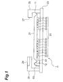
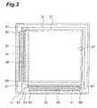
- the photosensitive section 31 includes the isolation region 12e formed between adjacent n + -type semiconductor regions 12d, and the metal wire 14 is electrically connected to the isolation region 12e. This can achieve commonality between the electroconductive member for discharging the charge generated in the region except for the photodiodes 33, to the outside, and the electroconductive member for grounding the isolation region 12e, thereby preventing complexity of structure.
Landscapes
- Solid State Image Pick-Up Elements (AREA)
- Measurement Of Radiation (AREA)
- Transforming Light Signals Into Electric Signals (AREA)
- Light Receiving Elements (AREA)
Abstract
Description
Claims (11)
- A solid-state imaging apparatus comprising:wherein the electroconductive member is connected to a fixed potential, or is grounded.a photosensitive section comprising a semiconductor substrate of a first conductivity type, and a plurality of second conductivity type semiconductor regions arrayed in a two-dimensional pattern on one side of the semiconductor substrate, wherein the semiconductor substrate and each second conductivity type semiconductor region constitute a pn junction to function as a photodiode; andan electroconductive member provided so as to cover at least the pn junction portions exposed on the one side of the semiconductor substrate,
- The solid-state imaging apparatus according to Claim 1, wherein the electroconductive member is of grid shape when viewed from a direction of incidence of light to the photosensitive section, and is provided so as to cover the pn junction portions exposed on the one side of the semiconductor substrate and portions between the second conductivity type semiconductor regions adjacent to each other.
- The solid-state imaging apparatus according to Claim 1, wherein the photosensitive section further comprises an isolation region formed between the second conductivity type semiconductor regions adjacent to each other, and
wherein the electroconductive member is electrically connected to the isolation region. - The solid-state imaging apparatus according to Claim 1, further comprising:wherein the wires are located above the electroconductive member.signal lines for readout of outputs from the photodiodes, which are electrically connected to the photodiodes;a switch group consisting of a plurality of switches for controlling electrical connection and disconnection between each photodiode and the signal line in each column of the photodiodes; andwires connected to control terminals of the respective switches forming the switch group, and arranged to supply a scan signal to turn each switch off or on in each row of the photodiodes, to the control terminals,
- A solid-state imaging apparatus comprising:wherein the electroconductive member is connected to a fixed potential, or is grounded.a photosensitive section comprising a semiconductor substrate of a first conductivity type, and a plurality of second conductivity type semiconductor regions arrayed in a matrix of M rows and N columns on one side of the semiconductor substrate, wherein the semiconductor substrate and each second conductivity type semiconductor region constitute a pn junction to function as a photodiode;first wires provided in the respective columns;a first switch group consisting of a plurality of switches for connection between each photodiode and the first wire in each column;a vertical shift register for outputting a vertical scan signal to open and close each switch forming the first switch group, in each row;second wires for connecting control terminals of the respective switches forming the first switch group, to the vertical shift register in each row;a second switch group consisting of a plurality of switches for connection between each first wire and a signal output line;a horizontal shift register for outputting a horizontal scan signal to open and close each switch forming the second switch group, in each column; andan electroconductive member provided so as to cover at least the pn junction portions exposed on the one side of the semiconductor substrate,
- The solid-state imaging apparatus according to Claim 5, wherein the electroconductive member is of grid shape when viewed from a direction of incidence of light to the photosensitive section, and is provided so as to cover the pn junction portions exposed on the one side of the semiconductor substrate and portions between the second conductivity type semiconductor regions adjacent to each other.
- The solid-state imaging apparatus according to Claim 5, wherein the photosensitive section further comprises an isolation region formed between the second conductivity type semiconductor regions adjacent to each other, and
wherein the electroconductive member is electrically connected to the isolation region. - The solid-state imaging apparatus according to Claim 5, wherein the second wires are located above the electroconductive member.
- A solid-state imaging apparatus comprising:a photosensitive section comprising a semiconductor substrate of a first conductivity type, and a plurality of second conductivity type semiconductor regions arrayed in a two-dimensional pattern on one side of the semiconductor substrate, wherein the semiconductor substrate and each second conductivity type semiconductor region constitute a pn junction to function as a photodiode; andan electroconductive member for discharging a charge generated in a region except for the photodiodes, to the outside.
- The solid-state imaging apparatus according to Claim 9, wherein the electroconductive member is provided above the pn junction portions so as to cover at least the pn junction portions exposed on the one side of the semiconductor substrate, and is connected to a fixed potential, or is grounded.
- A radiographic imaging apparatus comprising:the solid-state imaging apparatus as set forth in any one of Claims 1 to 10; anda scintillator for converting radiation to visible light, which is provided so as to cover the plurality of photodiodes.
Applications Claiming Priority (3)
| Application Number | Priority Date | Filing Date | Title |
|---|---|---|---|
| JP2002346262 | 2002-11-28 | ||
| JP2002346262A JP4391079B2 (en) | 2002-11-28 | 2002-11-28 | Solid-state imaging device and radiation imaging device |
| PCT/JP2003/015109 WO2004049448A1 (en) | 2002-11-28 | 2003-11-26 | Solid-state imaging device and radiation imaging system |
Publications (3)
| Publication Number | Publication Date |
|---|---|
| EP1566841A1 true EP1566841A1 (en) | 2005-08-24 |
| EP1566841A4 EP1566841A4 (en) | 2007-11-28 |
| EP1566841B1 EP1566841B1 (en) | 2013-01-02 |
Family
ID=32376052
Family Applications (1)
| Application Number | Title | Priority Date | Filing Date |
|---|---|---|---|
| EP03811936A Expired - Lifetime EP1566841B1 (en) | 2002-11-28 | 2003-11-26 | Solid-state imaging device and radiation imaging system |
Country Status (6)
| Country | Link |
|---|---|
| US (1) | US7372037B2 (en) |
| EP (1) | EP1566841B1 (en) |
| JP (1) | JP4391079B2 (en) |
| CN (1) | CN100442528C (en) |
| AU (1) | AU2003302295A1 (en) |
| WO (1) | WO2004049448A1 (en) |
Cited By (1)
| Publication number | Priority date | Publication date | Assignee | Title |
|---|---|---|---|---|
| RU2351038C2 (en) * | 2005-08-31 | 2009-03-27 | Кэнон Кабусики Кайся | Radiation detector, radiation image generating apparatus and system for generating radiation images |
Families Citing this family (8)
| Publication number | Priority date | Publication date | Assignee | Title |
|---|---|---|---|---|
| JP4270455B2 (en) * | 2004-03-26 | 2009-06-03 | 富士フイルム株式会社 | Solid-state imaging device |
| US7554031B2 (en) * | 2005-03-03 | 2009-06-30 | Sunpower Corporation | Preventing harmful polarization of solar cells |
| JP4634209B2 (en) * | 2005-04-14 | 2011-02-16 | 浜松ホトニクス株式会社 | Electronic detector |
| US7259377B2 (en) * | 2005-12-15 | 2007-08-21 | General Electric Company | Diode design to reduce the effects of radiation damage |
| US8426902B2 (en) * | 2010-07-30 | 2013-04-23 | Unisantis Electronics Singapore Pte Ltd. | Solid-state imaging device |
| US9917118B2 (en) * | 2011-09-09 | 2018-03-13 | Zecotek Imaging Systems Pte. Ltd. | Photodetector array and method of manufacture |
| CN103633033B (en) * | 2012-08-23 | 2018-04-20 | 鸿富锦精密工业(深圳)有限公司 | Image Sensor module and taken module |
| JP6576064B2 (en) * | 2015-03-18 | 2019-09-18 | キヤノン株式会社 | Radiation detection apparatus, radiation imaging system, and method of manufacturing radiation detection apparatus |
Family Cites Families (16)
| Publication number | Priority date | Publication date | Assignee | Title |
|---|---|---|---|---|
| JPS61141177A (en) * | 1984-12-14 | 1986-06-28 | Hamamatsu Photonics Kk | Semiconductor photodetecting device |
| JPH0695571B2 (en) * | 1985-10-12 | 1994-11-24 | 新技術事業団 | Photoelectric conversion device |
| JP2757624B2 (en) * | 1991-10-21 | 1998-05-25 | 日本電気株式会社 | Infrared solid-state imaging device and method of manufacturing the same |
| JP3486490B2 (en) | 1995-09-04 | 2004-01-13 | キヤノン株式会社 | Radiation detector |
| CA2261663C (en) * | 1997-02-14 | 2001-08-28 | Hamamatsu Photonics K.K. | Radiation detection device and method of producing the same |
| JPH11122533A (en) * | 1997-10-17 | 1999-04-30 | Sharp Corp | Semiconductor amplifier circuit and solid-state imaging device using the same |
| CA2241779C (en) * | 1998-06-26 | 2010-02-09 | Ftni Inc. | Indirect x-ray image detector for radiology |
| JP4005704B2 (en) | 1998-07-14 | 2007-11-14 | 浜松ホトニクス株式会社 | X-ray panel sensor |
| JP4812940B2 (en) * | 1998-10-30 | 2011-11-09 | 浜松ホトニクス株式会社 | Solid-state imaging device array |
| US6350663B1 (en) | 2000-03-03 | 2002-02-26 | Agilent Technologies, Inc. | Method for reducing leakage currents of active area diodes and source/drain diffusions |
| CN1324714C (en) * | 2000-04-04 | 2007-07-04 | 浜松光子学株式会社 | Semiconductor energy beam detection element |
| TW449939B (en) * | 2000-07-03 | 2001-08-11 | United Microelectronics Corp | Photodiode structure |
| US6717151B2 (en) * | 2000-07-10 | 2004-04-06 | Canon Kabushiki Kaisha | Image pickup apparatus |
| JP2002237614A (en) * | 2000-11-28 | 2002-08-23 | Canon Inc | Photoelectric conversion device, driving method thereof, and information processing device |
| JP2002252341A (en) | 2001-02-23 | 2002-09-06 | Fuji Film Microdevices Co Ltd | Solid-state imaging device |
| US6847039B2 (en) * | 2001-03-28 | 2005-01-25 | Canon Kabushiki Kaisha | Photodetecting device, radiation detecting device, and radiation imaging system |
-
2002
- 2002-11-28 JP JP2002346262A patent/JP4391079B2/en not_active Expired - Fee Related
-
2003
- 2003-11-26 WO PCT/JP2003/015109 patent/WO2004049448A1/en not_active Ceased
- 2003-11-26 EP EP03811936A patent/EP1566841B1/en not_active Expired - Lifetime
- 2003-11-26 US US10/536,904 patent/US7372037B2/en not_active Expired - Lifetime
- 2003-11-26 CN CNB2003801046214A patent/CN100442528C/en not_active Expired - Lifetime
- 2003-11-26 AU AU2003302295A patent/AU2003302295A1/en not_active Abandoned
Cited By (1)
| Publication number | Priority date | Publication date | Assignee | Title |
|---|---|---|---|---|
| RU2351038C2 (en) * | 2005-08-31 | 2009-03-27 | Кэнон Кабусики Кайся | Radiation detector, radiation image generating apparatus and system for generating radiation images |
Also Published As
| Publication number | Publication date |
|---|---|
| JP2004179539A (en) | 2004-06-24 |
| CN100442528C (en) | 2008-12-10 |
| US20060145084A1 (en) | 2006-07-06 |
| AU2003302295A1 (en) | 2004-06-18 |
| US7372037B2 (en) | 2008-05-13 |
| EP1566841A4 (en) | 2007-11-28 |
| JP4391079B2 (en) | 2009-12-24 |
| EP1566841B1 (en) | 2013-01-02 |
| WO2004049448A1 (en) | 2004-06-10 |
| CN1720620A (en) | 2006-01-11 |
Similar Documents
| Publication | Publication Date | Title |
|---|---|---|
| US7897930B2 (en) | Radiation imaging apparatus and radiation imaging system | |
| US20100054418A1 (en) | X-ray detecting element | |
| EP0964451B1 (en) | Photosensor and radiation detection system | |
| US7105829B2 (en) | Radiation detector having radiation sensitive semiconductor | |
| US7456880B2 (en) | Photoelectric conversion element having a plurality of semiconductor regions and including conductive layers provided on each isolation element region | |
| US7002155B2 (en) | X-ray imaging device | |
| EP0842541B1 (en) | Flat panel detector for radiation imaging with reduced trapped charges | |
| CA2233816A1 (en) | High resolution, low voltage flat-panel radiation imaging sensors | |
| US20090166545A1 (en) | Shielding an imaging array from x-ray noise | |
| US7372037B2 (en) | Solid-state imaging device and radiotion imaging system | |
| CN101390213B (en) | Radiation detector | |
| EP1566840B1 (en) | Solid-state imaging device and radiation imaging system | |
| US7432509B2 (en) | Radiographic imaging system | |
| JP2005203708A (en) | X-ray imaging device | |
| US7138637B2 (en) | X-ray imager | |
| JP2004177217A (en) | Radiation imaging apparatus |
Legal Events
| Date | Code | Title | Description |
|---|---|---|---|
| PUAI | Public reference made under article 153(3) epc to a published international application that has entered the european phase |
Free format text: ORIGINAL CODE: 0009012 |
|
| 17P | Request for examination filed |
Effective date: 20050602 |
|
| AK | Designated contracting states |
Kind code of ref document: A1 Designated state(s): AT BE BG CH CY CZ DE DK EE ES FI FR GB GR HU IE IT LI LU MC NL PT RO SE SI SK TR |
|
| AX | Request for extension of the european patent |
Extension state: AL LT LV MK |
|
| DAX | Request for extension of the european patent (deleted) | ||
| RBV | Designated contracting states (corrected) |
Designated state(s): CH DE FR GB IT LI |
|
| A4 | Supplementary search report drawn up and despatched |
Effective date: 20071031 |
|
| 17Q | First examination report despatched |
Effective date: 20071126 |
|
| GRAP | Despatch of communication of intention to grant a patent |
Free format text: ORIGINAL CODE: EPIDOSNIGR1 |
|
| GRAS | Grant fee paid |
Free format text: ORIGINAL CODE: EPIDOSNIGR3 |
|
| GRAA | (expected) grant |
Free format text: ORIGINAL CODE: 0009210 |
|
| AK | Designated contracting states |
Kind code of ref document: B1 Designated state(s): CH DE FR GB IT LI |
|
| REG | Reference to a national code |
Ref country code: GB Ref legal event code: FG4D |
|
| REG | Reference to a national code |
Ref country code: CH Ref legal event code: EP |
|
| REG | Reference to a national code |
Ref country code: DE Ref legal event code: R096 Ref document number: 60343034 Country of ref document: DE Effective date: 20130228 |
|
| PLBE | No opposition filed within time limit |
Free format text: ORIGINAL CODE: 0009261 |
|
| STAA | Information on the status of an ep patent application or granted ep patent |
Free format text: STATUS: NO OPPOSITION FILED WITHIN TIME LIMIT |
|
| 26N | No opposition filed |
Effective date: 20131003 |
|
| REG | Reference to a national code |
Ref country code: DE Ref legal event code: R097 Ref document number: 60343034 Country of ref document: DE Effective date: 20131003 |
|
| REG | Reference to a national code |
Ref country code: FR Ref legal event code: PLFP Year of fee payment: 13 |
|
| REG | Reference to a national code |
Ref country code: FR Ref legal event code: PLFP Year of fee payment: 14 |
|
| REG | Reference to a national code |
Ref country code: FR Ref legal event code: PLFP Year of fee payment: 15 |
|
| REG | Reference to a national code |
Ref country code: FR Ref legal event code: PLFP Year of fee payment: 16 |
|
| PGFP | Annual fee paid to national office [announced via postgrant information from national office to epo] |
Ref country code: FR Payment date: 20221010 Year of fee payment: 20 |
|
| PGFP | Annual fee paid to national office [announced via postgrant information from national office to epo] |
Ref country code: IT Payment date: 20221011 Year of fee payment: 20 Ref country code: GB Payment date: 20221006 Year of fee payment: 20 Ref country code: DE Payment date: 20221004 Year of fee payment: 20 |
|
| PGFP | Annual fee paid to national office [announced via postgrant information from national office to epo] |
Ref country code: CH Payment date: 20221103 Year of fee payment: 20 |
|
| P01 | Opt-out of the competence of the unified patent court (upc) registered |
Effective date: 20230517 |
|
| REG | Reference to a national code |
Ref country code: DE Ref legal event code: R071 Ref document number: 60343034 Country of ref document: DE |
|
| REG | Reference to a national code |
Ref country code: CH Ref legal event code: PL |
|
| REG | Reference to a national code |
Ref country code: GB Ref legal event code: PE20 Expiry date: 20231125 |
|
| PG25 | Lapsed in a contracting state [announced via postgrant information from national office to epo] |
Ref country code: GB Free format text: LAPSE BECAUSE OF EXPIRATION OF PROTECTION Effective date: 20231125 |
|
| PG25 | Lapsed in a contracting state [announced via postgrant information from national office to epo] |
Ref country code: GB Free format text: LAPSE BECAUSE OF EXPIRATION OF PROTECTION Effective date: 20231125 |