EP1566792A2 - Apparatus for driving plasma display panel - Google Patents
Apparatus for driving plasma display panel Download PDFInfo
- Publication number
- EP1566792A2 EP1566792A2 EP05002906A EP05002906A EP1566792A2 EP 1566792 A2 EP1566792 A2 EP 1566792A2 EP 05002906 A EP05002906 A EP 05002906A EP 05002906 A EP05002906 A EP 05002906A EP 1566792 A2 EP1566792 A2 EP 1566792A2
- Authority
- EP
- European Patent Office
- Prior art keywords
- data
- pulse
- electrode
- sustain
- phosphors
- Prior art date
- Legal status (The legal status is an assumption and is not a legal conclusion. Google has not performed a legal analysis and makes no representation as to the accuracy of the status listed.)
- Ceased
Links
- 238000000034 method Methods 0.000 claims abstract description 20
- OAICVXFJPJFONN-UHFFFAOYSA-N Phosphorus Chemical compound [P] OAICVXFJPJFONN-UHFFFAOYSA-N 0.000 description 20
- 238000010304 firing Methods 0.000 description 9
- 238000010276 construction Methods 0.000 description 4
- 238000010586 diagram Methods 0.000 description 4
- 230000005283 ground state Effects 0.000 description 2
- 238000007599 discharging Methods 0.000 description 1
- 238000012986 modification Methods 0.000 description 1
- 230000004048 modification Effects 0.000 description 1
Images


Classifications
-
- A—HUMAN NECESSITIES
- A61—MEDICAL OR VETERINARY SCIENCE; HYGIENE
- A61G—TRANSPORT, PERSONAL CONVEYANCES, OR ACCOMMODATION SPECIALLY ADAPTED FOR PATIENTS OR DISABLED PERSONS; OPERATING TABLES OR CHAIRS; CHAIRS FOR DENTISTRY; FUNERAL DEVICES
- A61G17/00—Coffins; Funeral wrappings; Funeral urns
- A61G17/08—Urns
-
- G—PHYSICS
- G09—EDUCATION; CRYPTOGRAPHY; DISPLAY; ADVERTISING; SEALS
- G09G—ARRANGEMENTS OR CIRCUITS FOR CONTROL OF INDICATING DEVICES USING STATIC MEANS TO PRESENT VARIABLE INFORMATION
- G09G3/00—Control arrangements or circuits, of interest only in connection with visual indicators other than cathode-ray tubes
- G09G3/20—Control arrangements or circuits, of interest only in connection with visual indicators other than cathode-ray tubes for presentation of an assembly of a number of characters, e.g. a page, by composing the assembly by combination of individual elements arranged in a matrix no fixed position being assigned to or needed to be assigned to the individual characters or partial characters
- G09G3/22—Control arrangements or circuits, of interest only in connection with visual indicators other than cathode-ray tubes for presentation of an assembly of a number of characters, e.g. a page, by composing the assembly by combination of individual elements arranged in a matrix no fixed position being assigned to or needed to be assigned to the individual characters or partial characters using controlled light sources
- G09G3/28—Control arrangements or circuits, of interest only in connection with visual indicators other than cathode-ray tubes for presentation of an assembly of a number of characters, e.g. a page, by composing the assembly by combination of individual elements arranged in a matrix no fixed position being assigned to or needed to be assigned to the individual characters or partial characters using controlled light sources using luminous gas-discharge panels, e.g. plasma panels
- G09G3/288—Control arrangements or circuits, of interest only in connection with visual indicators other than cathode-ray tubes for presentation of an assembly of a number of characters, e.g. a page, by composing the assembly by combination of individual elements arranged in a matrix no fixed position being assigned to or needed to be assigned to the individual characters or partial characters using controlled light sources using luminous gas-discharge panels, e.g. plasma panels using AC panels
- G09G3/291—Control arrangements or circuits, of interest only in connection with visual indicators other than cathode-ray tubes for presentation of an assembly of a number of characters, e.g. a page, by composing the assembly by combination of individual elements arranged in a matrix no fixed position being assigned to or needed to be assigned to the individual characters or partial characters using controlled light sources using luminous gas-discharge panels, e.g. plasma panels using AC panels controlling the gas discharge to control a cell condition, e.g. by means of specific pulse shapes
- G09G3/294—Control arrangements or circuits, of interest only in connection with visual indicators other than cathode-ray tubes for presentation of an assembly of a number of characters, e.g. a page, by composing the assembly by combination of individual elements arranged in a matrix no fixed position being assigned to or needed to be assigned to the individual characters or partial characters using controlled light sources using luminous gas-discharge panels, e.g. plasma panels using AC panels controlling the gas discharge to control a cell condition, e.g. by means of specific pulse shapes for lighting or sustain discharge
-
- B—PERFORMING OPERATIONS; TRANSPORTING
- B65—CONVEYING; PACKING; STORING; HANDLING THIN OR FILAMENTARY MATERIAL
- B65D—CONTAINERS FOR STORAGE OR TRANSPORT OF ARTICLES OR MATERIALS, e.g. BAGS, BARRELS, BOTTLES, BOXES, CANS, CARTONS, CRATES, DRUMS, JARS, TANKS, HOPPERS, FORWARDING CONTAINERS; ACCESSORIES, CLOSURES, OR FITTINGS THEREFOR; PACKAGING ELEMENTS; PACKAGES
- B65D81/00—Containers, packaging elements, or packages, for contents presenting particular transport or storage problems, or adapted to be used for non-packaging purposes after removal of contents
- B65D81/24—Adaptations for preventing deterioration or decay of contents; Applications to the container or packaging material of food preservatives, fungicides, pesticides or animal repellants
-
- B—PERFORMING OPERATIONS; TRANSPORTING
- B65—CONVEYING; PACKING; STORING; HANDLING THIN OR FILAMENTARY MATERIAL
- B65D—CONTAINERS FOR STORAGE OR TRANSPORT OF ARTICLES OR MATERIALS, e.g. BAGS, BARRELS, BOTTLES, BOXES, CANS, CARTONS, CRATES, DRUMS, JARS, TANKS, HOPPERS, FORWARDING CONTAINERS; ACCESSORIES, CLOSURES, OR FITTINGS THEREFOR; PACKAGING ELEMENTS; PACKAGES
- B65D2585/00—Containers, packaging elements or packages specially adapted for particular articles or materials
-
- G—PHYSICS
- G09—EDUCATION; CRYPTOGRAPHY; DISPLAY; ADVERTISING; SEALS
- G09G—ARRANGEMENTS OR CIRCUITS FOR CONTROL OF INDICATING DEVICES USING STATIC MEANS TO PRESENT VARIABLE INFORMATION
- G09G2320/00—Control of display operating conditions
- G09G2320/02—Improving the quality of display appearance
- G09G2320/0242—Compensation of deficiencies in the appearance of colours
-
- G—PHYSICS
- G09—EDUCATION; CRYPTOGRAPHY; DISPLAY; ADVERTISING; SEALS
- G09G—ARRANGEMENTS OR CIRCUITS FOR CONTROL OF INDICATING DEVICES USING STATIC MEANS TO PRESENT VARIABLE INFORMATION
- G09G3/00—Control arrangements or circuits, of interest only in connection with visual indicators other than cathode-ray tubes
- G09G3/20—Control arrangements or circuits, of interest only in connection with visual indicators other than cathode-ray tubes for presentation of an assembly of a number of characters, e.g. a page, by composing the assembly by combination of individual elements arranged in a matrix no fixed position being assigned to or needed to be assigned to the individual characters or partial characters
- G09G3/22—Control arrangements or circuits, of interest only in connection with visual indicators other than cathode-ray tubes for presentation of an assembly of a number of characters, e.g. a page, by composing the assembly by combination of individual elements arranged in a matrix no fixed position being assigned to or needed to be assigned to the individual characters or partial characters using controlled light sources
- G09G3/28—Control arrangements or circuits, of interest only in connection with visual indicators other than cathode-ray tubes for presentation of an assembly of a number of characters, e.g. a page, by composing the assembly by combination of individual elements arranged in a matrix no fixed position being assigned to or needed to be assigned to the individual characters or partial characters using controlled light sources using luminous gas-discharge panels, e.g. plasma panels
- G09G3/288—Control arrangements or circuits, of interest only in connection with visual indicators other than cathode-ray tubes for presentation of an assembly of a number of characters, e.g. a page, by composing the assembly by combination of individual elements arranged in a matrix no fixed position being assigned to or needed to be assigned to the individual characters or partial characters using controlled light sources using luminous gas-discharge panels, e.g. plasma panels using AC panels
- G09G3/296—Driving circuits for producing the waveforms applied to the driving electrodes
Definitions
- the present invention relates to a plasma display panel, and more particularly, to an apparatus for driving a plasma display panel, wherein driving margin can be secured according to characteristics of phosphors.
- FIG.1 is a block diagram illustrating the construction of an apparatus for driving a plasma display panel in the prior art.
- a signal processor 110 converts an externally inputted image signal into image data, which is suitable for the driving of the plasma display panel.
- a data alignment unit 120 realigns data on a subfield basis in order to perform a gray scale process on the image data converted by the signal processor 110.
- An X electrode driving unit 130 and a Y electrode driving unit 140 apply an address pulse and a scan pulse for forming a wall voltage in a discharge cell of the plasma display panel to X electrodes and Y electrodes, respectively.
- the Y electrode driving unit 140 and a Z electrode driving unit 150 alternately apply a sustain pulse for maintaining discharging of the discharge cell in which the wall voltage is formed to the Y electrodes and Z electrodes, respectively.
- a main controller 160 controls the image data, which are realigned in the data alignment unit 120, to be sequentially read and then to be supplied to the X electrode driving unit 130 on one scan line basis, according to an external image signal, and applies a logic control pulse to a high voltage driving circuit 170.
- the high voltage driving circuit 170 applies a high voltage control pulse to the X electrode, Y electrode and Z electrode driving units 130, 140 and 150 according to the logic control pulse from the main controller 160.
- FIG. 2 shows a driving waveform for explaining a method of driving a plasma display panel in the prior art.
- a reset period a scan period and an addressing period, corresponding pulses are applied to Y electrodes, Z electrodes and X electrodes to drive the plasma display panel.
- data pulses are applied to R, G and B phosphors, respectively, through the X electrodes.
- the pulses of the same waveform are applied to the R, G and B phosphors through the Y electrodes and the Z electrodes. Only when a cell to be discharged depending upon whether data exist is selected in the addressing period, the data pulses are separately applied through the X electrodes by the R, G and B phosphors.
- a reset pulse of the same waveform, a sustain pulse of the same waveform and an erase pulse of the same waveform are applied, and even the addressing voltage of the same Va voltage is applied to the R, G and B phosphors, respectively.
- a discharge firing voltage of the R phosphor is 220V to 240V
- a discharge firing voltage of the B phosphor is 230V to 250V
- a discharge firing voltage of the G phosphor is 235V to 255V
- the discharge firing voltage that can be commonly applied to the three phosphors is 235V to 240V.
- margin is 5V.
- the present invention has been made in view of the above problems occurring in the prior art, and it is an object of the present invention to provide a method of driving a plasma display panel, wherein different pulses are applied according to R, G and B phosphors.
- a method of driving a plasma display panel including X electrodes to which data for light-emitting R, G and B phosphors are applied, a Y electrode to which a scan pulse and a sustain pulse are applied, and a Z electrode to which a sustain pulse is applied, wherein a control pulse is applied to the X electrodes corresponding to one or more of the R, G and B phosphors in a sustain period where the sustain pulse is applied to the Y electrode and the Z electrode.
- the width of the control pulse is different according to characteristics of the R, G and B phosphors.
- the present invention includes a combination of X electrodes to which a control pulse is applied and X electrodes grounded.
- FIG.1 is a block diagram illustrating construction of an apparatus for driving a plasma display panel in the prior art
- FIG. 2 shows a driving waveform for explaining a method of driving a plasma display panel in the prior art
- FIG. 3 shows a driving waveform for explaining a method of driving a plasma display panel according to the present invention.
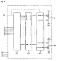
- FIG. 4 is a block diagram illustrating construction of a common data IC.
- FIG. 3 shows a driving waveform for explaining a method of driving a plasma display panel according to the present invention.
- driving margin is secured by applying a control pulse in a sustain period with RGB phosphors having different pulse widths, and driving margin is secured through a combination of X electrodes to which control pulses are applied and X electrodes which are grounded.
- control pulses having a different width are biased to the X electrodes with a voltage Va during sustain period every RGB phosphors, thereby controlling wall charges of the X electrodes. Further, in order to control wall charges, the amount of the wall charges formed in the X electrodes is controlled by applying control pulses having voltage Va to the X electrodes or not applying it, i.e., grounding X electrodes.
- a stabilized reset operation is performed in the G phosphor region since a reset voltage is high.
- the control pulse is applied only to a X electrode corresponding to the R phosphor in the sustain period before the reset voltage is applied.
- the amount of wall charges formed in the X electrodes corresponding to the R phosphor is smaller than those formed in X electrodes corresponding to the B phosphor and the G phosphor. It is thus possible to prevent erroneous discharge from occurring in the R phosphor region in the reset period.
- the driving method according to the present invention can be applied to various situations, which are generated due to not only the reset operation but also different characteristics of the R, G and B phosphors.
- the method of driving the plasma display panel which is implemented using a waveform as shown in FIG. 3, according to the present invention can be implemented through control of only a data IC included in the X electrode driving unit 130 without an additional circuit.
- the data IC receives data from the data alignment unit 120, and applies a data pulse corresponding to one sub-field to X electrodes.
- FIG. 4 is a block diagram illustrating construction of a common one data IC.
- the method of driving the plasma display panel according to the present invention can be implemented without an additional circuit by using a common data IC.
- the common data IC includes a shift register 471, a latch 473 and an output logic unit 475.
- data received through 4 input pins are stored in the shift register 471 during 16 clocks, and are then output to the latch 473.
- the latch 473 allows the data to be applied to the X electrodes through 96 output pins in a scan process.
- This general data IC is controlled by control signals BLK, POC and STB received from the data alignment unit 120.
- the following table shows a true table for the operation of the common data IC.
- Qn indicates data received from the data alignment unit
- L indicates a LOW level
- H indicates a HIGH level
- X indicates that both L and H are possible.
- the plasma display panel performs an addressing operation for 480 lines.
- the data IC when the data IC performs 481 th addressing, the data IC receives the STB signal of a HIGH level, the BLK signal of a HIGH level and the POC control signal of a HIGH level from the data alignment unit 120, and applies a control pulse to a X electrode corresponding to one of the R, G and B phosphors. Thereafter, if the data IC receives the STB signal of a LOW signal, the BLK signal of a HIGH level and the POC control signal of a HIGH level, the value by the control pulse keeps intact until the STB control signal becomes a HIGH level.
- the control pulse serves to bias Va to the X electrode corresponding to the R phosphor in the sustain period.
- the shift register 471 sends 96 data to the latch 473 during the 16 clocks.
- the latch 473 temporarily stores the data, and then transmits the data to the output logic unit 475.
- the output logic unit 475 drives the X electrodes according to the data.
- the data electrode driving unit applies an additional control pulse corresponding to the data electrode driving voltage Va to the X electrode corresponding to one of R, G and B phosphors in the sustain period.
- the data electrode driving unit controls the width of the control pulse according to characteristics of the phosphors.
- the width of the control pulse can be controlled by applying the BLK signal as the voltage Va and then selecting a time point where the BLK signal is changed to the ground state, as described above. That is, if the time point where the BLK signal is changed to the ground state after the voltage Va is applied is long, the pulse width becomes lengthy, and vice verse.
- a common data IC is controlled to apply a control pulse to a X electrode corresponding to each of phosphors in a sustain period.
- a control pulse is applied to each of X electrodes corresponding to R, G and B phosphors. Therefore, the present invention is advantageous in that it can secure driving margin without an additional circuit.
Landscapes
- Engineering & Computer Science (AREA)
- Physics & Mathematics (AREA)
- Power Engineering (AREA)
- Plasma & Fusion (AREA)
- Computer Hardware Design (AREA)
- General Physics & Mathematics (AREA)
- Theoretical Computer Science (AREA)
- Life Sciences & Earth Sciences (AREA)
- Health & Medical Sciences (AREA)
- Animal Behavior & Ethology (AREA)
- General Health & Medical Sciences (AREA)
- Public Health (AREA)
- Veterinary Medicine (AREA)
- Food Science & Technology (AREA)
- Mechanical Engineering (AREA)
- Control Of Indicators Other Than Cathode Ray Tubes (AREA)
Abstract
Description
| On | STB | BLK | POC | Output | Note |
| X | X | L | X | All L | Output LOW level |
| X | X | H | L | All H | Output HIGH level |
| X | H | H | H | On | Latch data |
| L | L | H | H | L | Sustain data |
| H | L | H | H | H | Sustain data |
Claims (8)
- A plasma display apparatus including a data electrode driving unit for applying data for light-emitting R, G and B phosphors to data electrodes, a scan electrode driving unit for applying a scan pulse and a sustain pulse to a scan electrode, and a sustain electrode driving unit for applying a sustain pulse to a sustain electrode,
wherein the data electrode driving unit applies a control pulse to the data electrode corresponding to one of the R, G and B phosphors in a sustain period where the sustain pulse is applied to the scan electrode and the sustain electrode. - The plasma display apparatus as claimed in claim 1, wherein the data electrode driving unit controls the widths of the control pulses differently according to characteristics of the R, G and B phosphors.
- The plasma display apparatus as claimed in claim 1, wherein the data electrode driving unit controls the amount of wall charges by applying the control pulse to the data electrode or grounding the data electrode
- The plasma display apparatus as claimed in claim 2, wherein the data electrode driving unit controls the width of the control pulse by selecting a time point where application of the control pulse is finished.
- A method of driving a plasma display apparatus including a data electrode driving unit for applying data for light-emitting R, G and B phosphors to data electrodes, a scan electrode driving unit for applying a scan pulse and a sustain pulse to a scan electrode, and a sustain electrode driving unit for applying a sustain pulse to a sustain electrode,
wherein the data electrode driving unit applies a control pulse to data electrode corresponding to one of the R, G and B phosphors in a sustain period where the sustain pulse is applied to the scan electrode and the sustain electrode. - The method as claimed in claim 5, wherein the data electrode driving unit controls the widths of the control pulses differently according to characteristics of the R, G and B phosphors.
- The method as claimed in claim 5, wherein the data electrode driving unit controls the amount of wall charges by applying the control pulse to the data electrode or grounding the data electrode.
- The method as claimed in claim 6, wherein the data electrode driving unit controls the width of the control pulse by selecting a time point where application of the control pulse is finished.
Applications Claiming Priority (2)
| Application Number | Priority Date | Filing Date | Title |
|---|---|---|---|
| KR1020040010504A KR20050082124A (en) | 2004-02-17 | 2004-02-17 | Method for driving plasma display panel |
| KR2004010504 | 2004-02-17 |
Publications (2)
| Publication Number | Publication Date |
|---|---|
| EP1566792A2 true EP1566792A2 (en) | 2005-08-24 |
| EP1566792A3 EP1566792A3 (en) | 2007-05-16 |
Family
ID=34709342
Family Applications (1)
| Application Number | Title | Priority Date | Filing Date |
|---|---|---|---|
| EP05002906A Ceased EP1566792A3 (en) | 2004-02-17 | 2005-02-11 | Apparatus for driving plasma display panel |
Country Status (3)
| Country | Link |
|---|---|
| US (1) | US20050179620A1 (en) |
| EP (1) | EP1566792A3 (en) |
| KR (1) | KR20050082124A (en) |
Families Citing this family (1)
| Publication number | Priority date | Publication date | Assignee | Title |
|---|---|---|---|---|
| KR100670362B1 (en) * | 2005-11-29 | 2007-01-16 | 삼성에스디아이 주식회사 | Display device |
Citations (6)
| Publication number | Priority date | Publication date | Assignee | Title |
|---|---|---|---|---|
| JPH10333639A (en) | 1997-05-29 | 1998-12-18 | Matsushita Electric Ind Co Ltd | Image display device |
| EP0905738A2 (en) | 1997-09-29 | 1999-03-31 | Hitachi, Ltd. | Display device and driving method thereof |
| JPH11119728A (en) | 1997-10-09 | 1999-04-30 | Fujitsu Ltd | Driving method of AC PDP and plasma display device |
| US6400347B1 (en) | 1998-01-23 | 2002-06-04 | Lg Electronics Inc. | Method for driving sustain lines in a plasma display panel |
| EP1244088A2 (en) | 2001-03-19 | 2002-09-25 | Fujitsu Limited | Method of driving a plasma display panel |
| WO2002099779A1 (en) | 2001-06-02 | 2002-12-12 | Yeint Co., Ltd. | Control method and system for improving luminance, luminous efficiency and color temperature in an ac-pdp |
Family Cites Families (2)
| Publication number | Priority date | Publication date | Assignee | Title |
|---|---|---|---|---|
| FR2772502B1 (en) * | 1997-12-15 | 2000-01-21 | Thomson Multimedia Sa | METHOD FOR COMPENSATING FOR DIFFERENCES IN THE REMANENCE OF LUMINOPHORES IN AN IMAGE VIEWING SCREEN |
| TW200421233A (en) * | 2002-11-29 | 2004-10-16 | Matsushita Electric Industrial Co Ltd | Plasma display panel device and related drive method |
-
2004
- 2004-02-17 KR KR1020040010504A patent/KR20050082124A/en not_active Ceased
-
2005
- 2005-02-11 EP EP05002906A patent/EP1566792A3/en not_active Ceased
- 2005-02-11 US US11/055,084 patent/US20050179620A1/en not_active Abandoned
Patent Citations (6)
| Publication number | Priority date | Publication date | Assignee | Title |
|---|---|---|---|---|
| JPH10333639A (en) | 1997-05-29 | 1998-12-18 | Matsushita Electric Ind Co Ltd | Image display device |
| EP0905738A2 (en) | 1997-09-29 | 1999-03-31 | Hitachi, Ltd. | Display device and driving method thereof |
| JPH11119728A (en) | 1997-10-09 | 1999-04-30 | Fujitsu Ltd | Driving method of AC PDP and plasma display device |
| US6400347B1 (en) | 1998-01-23 | 2002-06-04 | Lg Electronics Inc. | Method for driving sustain lines in a plasma display panel |
| EP1244088A2 (en) | 2001-03-19 | 2002-09-25 | Fujitsu Limited | Method of driving a plasma display panel |
| WO2002099779A1 (en) | 2001-06-02 | 2002-12-12 | Yeint Co., Ltd. | Control method and system for improving luminance, luminous efficiency and color temperature in an ac-pdp |
Also Published As
| Publication number | Publication date |
|---|---|
| EP1566792A3 (en) | 2007-05-16 |
| KR20050082124A (en) | 2005-08-22 |
| US20050179620A1 (en) | 2005-08-18 |
Similar Documents
| Publication | Publication Date | Title |
|---|---|---|
| US8179342B2 (en) | Method and apparatus for driving plasma display panel | |
| US20050225513A1 (en) | Plasma display device and method of driving the same | |
| EP1553550B1 (en) | Method and apparatus of driving a plasma display panel | |
| US7663573B2 (en) | Plasma display panel and driving method thereof | |
| KR20040034275A (en) | Plasma display panel and method for driving the same | |
| EP1596412A2 (en) | Plasma display apparatus and method of driving the same | |
| US7868849B2 (en) | Plasma display apparatus and method of driving the same | |
| JP2005196194A (en) | Method and apparatus for driving plasma display panel | |
| US7852294B2 (en) | Plasma display apparatus and driving method thereof | |
| EP1659559B1 (en) | Plasma display apparatus and driving method thereof | |
| EP1566792A2 (en) | Apparatus for driving plasma display panel | |
| US7642992B2 (en) | Plasma display apparatus and driving method thereof | |
| US7486259B2 (en) | Plasma display panel and method for driving the same | |
| JP2002358047A (en) | Driving method of plasma display panel using selective inversion address system | |
| US20060001609A1 (en) | Plasma display apparatus and driving method thereof | |
| US20090189885A1 (en) | Plasma display panel and method and device for driving the same | |
| KR19980075059A (en) | Plasma display device | |
| KR100599655B1 (en) | Plasma display device and driving method thereof | |
| KR20060093322A (en) | Driving Method of Plasma Display Panel | |
| US20070085773A1 (en) | Plasma display apparatus | |
| US7619586B2 (en) | Plasma display apparatus and method for driving the same | |
| KR100502930B1 (en) | Apparatus and method for driving plasma display panel | |
| US20060238453A1 (en) | Plasma display apparatus and driving method thereof | |
| US20090040145A1 (en) | Plasma display device and driving method thereof | |
| JP2000227781A (en) | Plasma display panel driving device and plasma display device |
Legal Events
| Date | Code | Title | Description |
|---|---|---|---|
| PUAI | Public reference made under article 153(3) epc to a published international application that has entered the european phase |
Free format text: ORIGINAL CODE: 0009012 |
|
| AK | Designated contracting states |
Kind code of ref document: A2 Designated state(s): AT BE BG CH CY CZ DE DK EE ES FI FR GB GR HU IE IS IT LI LT LU MC NL PL PT RO SE SI SK TR |
|
| AX | Request for extension of the european patent |
Extension state: AL BA HR LV MK YU |
|
| PUAL | Search report despatched |
Free format text: ORIGINAL CODE: 0009013 |
|
| AK | Designated contracting states |
Kind code of ref document: A3 Designated state(s): AT BE BG CH CY CZ DE DK EE ES FI FR GB GR HU IE IS IT LI LT LU MC NL PL PT RO SE SI SK TR |
|
| AX | Request for extension of the european patent |
Extension state: AL BA HR LV MK YU |
|
| RIC1 | Information provided on ipc code assigned before grant |
Ipc: G09G 3/288 20060101AFI20070411BHEP |
|
| 17P | Request for examination filed |
Effective date: 20071115 |
|
| AKX | Designation fees paid |
Designated state(s): DE FR GB NL |
|
| 17Q | First examination report despatched |
Effective date: 20080206 |
|
| STAA | Information on the status of an ep patent application or granted ep patent |
Free format text: STATUS: THE APPLICATION HAS BEEN REFUSED |
|
| 18R | Application refused |
Effective date: 20090127 |