Background of the Invention
1. Field of the Invention
The present invention relates to image memories
and image processing apparatuses using the same. More
specifically, the present invention relates to
improvement in methods for writing image data onto
image memories.
2. Description of the Related Art
Display devices, such as liquid crystal
displays, often incorporate an image memory for
storing image data. Such display devices are designed
to store image data generated by an image processor,
such as a CPU and a digital signal processor, and to
display images using the image data stored in the
image memory.
Improving the access speed to the image memory
is one of the important requirements for enhancing the
image processing speed within the display device.
Japanese Laid-open Patent Application No. H07-295535,
for instance, discloses a data processing system that
improves the access speed to the image memory by
concurrently updating the pixel data for each pixel.
Summary of the Invention
The inventors have discovered that there is
still room for improvement in the access speed to the
image memory with regard to the conventional data
processing system.
In an aspect of the present invention, an image
memory is composed of a memory cell array, first and
second area selecting circuits, and a write circuit.
The memory cell array includes memory elements arrayed
in rows and columns, each of the memory elements being
adapted to store pixel data. The first area selecting
circuit is adapted to select a plurality of row
addresses at the same time, and the second area
selecting circuit is adapted to select a plurality of
column addresses at the same time. The write circuit
is adapted to write same pixel data into selected
memory elements out of the memory elements, the
selected memory elements being associated with the
selected row addresses and column addresses.
Such image memory architecture is adapted to
write pixel data for multiple pixels onto the image
memory at the same time, and thereby effectively
enhances the access speed to the image memory.
In another aspect of the present invention, an
image processing apparatus is composed of a drawing
circuit and an image memory. The drawing circuit is
designed to define a rectangular area within an image
so that the rectangular area incorporates pixels
associated with same pixel data. The image memory is
adapted to store the image. The image memory includes
a memory cell array, first and second area selecting
circuit, and a write circuit. The memory cell array
includes memory elements arrayed in rows and columns.
The first area selecting circuit is adapted to select
a plurality of row addresses associated with the
rectangular area at the same time, and the second area
selecting circuit is adapted to select a plurality of
column addresses associated with the rectangular area
at the same time. The write circuit is adapted to
write same pixel data into selected memory elements
out of the memory elements, the selected memory
elements being associated with the selected row
addresses and column addresses.
In still another aspect of the present
invention, a controller driver is composed of a
control circuit, a drawing circuit, an image memory, a
filter circuit, and a drive circuit. The control
circuit externally receives image bitmap data
associated with an image, and font data associated
with a character. The drawing circuit is designed to
define a rectangular area within the character so that
the rectangular area incorporates pixels associated
with same pixel data. The image memory is used for
storing character image data associated with the
character. The filter circuit is adapted to
synthesize the image bitmap data and the character
image data to develop synthesized image bitmap data.
The drive circuit driving a display panel in response
to the synthesized image bitmap data. The image
memory includes a memory cell array, first and second
area selecting circuits, and a write circuit. The
memory cell array is composed of memory elements
arrayed in rows and columns. The first area selecting
circuit is adapted to select a plurality of row
addresses associated with the rectangular area at the
same time, and the second area selecting circuit
adapted to select a plurality of column addresses
associated with the rectangular area at the same time.
The write circuit is adapted to write the same pixel
data into selected memory elements out of the memory
elements to develop the character image data
incorporating the same pixel data onto the memory cell
array, the selected memory elements being associated
with the selected row addresses and column addresses.
In still another aspect of the present
invention, a method for writing image data onto an
image memory including memory elements arrayed in rows
and columns is composed of:
Brief Description of the Drawings
A better understanding of the present invention
is made by reading a detailed description in
conjunction with the accompanying drawings, in which:
Description of the Preferred Embodiments
It should be understood that the following
indexes are merely provided in order to achieve better
understandings of a detailed description of the
present invention.
First Embodiment
1) Entire Device Structure
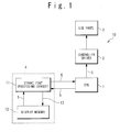
Fig. 1 schematically shows an exemplary
structure of a display device 10 according to a first
embodiment of the present invention. In this
embodiment, the display device 10 is adapted to
achieve high speed processing of stroke font data.
Specifically, the display device 10 is equipped with a
CPU (central processing unit) 1, a controller driver 2,
an LCD (liquid crystal display) panel 3, and a stroke
font processing circuit 4. The LCD panel 3
incorporates pixels arrayed in a matrix. The x-y
coordinate system is defined on the LCD panel 3 by a
set of x and y axes, the x axis being defined along
the horizontal direction of the LCD panel 3, and the y
axis is defined along the vertical direction. The
respective pixels of the LCD panel 3 may be addressed
by an x address (namely, column address) and a y
address (namely, row address).
The CPU 1 generates font data 6 associated with
characters contained in a display image to be
displayed on the LCD panel 3. The font data 6 is
generated in a stroke font format, which represents
each character with a shape and sort of a line.
Specifically, the font data 6 is composed of commands,
each representing a line incorporated in the
associated character. Each command includes
coordinates of control points, sort data indicative of
a sort of the line, pixel data of pixels incorporated
within the line, width data representative of a width
of the line. The control points are used to define
the position and the shape of the line. The pixel
data typically include color data representative the
colors of the relevant pixels in an RGB format. In a
typical architecture, the font data 6 is generated
using a font memory, which stores therein font data
for all the usable characters.
The stroke font processing circuit 4 is
designed to generate the image data of the display
image composed of the characters. In this embodiment,
the image data is generated in a bitmap format. It
should be understood that image data produced by the
stroke font processing circuit 4 will be referred to
as "bitmap data 5" hereinafter. The bitmap data 5 is
composed of pixel data for designating the color of
each pixel within the LCD panel 3. The produced
bitmap data 5 is transmitted via the CPU 1 to the
controller driver 2.
In response to the bitmap data 5, the
controller driver 2 drives the LCD panel 3 to display
desired characters on the LCD panel 3.
The stroke font processing circuit 4 is
equipped with a stroke font drawing circuit 11 and an
image memory 12. The stroke font drawing circuit 11
sequentially interprets commands contained in the font
data 6 to produce the bitmap data 5 of the
corresponding characters in response to the font data
6 onto the image memory 12. Such an operation that
the stroke font drawing circuit 11 produces bitmap
data 5 associated with characters onto the image
memory 12 may be also represented using the term "to
draw characters", hereinafter. The image memory 12 is
used as a work area for generating the bitmap data 5.
After the stroke font drawing circuit 11 completes "to
draw characters" onto the image memory 12, and the
associated bitmap data 5 is developed onto the image
memory 12. The bitmap data 5 generated by the stroke
font drawing circuit 11 is then transmitted via the
CPU 1 to the controller driver 2.
Improving in write speeds of pixel data onto
the image memory 12 is one of the important aspects
for enhancing the operation speed of the stroke font
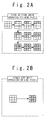
processing circuit 4. As shown in Fig. 2A, a
conventional image memory architecture write pixel
data onto an image memory "pixel-by-pixel". For
instance, a writing operation as to pixel data
associated with pixels arranged in three rows and
three columns is subdivided into 9 times of write
operations. In this conventional writing method,
multiple writing cycles are required in order to write
the pixel data; the total number of necessary writing
cycles being equal to the number of the pixels
associated to the pixel data. This conventional
method is not suitable for high-speed generation of
the bitmap data 5.
On the other hand, the display device 10 of
this embodiment achieves high-speed data write of the
pixel data onto the image memory 12 through making use
of a fact that each character is drawn with a single
color; all the pixels relevant to the character are
programmed with the same pixel data associated with
the color of the character. Specifically, as shown in
Fig. 2B, the image memory 12 of the first embodiment
is designed to simultaneously write the pixel data
onto the image memory 12 for a set of pixels relevant
to a certain rectangular area involved in a character,
when the pixels are to be programmed with the same
pixel data. Such a data writing process is
advantageous for writing the image data of the image
constructed of characters, because pixels relevant to
a character are normally programmed with the same
pixel data. Exemplary structures and operations of
the font drawing circuit 11 and the image memory 12
will be described in detail in the following.
2) Structure and Operation of Stroke Font Drawing
Circuit
As previously described, the stroke font
drawing circuit 11 provides "drawing of characters"
onto the image memory 12 in response to the font data
6.
Schematically, the stroke font drawing circuit
11 operates as follows: The stroke font drawing
circuit 11 recognizes a shape of a character to be
displayed from the font data 6, and defines a set of
rectangular areas in the recognized character so that
the pixels within each rectangular area are programmed
with the same pixel data. As will be described later,
two or more of the rectangular areas used to represent
a character may be overlapped with one another.
Additionally, as shown in Fig. 1, the font
drawing circuit 11 produces rectangular area data 13
each associated with the rectangular areas. The
rectangular area data 13 includes coordinates of a
reference point of the associated rectangular area, a
width "W" of the associated rectangular area along the
x axis direction, a height "h" of the associated
rectangular area along the y axis direction, and the
pixel data of the pixels contained in the associated
rectangular area. The width "W" of each rectangular
area is represented by the number of the pixels
arranged in one row, and therefore the width "W" is a
natural number. Correspondingly, the height "h" of
each rectangular area is represented by the number of
the pixels arranged in one column. A set of
coordinates of the reference point may be referred to
as "reference coordinates", hereinafter, and x and y
coordinates of the reference point may be denoted by
symbols "x0" and "y0", respectively.
The reference coordinates (x0, y0) within the
rectangular area data 13 are used to designate a
position of each rectangular area. It should be noted
that the reference coordinates may be defined as being
coordinates of any position within the rectangular
area. For instance, the reference coordinates may be
defined as being coordinates of the center point of
each rectangular area, and/or may be defined as
coordinates of the corner(s) of the relevant
rectangular area. It should be also noted that the
position of each rectangular area is preferably
designated by the coordinates of the center point
thereof, because this facilitates the calculation of
the position of the each rectangular area; the font
data 6, represented in the stroke font format,
expresses each character with the shapes of the center
lines of the relevant character and the sort of the
lines (including color of each line). In this
embodiment, the reference coordinates (x0, y0) may be
defined as the coordinates of the center point of each
rectangular area.
The rectangular area data 13 produced by the
stroke font drawing circuit 11 is transmitted to the
image memory 12. The pixel data of the pixels within
the rectangular areas, described in the rectangular
area data 13, is written onto the image memory 12 to
complete "drawing of the characters". The pixel data
of the pixels contained in a certain rectangular area
is written onto the image memory 12 at the same time,
for achieving high-speed write of the pixel data for
the relevant pixels.
3) Structure and Operation of Image Memory
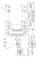
Fig 5 is a block diagram for schematically
showing an exemplary structure of the image memory 12.
The image memory 12 is composed of a Y address control
circuit 21, a Y area selecting circuit 22, a word line
decoder 23, an X address control circuit 24, an X area
selecting circuit 25, a bit line decoder 26, and a
memory cell array 27. The memory cell array 27 is
equipped with pixel blocks 33, word lines 31, and bit
line 32. The pixel blocks 33 each functions as a
pixel data storage element storing the associated
pixel data; the pixel blocks 33 are associated with
the respective pixels within the LCD panel 3 in the
one-to-one correspondence. Each pixel block 33 stores
the pixel data of the associated pixel. The pixel
blocks 33 are addressable using a set of x and y
addresses of the associated pixel. The pixel blocks
33 are each composed of n memory cells 34 arrayed
along the horizontal direction (x direction) to store
therein n-bit pixel data. In this embodiment, the
pixel blocks 33 are each designed to store 24-bit
pixel data composed of 8-bit R (red) data, 8-bit G
(green) data, and 8-bit B (blue) data. The memory
cells 34 are located at the respective intersections
of the word lines 31 and the bit lines 32. A set of
the memory cells 34 storing the pixel data of a
desired pixel is accessible through addressing the
desired word line 31 and bit line 32 by using the x
and y addresses of the desired pixel.
The Y address control circuit 21 calculates a
set of the maximum value "yMAX" and minimum value "yMIN"
of y addresses of the relevant rectangular area
indicated in the rectangular area data 13 on the basis
of the y reference coordinate "y0" and the height "h"
of the relevant rectangular area. Various calculation
methods may be used for determining the maximum value
yMAX and minimum value of yMIN of the y addresses of the
relevant rectangular area.
In one embodiment, different formulas may be
used for determining the maximum value yMAX and minimum
value yMIN depending on whether the height "h" is an
odd number or an even number. In this embodiment, for
a height "h" being an odd number, the maximum value
yMAX and minimum value yMIN may be calculated using the
following formulas:
yMAX = y0 + h/2,
and
yMIN = y0 - h/2,
while being calculated using the following formulas:
yMAX = y0 + h/2,
and
yMIN = y0 - h/2 - 1,
for a height "h" being an even number. Alternatively,
the maximum value yMAX and minimum value yMIN for a
height "h" being an even number may be calculated by
the following formulas:
yMAX = y0 + h/2 - 1,
and
yMIN = y0 - h/2.
In an alternative embodiment, the maximum value
yMAX and minimum value yMIN of the y address may be
calculated by the following formulas:
yMAX = y0 + h,
and
yMIN = y0,
independently of whether the height "h" is an odd
number of an even number. Instead, the maximum value
yMAX and minimum value yMIN may be calculated by the
following formulas:
yMAX = y0,
and
yMIN = y0 - h.
The Y area selecting circuit 22 outputs y
address signals "280" to "28M-1" to the word line
decoder 23 in response to the maximum value yMAX and
the minimum value yMIN of the relevant rectangular area.
It should be also noted that the symbol "M" denotes a
number of rows in which the pixel blocks 33 are
arrayed. This implies that the y address of the pixel
ranges from 0 to M-1. The Y area selecting circuit 22
activates selected one(s) of the y address signals 280
to 28M-1 which are associated with the y addresses of
yMIN to yMAX. It should be understood that two or more
of the y addresses may be selected for a single write
operation.
The word line decoder 23 activates selected
one(s) of the word lines 31 in response to the y
address signals 280 to 28M-1. When a plurality of y
addresses are selected, a plurality of word lines
associated with selected y addresses are activated at
the same time. This provides electrical connections
between the associated memory cells 34 and bit lines
32.
Similarly to the Y address control circuit 21,
the X address control circuit 24 is designed to
calculate the maximum value "xMAX" and minimum vale
"xMIN" of the x addresses of the rectangular area
indicated in the rectangular area data 13 on the basis
of the x reference coordinate "x0" and the width "W"
of the relevant rectangular area. Various calculation
methods may be used for determining the maximum value
xMAX and minimum value xMIN.
In one embodiment, different formulas may be
used for determining the maximum value xMAX and minimum
value xMIN depending on whether the width "W" is an odd
number or an even number. In this embodiment, for a
width "W" being an odd number, the maximum value xMAX
and minimum value xMIN may be calculated using the
following formulas:
xMAX = x0 + W/2,
and
xMIN = x0 - W/2,
while being calculated using the following formulas:
xMAX = x0 + W/2,
and
xMIN = x0 - W/2 - 1,
for a height "h" being an even number. Alternatively,
the maximum value xMAX and minimum value xMIN for a
height "h" being an even number may be calculated by
the following formulas:
xMAX = x0 + W/2 - 1,
and
xMIN = x0 - W/2.
In an alternative embodiment, the maximum value
xMAX and minimum value xMIN of the x address may be
calculated by the following formulas:
xMAX = x0 + W,
and
xMIN = X0,
independently of whether the width "W" is an odd
number of an even number. Instead, the maximum value
xMAX and minimum value xMIN may be calculated by the
following formulas:
xMAX = x0,
and
xMIN = x0 - W.
The X area selecting circuit 25 provides x
address signals 290 to 29N-1 to the bit line decoder 26
in response to the maximum value xMAX and minimum value
xMIN of the x addresses of the relevant rectangular
area. The x address signals 290 to 29N-1 are
representative of whether or not the respective x
addresses are selected. It should be noted that the
symbol "N" denotes the number of columns in which the
pixel blocks 42 are arrayed. This implies that the x
addresses ranges from 0 to N-1. The X area selecting
circuit 25 activates selected one(s) of the x address
signals 290 to 29N-1 which are associated with a set of
selected x addresses, that is, the x addresses from
xMIN to xMAX. It should also be understood that a
plurality of x addresses may be selected during a
single write operation. Desired one(s) of the pixel
blocks 33 are selected using the y address(es)
selected by the Y area selecting circuit 22 and the x
address(es) selected by the X area selecting circuit
25.
The bit line decoder 26 is responsive to the x
address signals 290 to 29N-1 for connecting selected
ones of bit lines 32 associated with the selected x
address(es) to the n signal lines used to transfer the
pixel data within the rectangular area data 13 to the
image memory 12. This completes writing the pixel
data into the selected one(s) of the pixel blocks 33,
that is, writing the data bits of the pixel data into
the associated memory cells 34 of the selected the
pixel block(s) 33.
The aforementioned architecture allows the
image memory 12 to select the pixel blocks 33
positioned over multiple rows and/or columns
positioned within the relevant rectangular area, and
to write the pixel data onto the selected pixel blocks
33 at the same time.
4) Structure and Operation of Y Area selecting Circuit
and X Area Selecting Circuit
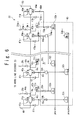
Fig. 6 is a circuit diagram illustrating an
exemplary structure of the Y area selecting circuit 22.
The Y area selecting circuit 22 is provided with
transfer gates 410 to 41M-1, N-channel MOS transistors
420 to 42M-1, a logic circuit 43, and output inverters
440 to 44M-1. The transfer gates 410 to 41M-1 and the N-channel
MOS transistors 420 to 42M-1 function as switch
elements.
The transfer gates 410 to 41M-1 are series-connected
between power supply terminals 49 and 50.
The transfer gate 410, positioned at one end of the
series-connected transfer gates, is interposed between
the power supply terminal 49 and an output node N0.
The transfer gate 41M-1, positioned at another end of
the series-connected transfer gates, is interposed
between an output mode NM-1 and the power supply
terminal 50. The transfer gate 41i is interposed
between an output node Ni-1 and an output node Ni. In
other words, the output node Ni electrically couples
the transfer gate 41i to the transfer gate 41i+1.
Each transfer gate 41i is equipped with an N-channel
MOS transistor 45i, a P-channel MOS transistor
46i, and an inverter 47i. The N-channel MOS transistor
45i and the P-channel MOS transistor 46i have commonly-coupled
sources and drains. The input of the inverter
47i and the gate of the MOS transistor 46 are
connected to a control terminal 48i, and the output of
the inverter 47i is connected to the gate of the N-channel
MOS transistor 46i.
The transfer gates 410 to 41M-1 are turned on or
off in response to potentials of the control terminals
480 to 48M-1, respectively. When the control terminals
480 to 48M-1 are pulled down to the ground potential,
the transfer gates 410 to 41M-1 are turned off. When
the control terminals 480 to 48M-1 are pulled up to the
power supply potential, on the other hand, the
transfer gates 410 to 41M-1 are turned on.
The N-channel MOS transistors 420 to 42M-1 are
interposed between the output nodes N0 to NM-1 and the
ground terminals 510 to 51M-1, respectively. A drain of
the N-channel MOS transistor 42i is connected to the
output node Ni, and a source thereof is connected to
the ground terminal 51i.
The logic circuit 43 controls the transfer
gates 410 to 41M-1 and the N-channel MOS transistors 420
to 42M-1 in response to the maximum value yMAX and the
minimum value yMIN of the y addresses of the relevant
rectangular area.
A detailed structure of the logic circuit 43 is
given in the following. The logic circuit 43 is
equipped with decoder circuits 520 to 52M-1, decoder
circuits 530 to "53M-1, an inverter 540, NAND gates 542
to 54M-1, and inverters 550 to 55M-1. The decoder
circuits 520 to 52M-1 are designed to pulls up or down
the outputs thereof in response to the maximum value
yMAX of the y address of the rectangular; the decoder
circuit 52i pulls down the output to the "Low" level
when the maximum value yMAX is "i"; otherwise the
decoder circuit 52i pulls up the output to the "High"
level. Correspondingly, the decoder circuit 53i pulls
down the output to the "Low" level when the maximum
value yMIN is "i", and pulls up the output to the
"High" level, when the maximum value yMIN is not "i".
The outputs of the decoder circuits 520 to 52M-1 are
connected via the inverters 550 to 55M-1 to the gates
of the N-channel MOS transistors 420 to 42M-1,
respectively. An output of the decoder circuit 52M-1
located at the end is further connected via the
inverter 55M-1 to the control terminal 48M of the
transfer gate 41M.
On the other hand, the output of the decoder
circuit 530, which receives the minimum value yMIN, is
connected to an input of the inverter 540, and an
output of the inverter 540 is connected to the control
terminal 480. The outputs of the remaining decoder
circuits 542 to 53M-1 are connected to first inputs of
NAND gates 542 to 54M-1, respectively. Second inputs of
the NAND gates 542 to 54M-1 are connected to the
outputs of the decoder circuits 520 to 52M-1,
respectively. The outputs of the NAND gates 542 to
54M-1 are connected to the control terminals 482 to 48M-1,
respectively.
Inputs of the output inverters 440 to 44M-1 are
connected to output nodes "N0" to "NM-1", respectively.
The y address signals 280 to 28M-1 are outputted from
the outputs of the output inverters 440 to 44M-1.
Fig. 7 is a conceptual diagram illustrating an
exemplary operation of the Y area selecting circuit
22; the illustration in Fig. 7 assumes that the
maximum value yMAX is "3" and the minimum value yMIN is
"1". When the logic circuit 43 receives the maximum
value yMAX and minimum value yMIN of the y addresses of
the relevant rectangular area, the logic circuit 43
turns off the transfer gate "41yMAX + 1", and a transfer
gate "41yMIN", while turning on the remaining transfer
gates 41. Further, the logic circuit 43 turns on the
N-channel MOS transistor 42yMAX and turns off the
remaining N-channel MOS transistors 42. This results
in that the output nodes NyMIN to NyMAX are pulled down
to the "Low" level, and the remaining output nodes are
pulled up to the "High" level. This results in that
the y address signals 28yMIN to 28yMAX are pulled up to
the "High" level while the remaining y address signals
28 are pulled down to the "Low" level, in other words,
the y addresses yMIN to yMAX, associated with the
relevant rectangular area, are selected.
Enhancing the operation speed of the Y area
selecting circuit 22 requires high-speed pull-up of
the output nodes associated with the Y address signals
28 to be deactivated; however, the structure of the Y
area selecting circuit 22 shown in Fig. 6 may be
unsuitable for high-speed pull-up of the relevant
output nodes. Specifically, the structure of the Y
area selecting circuit 22 shown in Fig. 6 requires
connecting the desired output nodes via one ore more
transfer gates 41 to either the power supply terminal
49 or the power supply terminal 50 for pulling up the
desired output nodes. Therefore, the pull-up of the
desired output nodes may undesirably require a long
duration due to the on-resistance of the transfer
gates 41, in particular, for a case that the output
nodes to be pulled up are connected via a large number
of the transfer gates 41 to the power supply terminal
49 (or power supply terminal 50).
In order to reduce the duration required to
pull up the desired output nodes, it is preferable
that the output nodes N0 to NM-1 are precharged to
"High" level before the y address signals 280 to 28M-1
are driven to desired levels. Fig. 8 illustrates a
preferred structure of the Y area selecting circuit 22,
which is adapted to precharge the output nodes N0 to
NM-1 to the "High" level. In this structure, a set of
P-channel MOS transistors 560 to 56M-1 are additionally
provided for the Y area selecting circuit 22. Sources
of the P-channel MOS transistors 560 to 56M-1 are
connected to power supply terminals 570 to 57M-1, and
drains thereof are connected to the output nodes N0 to
NM-1. A precharge control signal 59 is inputted to
gates of the P-channel MOS transistors 560 to 56M-1.
The output nodes N0 to NM-1 are electrically connected
to the powers supply terminals 570 to 57M-1,
respectively in response to the pull-down of the
precharge control signal 57.
Another approach for enhancing the operation
speed of the Y area selecting circuit 22 is to provide
high-speed pull-down for the output nodes associated
with the Y address signals 280 to 29M-1 to be activated.
This approach is preferably achieved through pulling
down the desired output nodes to the "Low" level using
two or more of the N-channel MOS transistors 42.
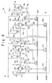
Fig. 9 is a circuit diagram illustrating an
exemplary structure of the Y area selecting circuit 22,
which is adapted to pull down the desired output nodes
using two or more of the MOS transistors 42. The
structure of the Y area selecting circuit 22 shown in
Fig. 9 is different from that shown in Fig. 8 in the
structure of the logic circuit 43; the logic circuit
43 of Fig. 9 additionally includes NAND gates 580 to
58M-1. One input of the NAND gate 58i is connected to
the output of a first decoder 52i and the output of
the second decoder 53i, and another input of the NAND
gate 58i is connected to the output of the inverter 55i.
The output of the NAND gate 58i is connected to the
gate of the N-channel MOS transistor 42i.
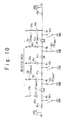
Fig. 10 is a conceptual diagram representing
operations of the Y area selecting circuit 22 of Fig.
9; the illustration in Fig. 10 assumes that the
maximum value yMAX is "3" and the minimum value yMIN is
"1". When the logic circuit 43 receives the maximum
value yMAX and minimum value yMIN of the y addresses of
the rectangular area, the logic circuit 43 turns off
the transfer gate 41yMAX+1 and the transfer gate 41yMIN,
while turning on the remaining transfer gates 41.
Additionally, the logic circuit 43 turns on the two N-channel
MOS transistors 42yMAX, 42yMIN, while turning off
the remaining N-channel MOS transistors 42. As a
result, the output nodes NyMIN to NyMAX are pulled down
to the "Low" level, and the remaining output nodes are
pulled up to the "High" level. This results in that
the y address signals 28yMIN to 28yMAX are selectively
pulled up to the "High" level, in other words, the y
addresses yMIN to yMAX, associated with the relevant
rectangular area are selected.
As will be understood from Fig. 10, the Y area
selecting circuit 22 of Fig. 9 effectively reduces the
duration required to pull down the desired output
nodes NyMIN to NyMAX, through using the two N-channel MOS
transistors 42yMAX and 42yMIN for the pull-down of the
desired output nodes NyMIN to NyMAX.
It should also be understood that the ground
terminal may be alternatively connected to the
transfer gates 410 and 41M instead of the power supply
terminals 49 and 50; the power supply terminal may be
alternatively connected to the N-channel MOS
transistors 420 to 42M-1 instead of the ground
terminals 510 to 51M-1; and the ground terminal may be
alternatively to the P-channel transistors 560 to 56M-1
instead of the power supply terminals 570 to 57M-1. In
this alternative case, it is suitable that transfer
gates are used instead of the N-channel MOS
transistors 420 to 42M-1.
The structure and operations of the X-area
selecting circuit 25 are basically similar to those of
the Y area selecting circuit 22. The difference
exists in the number of elements that constitute the
X-area selecting circuit 25, and different signals are
inputted to or outputted from the X-area selecting
circuit 25. The X area selecting circuit 25 receives
the maximum value xMAX and minimum value xMIN of the x
addresses of the relevant rectangular area instead of
the maximum value yMAX and the minimum value yMIN of the
y addresses. Furthermore, the X area selecting
circuit 25 is designed to output X-address signals 290
to 29M-1 instead of the Y address signals 280 to 28M-1.
Moreover, the number of the relevant elements is
changed in correspondence with the change in the
number of address signals to be outputted. A detailed
explanation as to the structure and operations of the
X area selecting circuit 23 is omitted, because the
required modification from the Y area selecting
circuit 22 would be apparent to those skilled in the
art.
5) Operation of Display Device
As previously described, the display device in
the first embodiment is designed to convert the font
data 6, represented in the stroke font format, into
the bitmap data 5 using the stroke font processing
circuit 4, and to drive the LCD panel 3 in response to
the bitmap data 5. A detailed description is made of
an exemplary process of the conversion of the font
data 6 into the bitmap data 5.
Referring back to Fig. 1, the font drawing
circuit 11 of the stroke font processing circuit 4
generates the rectangular area data 13 from the font
data 6 as described in the following. The font
drawing circuit 11 acknowledges shapes of lines which
constitute each character to be displayed, and defines
a set of rectangular areas for the respective lines so
that each rectangular area incorporates pixels to be
programmed with the same pixel data; the lines
constituting the characters are represented by the set
of the rectangular areas. The font drawing circuit 11
then produces the rectangular area data 13 for each of
the rectangular areas so that the rectangular area
data 13 indicates the x and y reference coordinates x0,
and y0, the width "W", the height "h" of the
associated rectangular area, and the pixel data with
which the associated pixels are programmed. In this
embodiment, the x and y reference coordinates x0, and
y0 are defined as the center point of each rectangular
area.
Appropriate definition of the rectangular areas
is effective for achieving the requested data write of
the pixel data onto the image memory 12 in a reduced
number of steps. In particular, it is effective for
reducing the number of steps relevant to the data
write of the pixel data to define the rectangular
areas so that two or more of the rectangular areas are
overlapped with each other.
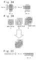
In one embodiment, as shown in Fig. 3A, pixel
data of pixels arranged within a cross-shaped area
having the same color may be written onto the image
memory 12 in accordance with the below-mentioned two
steps: First, pixel data associated with pixels
arranged in five rows and three columns within a first
rectangular area, which pixels are associated with the
same color, is written onto the image memory 12 at the
same time. This is followed by concurrently writing
pixel data associated with pixels arranged in three
rows and five columns within a second rectangular area,
which are associated with the same color. It should
be noted that the second rectangular area is defined
to overlap the first rectangular area. This process
effectively reduces the number of steps necessary for
write the pixel data associated with the pixels
arranged within the cross-shaped area. The
aforementioned writing method in connection with the
cross-shaped area may be applicable to write pixel
data of pixels arranged within an inclined line. In a
preferred embodiment, the center point of the cross-shaped
area is scanned along the centerline of the
inclined line during the write operation of the pixel
data associated with the pixels arranged within the
inclined line. This effectively achieves the data
write of the relevant pixel data with a reduced number
of steps.
Furthermore, as represented in Fig. 3C, pixel
data associated with pixels arranged within a relevant
line extending along the horizontal direction (x
direction) may be simultaneously written through
defining a rectangular area to cover the whole of the
relevant line. The same goes for a line extending
along the vertical direction (y direction). Defining
a rectangular area in this manner effectively reduces
the number of steps necessary for writing the pixel
data associated with the pixels arranged within the
line extending along either the horizontal direction
or the vertical direction.
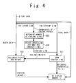
Fig. 4 is a diagram for illustrating a detailed
operation of the font drawing circuit 11 for
generating the rectangular area data 13. The font
drawing circuit 11 provides the below-mentioned
process operations for each of the lines described in
the font data 6.
The font drawing circuit 11 determines whether
each of the lines to be processed is a straight line,
or a curved line. In the case that the relevant line
is a straight line, the font drawing circuit 11
executes a line drawing calculation at Step S01. In
this line drawing calculation, the font drawing
circuit 11 calculates a set of x and y reference
coordinates x0 and y0, and inclination data
representative of an inclination of the straight line
for each rectangular area, on the basis of the
coordinates of the control points located on both ends
of the centerline of the straight line to be processed.
Furthermore, the font drawing circuit 11 executes a
width/height calculation at Step S02, which involves
calculating the width "W" and height "h" of each
rectangular area from the inclined data and width data
of the relevant straight line described in the font
data 6. The rectangular area data 13 is produced
through executing the line drawing calculation and the
width/height calculation.
The process operations executed in the line
drawing calculation and the width/height calculation
depends on the inclinations calculated in the line
drawing calculation. In the case that the straight
line to be processed is a horizontal line (namely,
line along x direction), as shown in Fig. 3C, the font
drawing circuit 11 defines a rectangular area to cover
the horizontal line, in which pixels having the same
color are arranged in rows and columns. The font
drawing circuit 11 then calculates the x and y
reference coordinates x0 and y0 and the width W of the
relevant rectangular area from the coordinates of the
control points defined on both ends of the centerline
of the straight line to be processed. Additionally,
the font drawing circuit 11 determines the height "h"
of the relevant rectangular area as being the value of
the width data of the relevant straight line described
in the font data 6. The x and y reference coordinates
x0 and y0 are defined so that the x and y reference
coordinates x0 and y0 corresponds to the median point
of the centerline of the relevant straight line.
A similar process operation is carried out in
the case that the straight line to be processed is a
vertical line (namely, a line along y direction). The
font drawing circuit 11 defines a rectangular area to
cover the vertical line, in which pixels having the
same color are arranged in rows and columns. The font
drawing circuit 11 calculates the height "h" of the
rectangular area from coordinates of control points
located on both edges of the centerline of this
vertical line, and determines the width "W" of the
rectangular area as being the value of the width data
of the vertical line described in the font data 6.
In such a case that the straight line to be
processed is to an inclined line, the font drawing
circuit 11 produces the rectangular area data 13 so
that the relevant inclined line is expressed by a
plurality of rectangular areas. It should also be
understood that these plural rectangular areas may be
overlapped with each other, as indicated in Fig. 3B.
Specifically, the font drawing circuit 11 determines
the x and y reference coordinates x0 and y0 of each
rectangular area so that the x and y reference
coordinates x0 and y0 corresponds to a point located
on the centerline of the inclined line. Further, the
font drawing circuit 11 calculates the width "W" and
height "h" of each rectangular area on the basis of
the inclination data and width data associated with
the straight line to be processed.
On the other hand, in the case that the line to
be processed is a cured line, the font drawing circuit
11 approximates the curved line by employing a
plurality of short straight lines. The font drawing
circuit 11 firstly determines a number of lines used
to approximate the curved line, which may be referred
to as the division number, on the basis of the
coordinates of the control points of the cured line at
Step S03. Furthermore, the font drawing circuit 11
divides the relevant curved line into a set of short
straight lines, the total number of which is equal to
the division number, and calculates coordinates of
both ends of the straight lines obtained by dividing
the relevant curved line as the coordinates of the
control points of the obtained straight lines at Step
S04. The font drawing circuit 11 then executes the
above-described process operations defined in the
Steps S01 and S02 for each of the obtained straight
lines so as to produce the rectangular area data 13.
The rectangular area data 13 determined for the
respective rectangular areas are sequentially
transmitted to the image memory 12. The pixel data of
the pixels located within each rectangular area are
simultaneously written into the image memory 12 in
response to the rectangular area data 13. This
procedure effectively achieves developing the bitmap
data 5 onto the image memory 12 in a high speed.
6) Intermediate Summary
As previously explained, the display device 10
of the first embodiment is adapted to concurrently
write pixel data of multiple pixels arranged in a
rectangular area onto the image memory 12, when the
relevant pixels are programmed with the same pixel
data, associated with the same color. In other words,
the display device 10 is adapted to the pixel data
representative of the same colors into a plurality of
pixel blocks 33 arranged over a plurality of rows and
columns. The display device 10 such designed
effectively enhances the access speed to the image
memory 12 during developing the bitmap data 5.
The image processing operation executed in the
stroke font processing circuit 4 in this embodiment is
applicable to the processing of an image that contains
a large number of pixels associated with the same
color, such as a draw graphic image. In this case,
shape data indicative of graphic primitives
incorporated within the relevant image is sent to an
image processor circuit, and then, this image
processing circuit defines a set of rectangular areas
for the graphic primitives so that each rectangular
area incorporates pixels associated with the same
color. The image processing circuit produces
rectangular area data that represents a position, a
color, a width, and a height of each rectangular area,
and writes the pixel data of the pixels within each
rectangular area onto the image memory at the same
time on the basis of the produced rectangular data.
The above-described image processing method achieves
high-speed generation of the desired image data
associated with the image containing a large number of
the same color pixels onto the image memory.
In an alternative embodiment, image data
indicative of the shapes of the characters, which does
not represent the colors of the characters, may be
developed onto the image memory 12 instead of the
bitmap-formatted image data (namely, bitmap data 5
constructed of RGB data). For example, binary data
may be developed onto image memory 12. In this case,
pixel data associated pixels located within a
character to be drawn are set to, for example, "1",
whereas pixel data of pixels that are not located
within the characters are set to, for instance, "0".
Second Embodiment
In a second embodiment of the present invention,
the structure and operations of the display device is
modified to reduce an amount of a process operation
loaded to the stroke font drawing circuit 11;
operations of the stroke font drawing circuit 11 are
modified as shown in Fig. 11 and Fig. 12, and the
structure of the image memory 12 is also modified as
represented in Fig. 13.
Fig. 11 illustrates the operations of the
stroke font drawing circuit 11 in the second
embodiment. The stroke font drawing circuit 11
performs the operations shown in Fig. 11 for each
relevant line incorporated within the characters to be
displayed.
For the case that the relevant line is a curved
line, the curved line is divided into a set of
straight lines at Step S11; for the case that the
relevant line is a straight line, Step S11 is skipped.
Subsequently, a centerline of a relevant
straight line is subdivided into a set of vertical
lines, horizontal line(s), and dots in an approximate
manner at Step S12. It should also be understood that
the relevant straight line to be processed at Step S12
may be the relevant line to be processed, and one of
the straight lines obtained by dividing the curved
line.
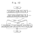
Fig 12 is a flow chart representing an
algorithm by which the centerline of the relevant
straight line is subdivided into a set of vertical
line(s), horizontal line(s), and dot(s). First,
coordinates of both ends of the centerline of the
relevant straight line are obtained at Step S12-1.
The ends of the centerline will be referred to as
points "A" and "B", hereinafter. At Step S12-2, the
stroke font drawing circuit 11 then determines a
distance "dx" between the points A and B along the x
direction, and another distance "dy" between the
points A and B along the y direction. The distances
"dx" and "dy" are represented by the following
formulas:
dx = |xA - xB | + 1,
and
dy = |yA - yB | + 1,
where (xA, yA) are coordinates of the point A (one end
of the centerline), and (xB, yB) are coordinates of the
point B (the other end of the centerline). The
coordinates xA, yA, xB, and yB are all represented by
integers indicative of the addresses of the associated
pixels. It should be understood that the distances
"dx" and "dy" are also integers, which are obtained
from the coordinates (xA, yA) and (xB, yB).
This is followed by comparing the distance "dx"
with the distance "dy" at Step S12-3 to determine
whether the centerline of the relevant straight line
is a "longitudinal" line, or a "horizontal" line.
When the distance dx is longer than the
distance dy, the centerline is divided into "dy"
pieces of horizontal lines at Step S12-4. For example,
in a case that the coordinates of points A and B,
which are the ends of a relevant centerline, are (0,
0) and (5, 1), respectively, the relevant centerline
is divided into two horizontal lines: That is, the
relevant centerline is subdivided to a first
horizontal line having the ends located on the
coordinates (0, 0) and (2, 0), and a second horizontal
line having the ends located on the coordinates (3, 1)
and (5, 1).
Lengths of the horizontal lines obtained
through dividing the relevant centerline are given as
follows:
In the case that the distance "dx" is shorter
than the distance "dy", on the other hand, the
centerline is subdivided into "dx" pieces of vertical
lines at Step S12-5. A method for subdividing this
centerline into a set of vertical lines is identical
to the method for subdividing the centerline into the
horizontal lines.
In such a case that the distance "dx" is equal
to the distance "dy", the relevant centerline is
subdivided into "dx" pieces (="dy" pieces) of dots at
Step S12-6.
In the second embodiment, rectangular areas are
defined for each of the horizontal lines, the vertical
lines, and the dots, which are produced by dividing
the centerlines; reference coordinates indicative of a
position of each rectangular area are determined for
each of the horizontal lines, the vertical lines, and
the points.
In this embodiment, two sets of reference
coordinates are given for each rectangular area; the
two sets of the reference coordinates (x0, y0) and (x1
y1
) are defined as follows. For a horizontal line and
a vertical line, the reference coordinates (x0, y0)
and (x1, y1) are determined from coordinates (xP, yP)
and (xQ, yQ) of points "P" and "Q" located on both
ends of the horizontal line and the vertical line in
accordance with the following formulas:
x0 = max (xP, xQ),
x1 = min (xP, xQ),
y0 = max (yP, yQ),
and
y1 = min (yP, yQ).
On the other hand, as to a dot, the reference
coordinates (x0, y0) and (x1, y1) are determined from
coordinates (xR, yR) of the relevant dot in accordance
with the following formulas:
x0 = x1 = xR,
and
y0 = y1 = yR.
The stroke font drawing circuit 11 produces
rectangular area data 13 for each rectangular area so
that the rectangular area data 13 incorporates two
sets of the reference coordinates (x0, y0) and (x1,y1
); the width data; and the pixel data, and supplies
the produced rectangular area data 13 to the image
memory 12. As will be explained later, the reference
coordinates (x0, y0), (x1, y1), and the width data are
used to calculate the maximum value xMAX and minimum
value xMIN of x addresses of each rectangular area, and
also to calculate the maximum value yMAX and minimum
value yMIN of y addresses of each rectangular area; the
reference coordinates and the width data are
representative of the position, the width, and the
height of the relevant rectangular area.
In response to the rectangular area data 13,
incorporating the reference coordinates (x0, y0), (x1,y1
), the width data, and the pixel data), the stroke
font drawing circuit 11 writes the pixel data of the
associated pixels onto the image memory 12 at the same
time for each rectangular area.
Specifically, the y address control circuit 21
calculates the maximum value yMAX and minimum value yMIN
of the y addresses of each rectangular area from the
reference coordinates (x0, y0), (x1, y1), and the
width data. Correspondingly, the x address control
circuit 24 calculates the maximum value xMAX and
minimum value xMIN of the x addresses of each
rectangular area from the reference coordinates (x0,
y0), (x1, y1), and the width data.
Various methods may be used for calculating the
maximum value yMAX, the minimum value yMIN, the maximum
value xMAX, and the minimum value xMIN.
In one embodiment, different formulas are used
for calculating the maximum value yMAX, the minimum
value yMIN, the maximum value xMAX, and the minimum
value xMIN depending on whether the width "ϕ" is an odd
number or an even number, the width "ϕ" being
described as the width data within the rectangular
area data 13. For a width "ϕ" being an odd number,
the maximum value xMAX, the minimum value xMIN, the
maximum value yMAX, and the minimum value yMIN may be
calculated by the following formulas:
xMAX = x0 + ϕ/2,
xMIN = x1 - ϕ/2,
yMAX = y0 + ϕ/2,
and
yMIN = y1 - ϕ/2.
For a width "ϕ" being an even number, on the
other hand, the maximum value xMAX, the minimum value
xMIN, the maximum value yMAX, and the minimum value yMIN
may be calculated by the following formulas:
xMAX = x0 + ϕ/2,
xMIN = x1 - ϕ/2 - 1,
yMAX = y0 + ϕ/2,
and
yMIN = y1 - ϕ/2 - 1 .
Alternatively, for a width "ϕ" being an even
number, the maximum value xMAX, the minimum value xMIN,
the maximum value yMAX, and the minimum value yMIN may
be calculated by the following formulas:
xMAX = x0 + ϕ/2 - 1,
xMIN = x1 - ϕ/2,
yMAX = y0 + ϕ/2 - 1,
and
yMIN = y1 - ϕ/2.
In an alternative embodiment, independently of
whether the width "ϕ" is odd or even, the maximum
value xMAX, the minimum value xMIN, the maximum value
yMAX, and the minimum value yMIN may be calculated by
the following formulas:
xMAX = x0 + ϕ,
xMIN = x0,
yMAX = y0 + ϕ,
and
yMIN = y0.
Instead, the maximum value xMAX, the minimum
value xMIN, the maximum value yMAX, the minimum value
yMIN may be calculated by the following formulas:
xMAX = x0,
xMIN = X0 - ϕ,
yMAX = Y0,
and
yMIN = Y0 - ϕ.
The Y area selecting circuit 22 then selects
the y address signals 280 to 28M-1 in response to the
maximum value yMAX and minimum value yMIN of the y
addresses of the relevant rectangular area. One or
more of the y address signals 280 to 28M-1 are selected,
which are associated with y addresses ranging between
the maximum value yMAX and minimum value yMIN.
In response to the y address signals 280 to
28M-1, the word line decoder 23 activates the associated
word lines 31. When a plurality of y addresses are
selected, two or more of the word lines 31 are
activated at the same time. The memory cells 34
connected to the activated word lines 31 are
electrically connected to the bit lines 32.
Correspondingly, the X area selecting circuit
25 selects the x address signals 290 to 29N-1 in
response to the maximum value xMAX and minimum value
xMIN of the x addresses of the relevant rectangular
area. One or more of the x address signals 290 to
29N-1 are selected, which are associated with x addresses
ranging between the maximum value xMAX and minimum
value xMIN.
In response to the x address signals 290 to
29N-1, the bit line decoder 26 connects the bit lines 32
associated with the selected x addresses to the signal
lines transferring the pixel data to the image memory
12. As a consequence, the pixel data are written into
the selected pixel blocks 33. In other words, the
data bits of the pixel data are written into the
associated memory cells 34 within the selected pixel
blocks 33.
An advantageous feature of the display device
in the second embodiment is simplicity of the
calculation operations performed by the stroke font
drawing circuit 11; the amount of processing performed
by the stroke font drawing circuit 11 is effectively
reduced compared to the first embodiment. This is
effective for achieving high-speed "drawing of
characters" onto the image memory 12.
Third Embodiment
Fig. 14 is a block diagram schematically
showing an exemplary of a display device 20 according
to a third embodiment of the present invention. The
display device 20 of the third embodiment incorporates
a control driver adapted to generate pixel data in
response to externally inputted stroke font data, and
to drive an LCD panel on the basis on the generated
pixel data. The generated pixel data are stored in a
memory constructed in the same manner as the image
memory 12 used in the first and second embodiments,
which are designed to write pixel data associated with
a plurality of pixels arranged in multiple rows and
columns at the same time. A detailed description is
made of the display device 20 in the third embodiment.
In the third embodiment, the display device 20
is equipped with a CPU 61, a controller driver 62, and
an LCD panel 63 incorporating pixels arranged in a
matrix. The CPU 61 provides the controller driver 62
with display data associated to an image to be
displayed on the LCD panel 63. The CPU 61
additionally provides a control signal 66, and color
palette data 67 for the controller driver 62. The
controller driver 62 is responsive to the display data,
the control signal 66, and the color palette 67 for
driving the LCD panel 63, and thereby displaying a
desired image thereon.
The display data, which are supplied from the
CPU 61 to the controller driver 62, includes two sorts
of data: bitmap data 64 associated with a background
image, and font data 65 associated with characters to
be superimposed on the background image.
The bitmap data 64 is composed of pixel data
represented in an RGB format, indicative of R, G, B,
grayscale levels of each pixel.
The font data 65 is represented in a stroke
font format, describing characters to be displayed on
the LCD panel 63. The use of the stroke font format
for transmitting characters to be displayed is
effective for reducing the size of the display data.
Generally speaking, the size of font data described in
a stroke font format is approximately one-fourth of
that described in a bitmap format.
In this embodiment, the font data 65 designates
the color of each character using of an n-bit color
reference number in place of RGB data. It should be
noted that the number of usable colors for
representing a certain character is equal to 2n, when
an n-bit color reference number is used for
designating the color thereof. The n-bit color
reference number are defined so that the number of the
usable colors for representing characters is smaller
than that of the usable colors for displaying images
on the LCD panel 63. In this third embodiment, each
color reference number ranges from 0 to 3, represented
by two data bits. The use of color reference numbers
provides an advantage that the controller driver 62
requires a reduced storage capacity for storing the
display data.
The color palette data 67 describes an
association of the color reference numbers described
in the font data 65 with RGB data associated with
usable colors, (namely, sets of data indicative of R,
G, B grayscale levels). Fig. 15 is an explanatory
diagram conceptually illustrating contents of the
above-described color palette data 67. A color
reference number of "1", for example, is associated
with "blue" (that is, associated with RGB data
corresponding to "blue"); another color reference
number of "2" is associated with "red" (that is,
associated with RGB data corresponding to "red"); and
still another color reference number of "3" is
associated with "yellow" (that is, associated with RGB
data corresponding to "yellow").
Referring back to Fig. 14, the controller
driver 62 is equipped with a control circuit 71, an
image display memory 72, a stroke font drawing circuit
73, a font process memory 74, a font display memory 75,
a filter 76, a color palette circuit 77, and a drive
circuit 78. The control circuit 71 is responsive to
the control signal 66 received from the CPU 62 for
controlling the circuits incorporated within the
controller driver 62. Firstly, the control circuit 71
forwards data received from the CPU 61 to the
appropriate destination. Specifically, the control
circuit 71 forwards the bitmap data 64 to the image
display memory 72, while forwarding the font data 65
to the stroke font drawing circuit 73. Furthermore,
the control circuit 71 forwards the color palette data
67 to the color palette circuit 77. Finally, the
control unit 71 provides a timing control signal 79
for the drive circuit 78 so as to control operation
timing of the drive circuit 78, and provides a
calculation control signal 80 for the filter 76 in
order to indicate a calculation which should be
carried out by the filter 76.
The image display memory 72 receives the bitmap
data 64, associated with the background image, from
the control circuit 71, and stores thereinto the
received bitmap data 64.
The stroke font drawing circuit 73 is designed
similarly to the stroke font drawing circuit 11
according to the first embodiment (or the second
embodiment). The stroke font drawing circuit 73 is
designed to acknowledge the shape of each relevant
character from the font data 65, and defines a set of
rectangular areas so that each rectangular area
incorporates pixels associated with the same color.
As previously explained, two or more of the
rectangular areas may be overlapped with each other.
Furthermore, the stroke font drawing circuit 73
produces rectangular area data 81 for each rectangular
area. The rectangular area data 81 includes contents
similar to those of the rectangular area data 13 of
the first embodiment (or the second embodiment).
Specifically, each rectangular area data 81 is
representative of x and y reference coordinates x0 and
y0 of the associated rectangular area, describing the
width "W" of the associated rectangular area along an
x axis direction and the height "h" thereof along a y
axis direction, and the color reference number for
designating the color of the associated rectangular
area. It should be noted that the color of each
rectangular area is designated within the rectangular
area data 81 using a color reference number instead of
RGB data.
The font process memory 74, designed to
similarly to the image memory 12 of the first
embodiment (or the second embodiment), stores therein
color reference number data 82 composed of pixel data
of the characters to be displayed, which represents
the colors of the characters using color reference
numbers. The font process memory 74 generates the
color reference number data 82 on the basis of the
rectangular area data 81 received from the stroke font
drawing circuit 73. Specifically, the font process
memory 74 sequentially receives the rectangular area
data 81 from the stroke font drawing circuit 73, and
the font process memory 74 writes the color reference
number data described in the transmitted rectangular
area data 81 into pixel blocks associated with the
pixels incorporated within the associated rectangular
area at the same time. This achieves the development
of the color reference number data 82 onto the font
process memory 74 to thereby complete the "drawing of
the characters".
The font display memory 75 receives the color
reference number data 82 from the font process memory
74, and then stores thereinto the received color
reference number data 82. The color reference number
data 82 stored in the font display memory 75 is used
to display the desired characters on the LCD panel 63.
The filter 76 is designed to synthesize the
characters to be displayed with the background image;
the filter 76 generates synthesized image bitmap data
83 through executing image calculation, such as on-screen
calculation and α blend, for synthesizing the
characters with the background image on the LCD panel
63. The filter 76 is responsive to the control signal
80 transmitted from the control circuit 71 for
executing the image calculation. When the control
signal 80 indicates the filter 76 to display the
background image on the LCD panel 63 as it is, the
filter 76 simply forwards the bitmap data 64,
associated with the background image, from the image
display memory 72 to the drive circuit 78. When the
control circuit 71 requests the filter 76 to execute
image calculation for synthesizing the characters with
the background image, on the other hand, the filter 76
receives the bitmap data 64 from the image display
memory 72 in units of rows of the pixels, and also
receives the color reference data 82 from the font
display memory 75 in units of rows of the pixels.
Referring to the color palette data 67 stored in the
color palette circuit 77, the filter 76 converts the
color reference number data 82, which represent the
colors of the pixels with color reference numbers,
into the corresponding RGB data. The filter 76
performs image calculation on the basis of the RGB
data produced by the conversion and the RGB data of
the bitmap data 64, to thereby generate the
synthesized image bitmap data 83.
The drive circuit 78 receives selected one of
the bitmap data 64 of the background image and the
synthesized image bitmap data 83 from the filter 76,
and drives data lines (not shown) of the LCD panel 63
in response to the received bitmap data 64, or 83.
Timing for driving the data lines of the LCD panel 63
is controlled in response to the timing control signal
79 received from the control apparatus 71.
It should be noted that the color reference
number data 82 produced in the font process memory 74
is not directly used to display the character on the
LCD panel 63. This addresses avoiding incomplete
characters being displayed on the LCD panel 63. As
previously explained, the generation of the color
reference number data 82 onto the font process memory
74 involves sequentially interpreting the commands
described in the font data 6; it is not until the
process operations of the rectangular area data 81 of
the rectangular areas are completed for all the
relevant characters, that the color reference number
data 82 is accomplished onto the font process memory
74. The time duration required for accomplishing the
color reference number data 82 cannot be neglected, as
compared with the refresh cycle time of the LCD panel
63. As a consequence, if the color reference number
data 82 produced in the font process memory 74 is
directly used to be displayed on the LCD panel 63,
incomplete characters may be displayed on the LCD
panel 63. The architecture in which the font display
memory 75 is provided separately from the font process
memory 74 effectively avoids incomplete characters
being displayed on the LCD panel 63. The controller
driver 62 is designed to transfer the color reference
number data 82 from the font process memory 74 to the
font display memory 75 after completing the color
reference number data 82 onto the font process memory
74. The filter 76 and the drive circuit 77 use the
completed color reference number data 82 received from
the font display memory 75 so as to perform the on-screen
display. This effectively avoids incomplete
characters being displayed on the LCD panel 63.
Fig. 16 is a block diagram for representing
operations of the controller driver 62 for
synthesizing desired characters with a background
image.
Upon receiving the bitmap data 64 associated
with the background image and the font data 65
associated with characters from the CPU 61, the
control circuit 71 forwards the bitmap data 64 to the
image display memory 72, and the font data 65 to the
font drawing circuit 73. The bitmap data 64 is
written onto the image display memory 72. In the case
that the color palette data 67 is transmitted from the
CPU 61, the control circuit 71 forwards the color
palette data 67 to the color palette circuit 77.
The font drawing circuit 73 sequentially
interprets commands described in the font data 65 to
acknowledge the shape of each character to be
displayed. The font drawing circuit 73 then defines
rectangular areas for each relevant character, and
develops the rectangular area data 81 associated with
the rectangular areas. This is followed by
sequentially forwarding the rectangular area data 81
from the font drawing circuit 73 to the font process
memory 74 so as to perform "drawing of the characters"
onto the font process memory 74. The pixel data of
the complete set of the pixels incorporated within
each rectangular area are written into the font
process memory 74 at the same time. This effectively
enhances the operation speed for completing "drawing
of characters". As a result of a completion of
"drawing of the characters", color reference number
data 82 is produced onto the font process memory 74.
After completing the color reference number data
82 onto the font process memory 74, the color
reference number data 82 is transferred to the font
display memory 75. The transfer of the color
reference number data 82 to the font display memory 75
is carried out within a short time duration, as
compared with the refresh cycle of the LCD panel 63.
The filter 76 receives the bitmap data 64
associated with the background image from the image
display memory 72, and also receives the color
reference number data 82 from the font display memory
75. The filter 76 then produces the synthesized image
bitmap data 83 in response to the bitmap data 64 and
the color reference number data 82. The filter 76
converts the color reference numbers of the color
reference number data 82 into RGB data, and produces
the synthesized image bitmap data 83 on the basis of
the RGB data obtained by the data conversion and the
RGB data of the bitmap data 64. The drive circuit 77
drives the LCD panel 63 in response to the synthesized
image bitmap data 83 received from the filter 76, so
that the image in which the character has been
superimposed on the background image is displayed on
the LCD panel 63.
In summary, similarly to the first embodiment,
the display device 20 of the third embodiment is
designed to write pixel data of multiple pixels
arranged in a certain rectangular area onto the font
process memory 74 at the same time, when the colors of
the relevant pixels are identical to each other,
written. This achieves high-speed generation of the
color reference data 82 onto the font process memory
74.
In addition, in the display device 20 of the
third embodiment, the use of the color reference
number data 82, which represents the color of each
pixel by an color reference number, effectively
reduces the storage capacities of both the font
process memory 74 and the font display memory 75.
Finally, the controller driver architecture in
this third embodiment effectively reduces the size of
the display data transferred to the controller driver
62 through transmitting the font data 65 in a stroke
font format. This effectively reduces the power
consumption of the controller driver 62.
Although the invention has been described in
its preferred form with a certain degree of
particularity, it is understood that the present
disclosure of the preferred form has been changed in
the details of construction and the combination and
arrangement of parts may be resorted to without
departing from the scope of the invention as
hereinafter claimed.